Design Procedure for sequential circuits The word description


 ● d=f")


- Slides: 7
Design Procedure for sequential circuits: ● The word description of the circuit behavior to get a state diagram. ● State reduction if necessary. ● Assign binary values to the states. ● Obtain the binary-coded state table. ● Choose the type of flip-flops. ● Derive the simplified flip-flop input equations and output equations. ● Draw the logic diagram. Example 3: Design the sequential circuit that has the specification given in the state diagram shown, for the input sequence 01010110100 starting from the initial state a. 46
State diagram 2 - State table 47
3 Reducing the state table: ● e=g (remove g and keep e) ● d=f (remove f and keep d) 48
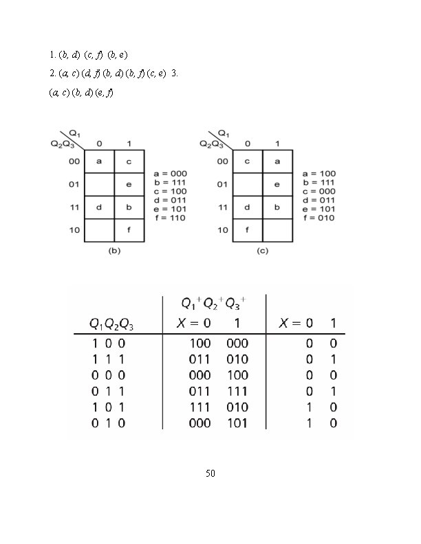
"State diagram after reduction" 4 - State Assignment: Guidelines for State Assignment: Example 4: Selecting an Assignment. 49
5. Choose the D type of flip-flops. 6. Derive the simplified flip-flop input equations and output equations. Homework: 7. Finally draw the logic diagram. 51
Example 5: Consider the state table given below: Present Next state X=0 X=1 1 2 3 4 5 6 7 2 4 2 6 2 3 3 5 3 7 Output (Z) X=0 X=1 0 0 0 0 1 The state of adjacent states specified by guidelines 1&2 are: 1. (1, 3, 5, 7) (4, 6) (1, 2, 4, 6) (5, 7) 2. (2, 3) (3, 4) (2, 5) (3, 6) (2, 7) 52