Design of Subm W RF CMOS LowNoise Amplifiers
Design of Sub-m. W RF CMOS Low-Noise Amplifiers Derek Ho Dept. of Electrical and Computer Engineering University of British Columbia March 30, 2007
Outline Motivation and Objectives n Device Characteristics n Design Methodology n 90 nm 2. 4 GHz LNA Design and Results n Conclusion and Future Work n 2
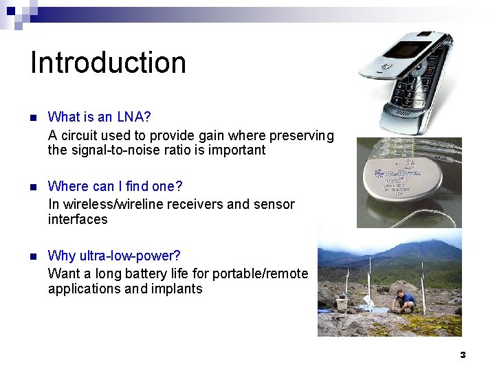
Introduction n What is an LNA? A circuit used to provide gain where preserving the signal-to-noise ratio is important n Where can I find one? In wireless/wireline receivers and sensor interfaces n Why ultra-low-power? Want a long battery life for portable/remote applications and implants 3
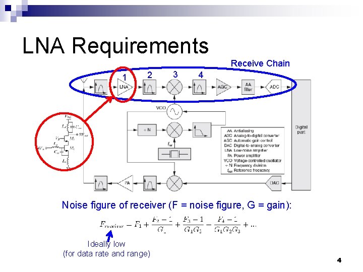
LNA Requirements Receive Chain 1 2 3 4 Noise figure of receiver (F = noise figure, G = gain): Ideally low (for data rate and range) 4
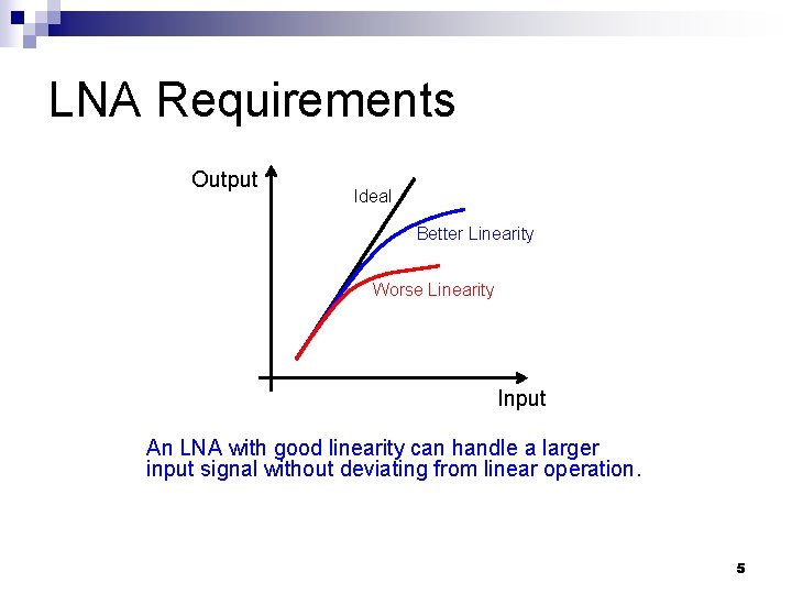
LNA Requirements Output Ideal Better Linearity Worse Linearity Input An LNA with good linearity can handle a larger input signal without deviating from linear operation. 5
LNA Design Challenges 6
Research Objectives Devise a simple methodology that leads to power-efficient LNA designs - Form a graphical toolkit to help reduce design time and improve design quality - Explore LNA power-performance tradeoffs - Find a low-voltage low-power circuit topology - Demonstrate a high performance design in a deep submicron technology 7
Outline Motivation and Objectives n Device Characteristics n Design Methodology n 90 nm 2. 4 GHz LNA Design and Results n Conclusion and Future Work n 8
![Gain and Transconductance Advantage of graphical approach: Quicker, more accurate VGS [V] n n Gain and Transconductance Advantage of graphical approach: Quicker, more accurate VGS [V] n n](http://slidetodoc.com/presentation_image_h2/8e74d252bbf585a01f2384023d399e4f/image-9.jpg)
Gain and Transconductance Advantage of graphical approach: Quicker, more accurate VGS [V] n n n strong inversion subthreshold gm [m. S] (40/0. 2) moderate inversion “gain vs. bias” (20/0. 1), (40/0. 1) strong inversion moderate inversion subthreshold f. T [GHz] “gain / frequency response vs. bias” VGS [V] Both f. T and gm are strong functions of VGS f. T a strong function of L, but largely independent of W MOSFET has poor subthreshold performance 9
![strong inversion moderate inversion subthreshold gm/ID [1/V] Transconductance Efficiency gm/ID VGS [V] n n strong inversion moderate inversion subthreshold gm/ID [1/V] Transconductance Efficiency gm/ID VGS [V] n n](http://slidetodoc.com/presentation_image_h2/8e74d252bbf585a01f2384023d399e4f/image-10.jpg)
strong inversion moderate inversion subthreshold gm/ID [1/V] Transconductance Efficiency gm/ID VGS [V] n n First proposed in 1996 for op-amp (low-frequency) design [1] Represents “gain achieved” per unit “power consumed” Decreases towards strong inversion Insensitive to W and L can first design VGS (bias) then design W (size) 10
![moderate inversion Linearity subthreshold strong inversion VGS [V] VIP 3 of a 40 nm moderate inversion Linearity subthreshold strong inversion VGS [V] VIP 3 of a 40 nm](http://slidetodoc.com/presentation_image_h2/8e74d252bbf585a01f2384023d399e4f/image-11.jpg)
moderate inversion Linearity subthreshold strong inversion VGS [V] VIP 3 of a 40 nm n. FET vs. VGS (VTH = 0. 23 V) [22] n VIP 3 (measure of linearity, the greater the better) is the highest at moderate inversion (around 0. 25 V for the 45 nm FET). 11
Outline Motivation and Objectives n Device Characteristics n Design Methodology n 90 nm 2. 4 GHz LNA Design and Results n Conclusion and Future Work n 12
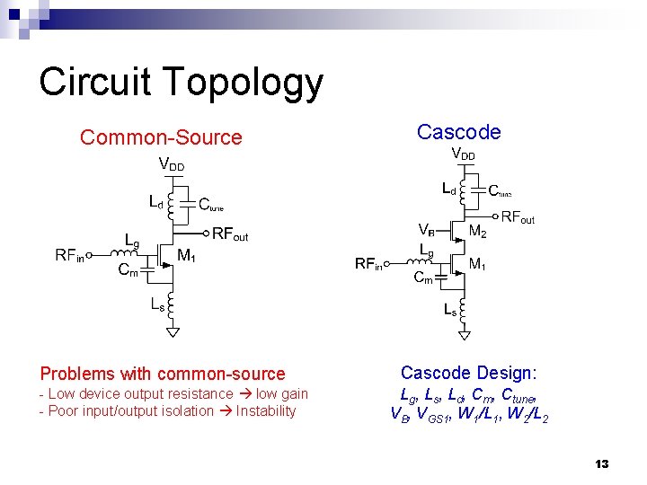
Circuit Topology Common-Source Problems with common-source - Low device output resistance low gain - Poor input/output isolation Instability Cascode Design: Lg, Ls, Ld, Cm, Ctune, VB, VGS 1, W 1/L 1, W 2/L 2 13
![NFLNA [d. B] Transistor Sizing for Noise Cascode Common-Source W [μm] n n n NFLNA [d. B] Transistor Sizing for Noise Cascode Common-Source W [μm] n n n](http://slidetodoc.com/presentation_image_h2/8e74d252bbf585a01f2384023d399e4f/image-14.jpg)
NFLNA [d. B] Transistor Sizing for Noise Cascode Common-Source W [μm] n n n NF of LNA improves with larger W However, power proportional to W Noise-power tradeoff 14
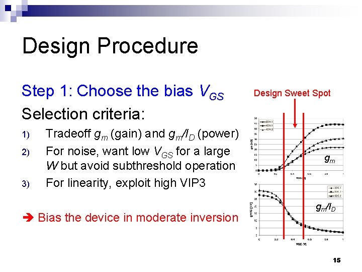
Design Procedure Step 1: Choose the bias VGS Selection criteria: 1) 2) 3) Tradeoff gm (gain) and gm/ID (power) For noise, want low VGS for a large W but avoid subthreshold operation For linearity, exploit high VIP 3 Bias the device in moderate inversion Design Sweet Spot gm gm/ID 15
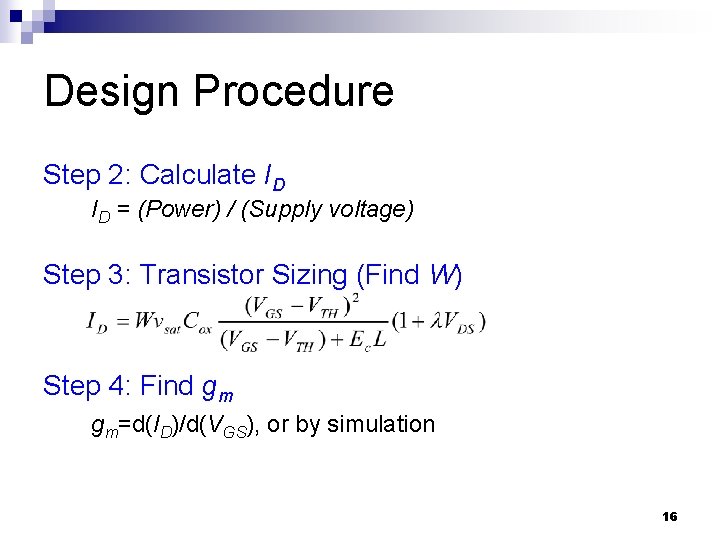
Design Procedure Step 2: Calculate ID ID = (Power) / (Supply voltage) Step 3: Transistor Sizing (Find W) Step 4: Find gm gm=d(ID)/d(VGS), or by simulation 16
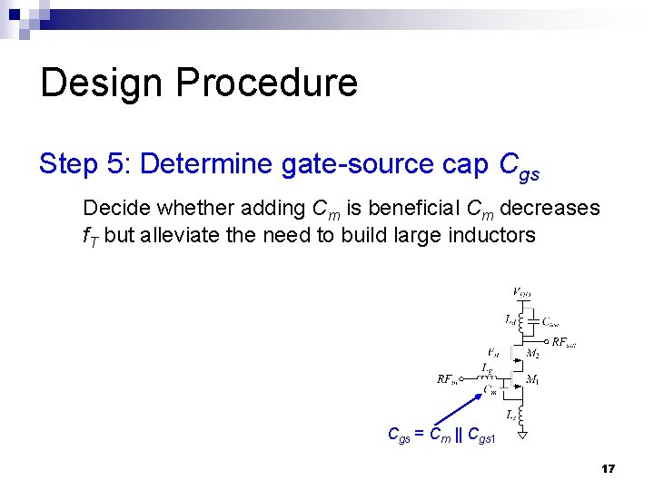
Design Procedure Step 5: Determine gate-source cap Cgs Decide whether adding Cm is beneficial Cm decreases f. T but alleviate the need to build large inductors Cgs = Cm || Cgs 1 17
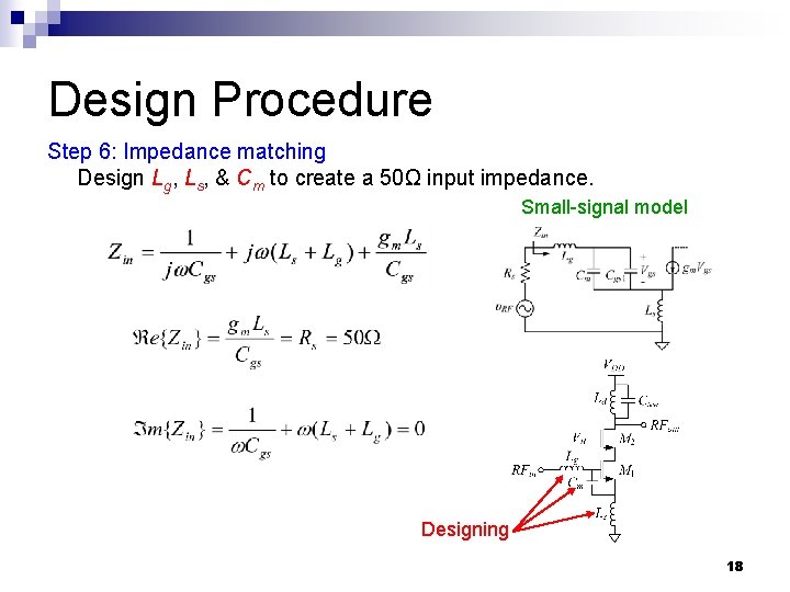
Design Procedure Step 6: Impedance matching Design Lg, Ls, & Cm to create a 50Ω input impedance. Small-signal model Designing 18
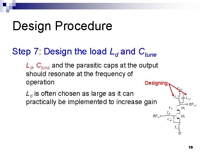
Design Procedure Step 7: Design the load Ld and Ctune Ld, Ctune and the parasitic caps at the output should resonate at the frequency of operation Designing Ld is often chosen as large as it can practically be implemented to increase gain 19
Outline Motivation and Objectives n Device Characteristics n Design Methodology n 90 nm 2. 4 GHz LNA Design and Results n Conclusion and Future Work n 20
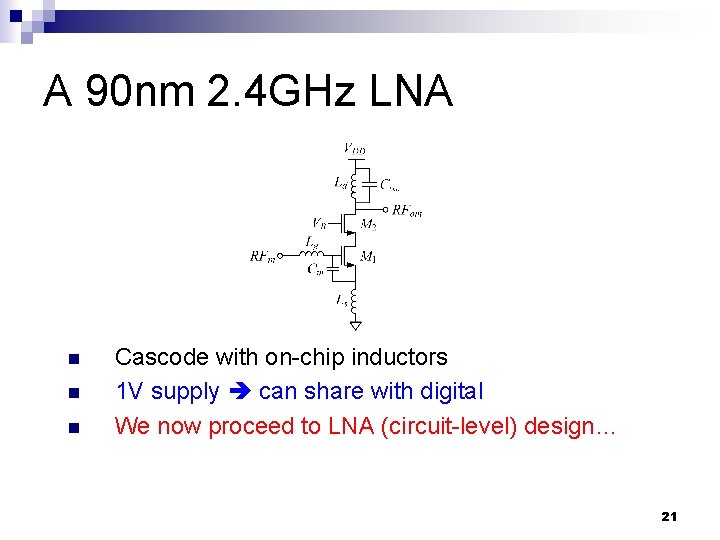
A 90 nm 2. 4 GHz LNA n n n Cascode with on-chip inductors 1 V supply can share with digital We now proceed to LNA (circuit-level) design… 21
![Gain “gain vs. size” Power VGS [V] Gain insensitive to VGS Av [d. B] Gain “gain vs. size” Power VGS [V] Gain insensitive to VGS Av [d. B]](http://slidetodoc.com/presentation_image_h2/8e74d252bbf585a01f2384023d399e4f/image-22.jpg)
Gain “gain vs. size” Power VGS [V] Gain insensitive to VGS Av [d. B] “gain vs. bias” Power W [μm] Gain does not scale well with W 22
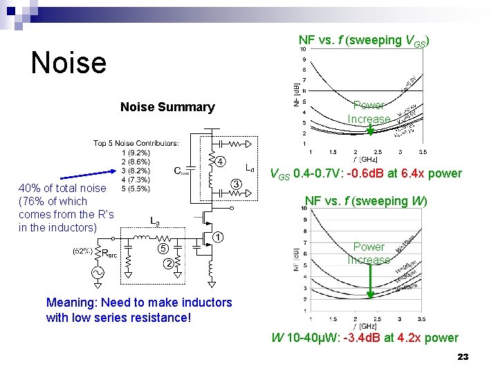
NF vs. f (sweeping VGS) Noise Summary 40% of total noise (76% of which comes from the R’s in the inductors) Power Increase VGS 0. 4 -0. 7 V: -0. 6 d. B at 6. 4 x power NF vs. f (sweeping W) Power Increase Meaning: Need to make inductors with low series resistance! W 10 -40μW: -3. 4 d. B at 4. 2 x power 23
![Linearity “LNA linearity vs. bias” IIP 3 [d. Bm] Power VGS [V] 40 nm Linearity “LNA linearity vs. bias” IIP 3 [d. Bm] Power VGS [V] 40 nm](http://slidetodoc.com/presentation_image_h2/8e74d252bbf585a01f2384023d399e4f/image-24.jpg)
Linearity “LNA linearity vs. bias” IIP 3 [d. Bm] Power VGS [V] 40 nm Linkage between LNA performance and device characteristic 24
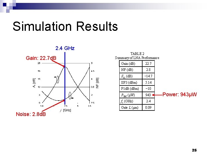
Simulation Results 2. 4 GHz Gain: 22. 7 d. B TABLE 2 Summary of LNA Performance Gain (d. B) 22. 7 NF (d. B) 2. 8 S 11 (d. B) − 14. 7 IIP 3 (d. Bm) 5. 14 P 1 d. B (d. Bm) − 10 PDC (μW) 943 fc (GHz) 2. 4 Gate L (μm) 0. 09 Power: 943μW Noise: 2. 8 d. B 25
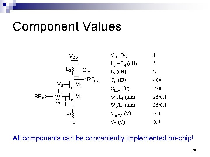
Component Values VDD (V) 1 Lg = Ld (n. H) 5 Ls (n. H) 2 Cm (f. F) 480 Ctune (f. F) 720 W 1/L 1 (μm) 25/0. 1 W 2/L 2 (μm) 25/0. 1 Vin, DC (V) 0. 4 VB (V) 0. 9 All components can be conveniently implemented on-chip! 26
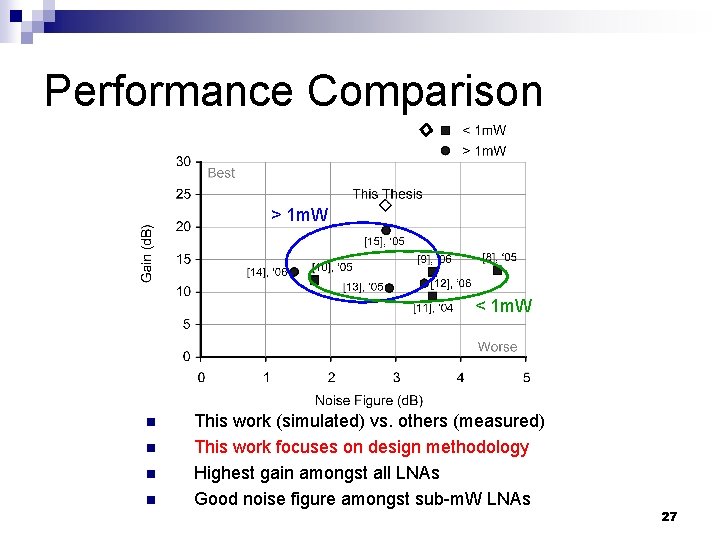
Performance Comparison > 1 m. W < 1 m. W n n This work (simulated) vs. others (measured) This work focuses on design methodology Highest gain amongst all LNAs Good noise figure amongst sub-m. W LNAs 27
Outline Motivation and Objectives n Device Characteristics n Design Methodology n 90 nm 2. 4 GHz LNA Design and Results n Conclusion and Future Work n 28
Conclusion n A design methodology was devised for sub-m. W RF CMOS LNAs having the following benefits: 1) simple to apply 2) can serve as a starting point for local optimization 3) based on the fundamental device properties The gm/ID approached previously used for low-frequency op-amp design was adopted for radio-frequency design A 2. 4 GHz 943μW LNA was designed with only manual design optimization 29
Future Work Enhancements to the proposed methodology: n Incorporate a quantitative noise analysis into the gm/ID design framework n Account for process variation and DFM concepts n Silicon verification Interesting/high-impact research areas: n Noise optimization technique for the ultra-low-power design space n Further exploitation of high FET linearity in moderate inversion 30
Related Publications 1. 2. D. Ho and S. Mirabbasi, “Design considerations for Sub-m. W CMOS RF low-noise amplifiers, ” to appear in IEEE Canadian Conference on Electrical and Computer Engineering, 2007. D. Ho and S. Mirabbasi, “Low-voltage low-power low-noise amplifier for wireless sensor networks, ” IEEE Canadian Conference on Electrical and Computer Engineering, 2006. 31
![References [1] [2] [3] [22] [28] [29] [30] [31] [32] [33] F. Silveira, D. References [1] [2] [3] [22] [28] [29] [30] [31] [32] [33] F. Silveira, D.](http://slidetodoc.com/presentation_image_h2/8e74d252bbf585a01f2384023d399e4f/image-32.jpg)
References [1] [2] [3] [22] [28] [29] [30] [31] [32] [33] F. Silveira, D. Flandre, and P. G. A. Jespers, “A gm/ID based methodology for the design of CMOS analog circuits and its application to the synthesis of a silicon-on-insulator micropower OTA, ” IEEE J. Solid-State Circuits, vol. 31, no. 9, Sep. 1996. T. -K. Nguyen, S. -K. Han, and S. -G. Lee, “Ultra-low-power 2. 4 GHz image-rejection low-noise amplifier, ” Electronics Letters, vol. 41, no. 15, July 2005. D. B. G. Perumana, S. Chakraborty, C. -H. Lee, and J. Laskar, “A fully monolithic 260 -μW, 1 -GHz subthreshold low noise amplifier, ” IEEE Microwave and Wireless Components Letters, vol. 15, no. 6, Jun 2005. Ming Cai, “Design studies of nanometer-gate low-noise amplifier near the limits of CMOS scaling, ” Doctor of Philosophy Thesis, University of California, San Diego, CA, 2006. S. B. T. Wang, A. M. Niknejad, and R. W. Brodersen, “Design of a sub-m. W 960 -MHz UWB CMOS LNA, ” IEEE J. Solid-State Circuits, vol. 41, no. 11, Nov. 2006. D. Linten, L. Aspemyr, W. Jeamsaksiri, J. Ramos, A. Mercha, S. Jenei, S. Thijs, R. Garcia, H. Jacobsson, P. Wambacq, S. Donnay, and S. Decoutere, “Low-power 5 GHz LNA and VCO in 90 nm RF CMOS, ” IEEE Sym. on VLSI Circuits, June 2004. S. Asgaran, M. J. Deen, and C. -H. Chen, “A 4 -m. W monolithic CMOS LNA at 5. 7 GHz with the gate resistance used for input matching, ” IEEE Microwave and Wireless Components Letters, vol. 16, no. 4, Apr. 2006. L. -H. Lu, H. -H. Hsieh, and Y. -S. Wang, “A compact 2. 4/5. 2 -GHz CMOS dual-band low-noise amplifier, ” IEEE Microwave and Wireless Components Letters, vol. 15, no. 10, Oct. 2005. T. -S. Kim and B. -S. Kim, “Post-linearization of cascode CMOS low noise amplifier using folded PMOS IMD sinker, ” IEEE Microwave and Wireless Component Letters, vol. 16, no. 4, Apr. 2006. M. Shouxian, M. Jian-Guo, Y. K. Seng, and D. M. Anh, “A modified architecture used for input matching in CMOS low-noise amplifiers, ” IEEE Trans. on Circuits and Systems II, vol. 52, no. 11, Nov. 2005. 32

Thank you! 33

Appendices 34
![I-V Characteristics (90 nm n. FET) VGS = 0. 7 V ID [m. A] I-V Characteristics (90 nm n. FET) VGS = 0. 7 V ID [m. A]](http://slidetodoc.com/presentation_image_h2/8e74d252bbf585a01f2384023d399e4f/image-35.jpg)
I-V Characteristics (90 nm n. FET) VGS = 0. 7 V ID [m. A] 1 m. W VGS = 0. 6 V 0. 5 m. W VGS = 0. 5 V 0. 1 m. W VGS = 0. 4 V VGS = 0. 3 V VDS [V] n n ID scales with W, ID does not scale with 1/L Bias selection with constant power contours 35
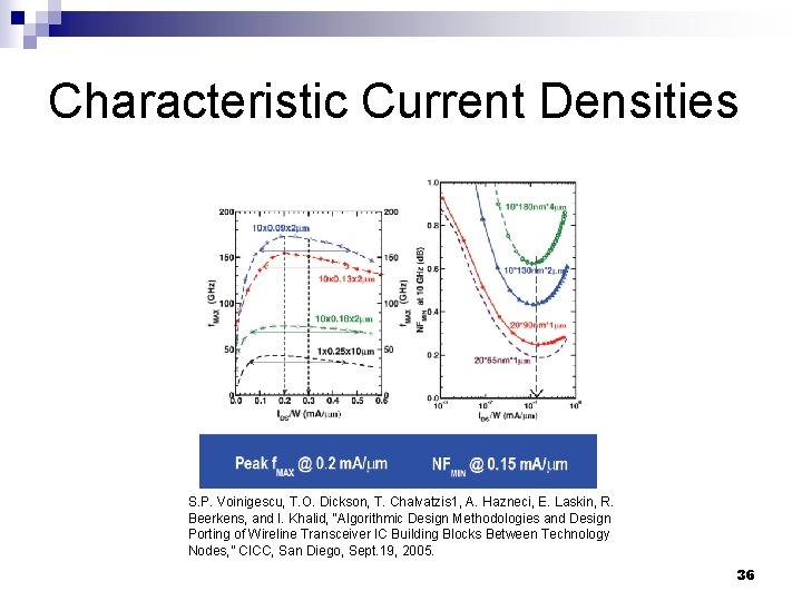
Characteristic Current Densities S. P. Voinigescu, T. O. Dickson, T. Chalvatzis 1, A. Hazneci, E. Laskin, R. Beerkens, and I. Khalid, “Algorithmic Design Methodologies and Design Porting of Wireline Transceiver IC Building Blocks Between Technology Nodes, ” CICC, San Diego, Sept. 19, 2005. 36
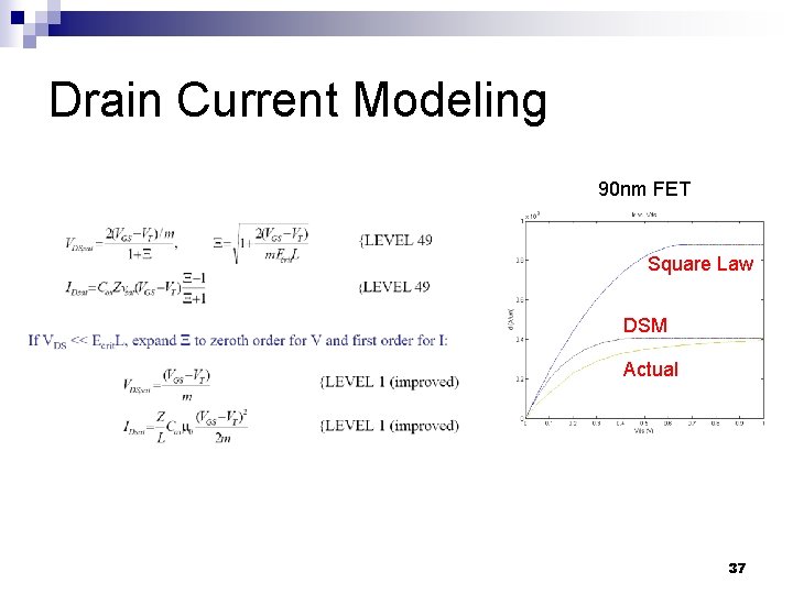
Drain Current Modeling 90 nm FET Square Law DSM Actual 37
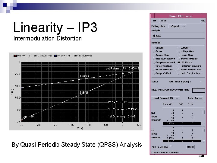
Linearity – IP 3 Intermodulation Distortion By Quasi Periodic Steady State (QPSS) Analysis 38
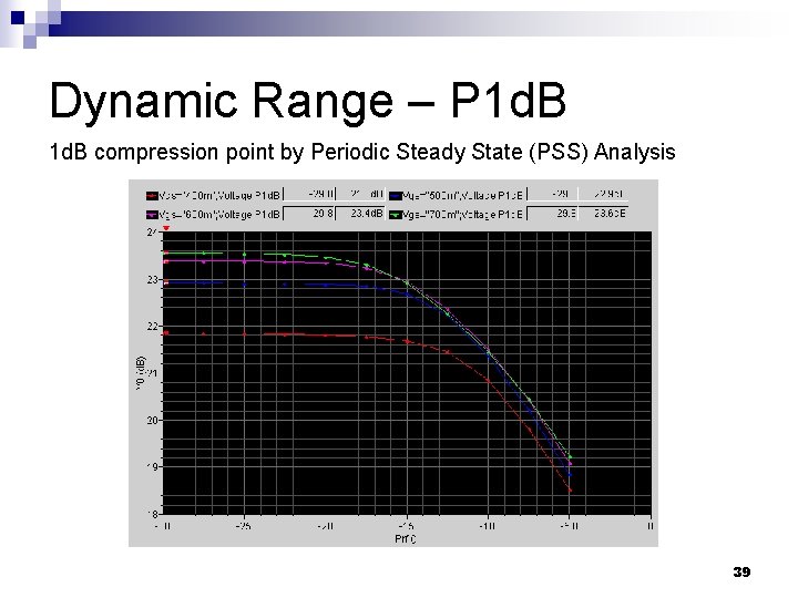
Dynamic Range – P 1 d. B compression point by Periodic Steady State (PSS) Analysis 39
- Slides: 39