DESIGN OF REGULAR CLASSICAL AND QUANTUM CIRCUITS CLASSIC

![Example of Positive Davio Lattice from [Perkowski 97 d]. Positive Davio Expansion is applied Example of Positive Davio Lattice from [Perkowski 97 d]. Positive Davio Expansion is applied](https://slidetodoc.com/presentation_image_h2/e21803d3fa08f66dd6a9ffe55e10974a/image-55.jpg)
- Slides: 80

DESIGN OF REGULAR CLASSICAL AND QUANTUM CIRCUITS

CLASSIC AL 2

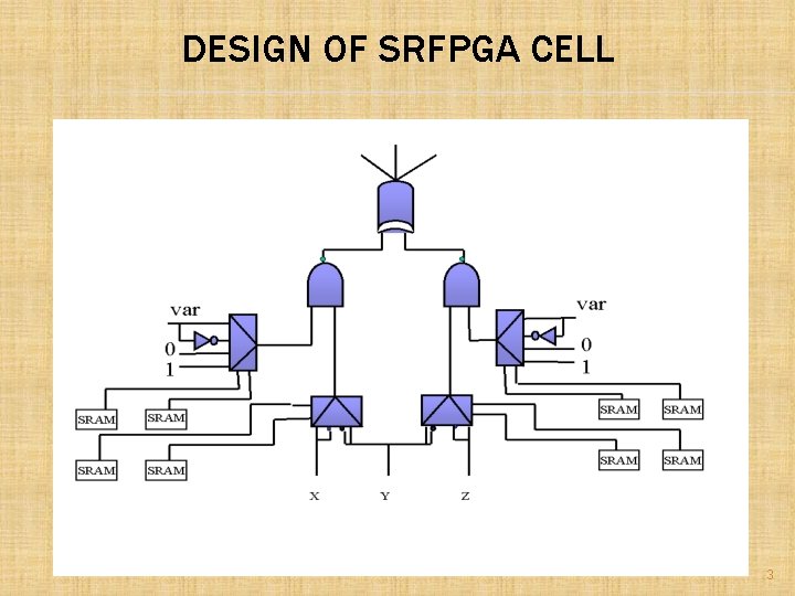
DESIGN OF SRFPGA CELL 3

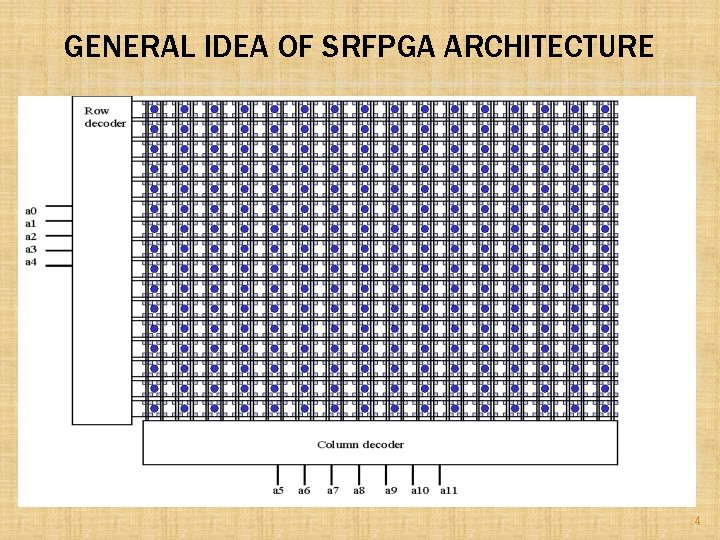
GENERAL IDEA OF SRFPGA ARCHITECTURE 4

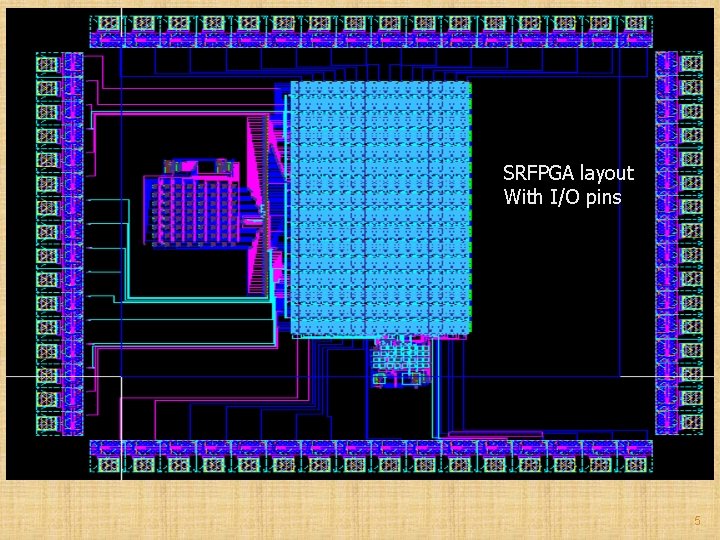
SRFPGA layout With I/O pins 5

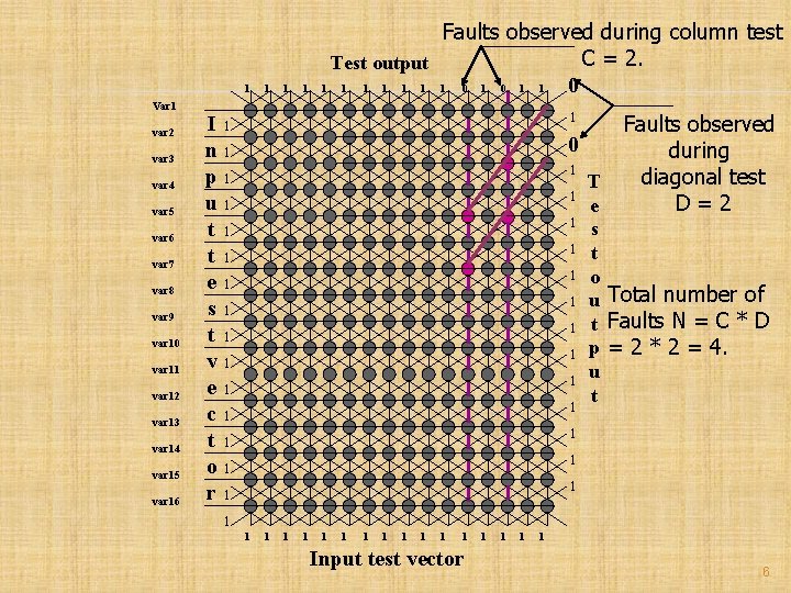
1 Var 1 var 2 var 3 var 4 var 5 var 6 var 7 var 8 var 9 var 10 var 11 var 12 var 13 var 14 var 15 var 16 1 1 1 Faults observed during column test C = 2. Test output 1 1 1 1 0 1 I 1 n 1 p 1 u 1 t 1 e 1 s 1 t 1 v 1 e 1 c 1 t 1 o 1 r 1 0 1 1 1 1 1 Faults observed during diagonal test D=2 T e s t o u Total number of t Faults N = C * D p = 2 * 2 = 4. u t 1 1 1 1 Input test vector 1 1 6

REVERSIBLE LOGIC 7

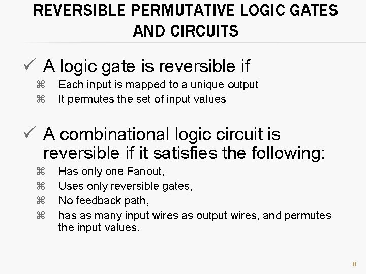
REVERSIBLE PERMUTATIVE LOGIC GATES AND CIRCUITS ü A logic gate is reversible if Each input is mapped to a unique output It permutes the set of input values ü A combinational logic circuit is reversible if it satisfies the following: Has only one Fanout, Uses only reversible gates, No feedback path, has as many input wires as output wires, and permutes the input values. 8

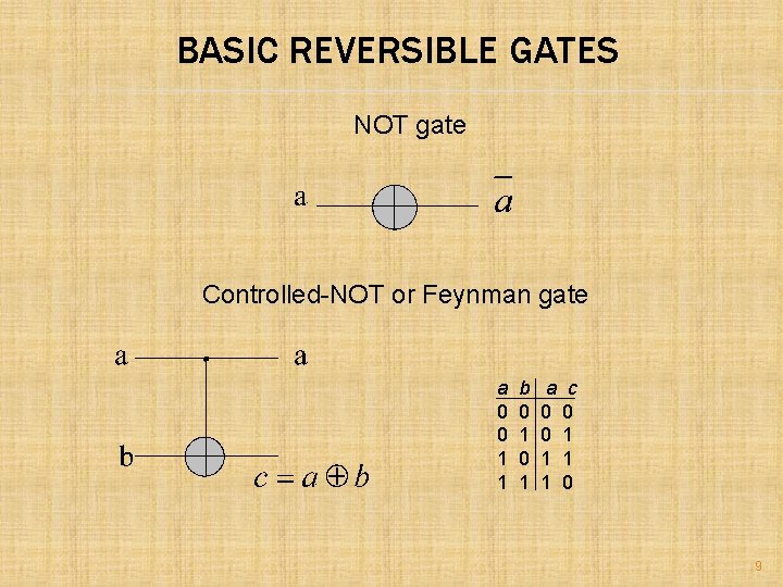
BASIC REVERSIBLE GATES NOT gate Controlled-NOT or Feynman gate a 0 0 1 1 b 0 1 a c 0 0 0 1 1 0 9

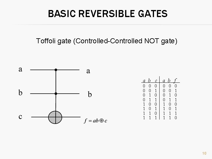
BASIC REVERSIBLE GATES Toffoli gate (Controlled-Controlled NOT gate) a b c a b f 0 0 0 0 1 1 1 1 0 0 1 1 0 1 0 1 1 0 10

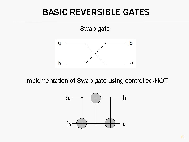
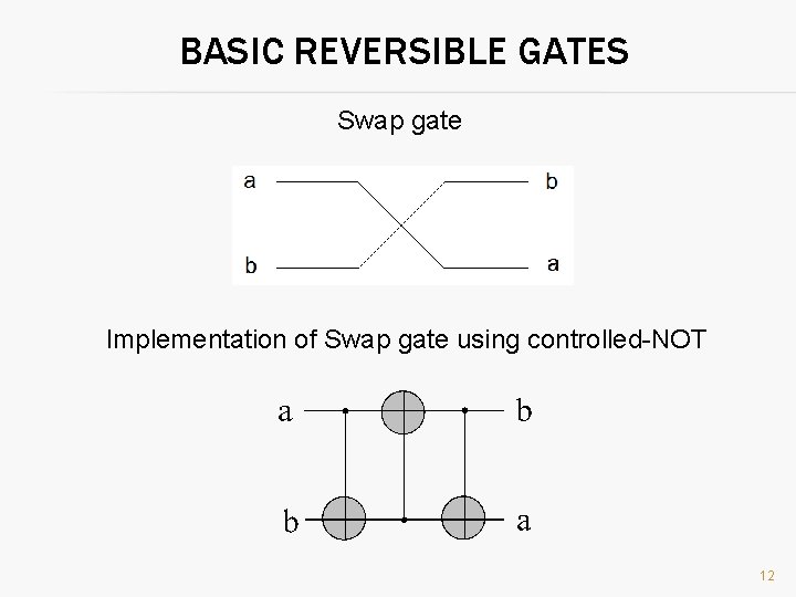
BASIC REVERSIBLE GATES Swap gate Implementation of Swap gate using controlled-NOT 11

BASIC REVERSIBLE GATES Swap gate Implementation of Swap gate using controlled-NOT 12

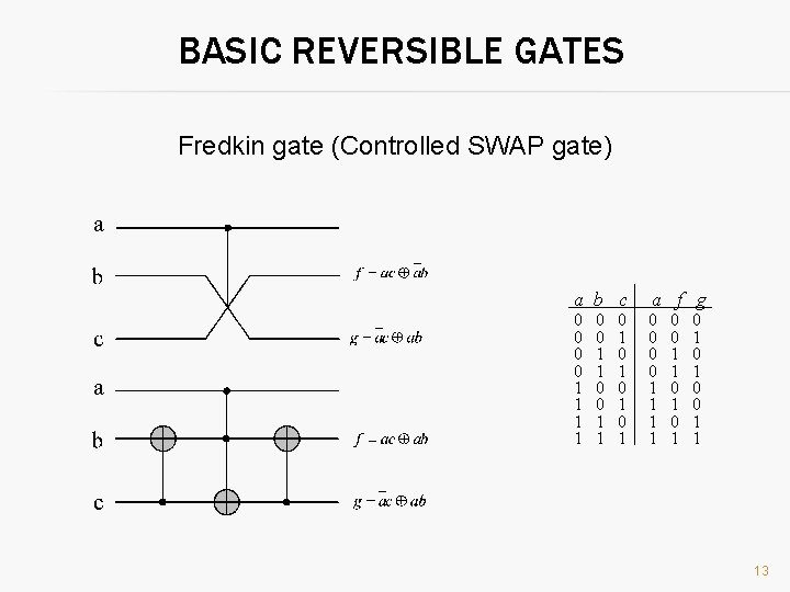
BASIC REVERSIBLE GATES Fredkin gate (Controlled SWAP gate) a b c a f g 0 0 0 0 1 1 1 1 0 0 1 1 0 1 0 1 0 0 1 1 13

ALGORITHMS FOR SYNTHESIS OF REVERSIBLE LOGIC CIRCUITS 14

POPULAR ALGORITHMS FOR SYNTHESIS OF REVERSIBLE LOGIC CIRCUITS ü MMD: Transformation based ü Gupta-Agrawal-Jha: PPRM based ü Mishchenko-Perkowski: Reversible wave cascade ü Kerntopf: Heuristics based ü Wille: BDD based synthesis 15

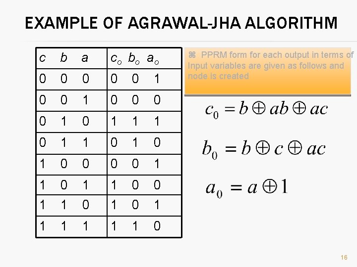
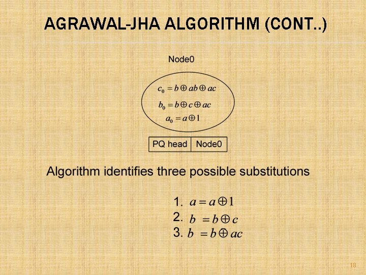
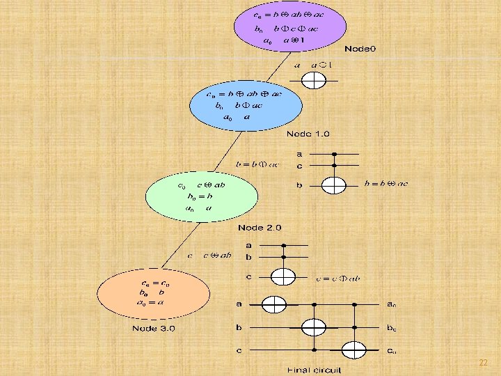
EXAMPLE OF AGRAWAL-JHA ALGORITHM c b a co bo ao 0 0 0 1 0 0 0 0 1 1 1 0 1 0 0 0 0 1 1 0 1 1 1 0 PPRM form for each output in terms of Input variables are given as follows and node is created 16

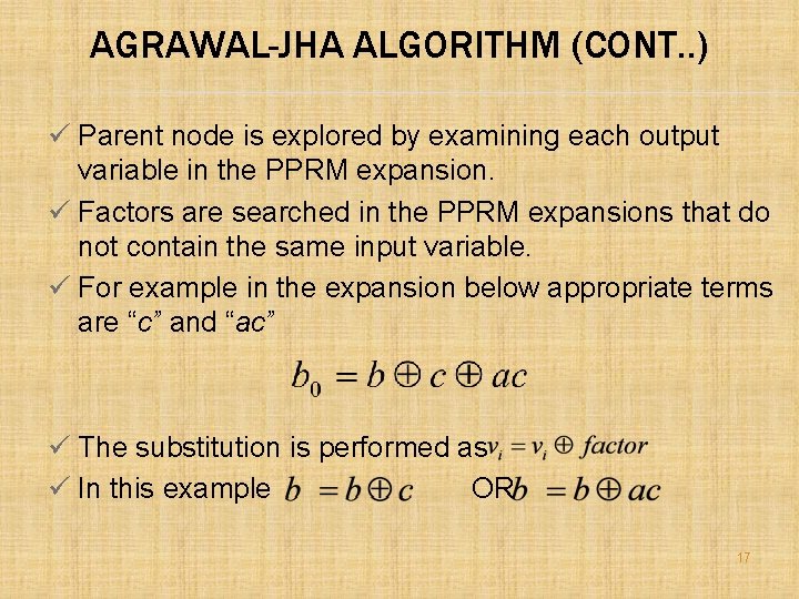
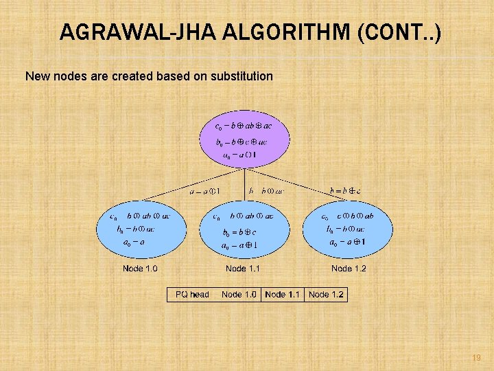
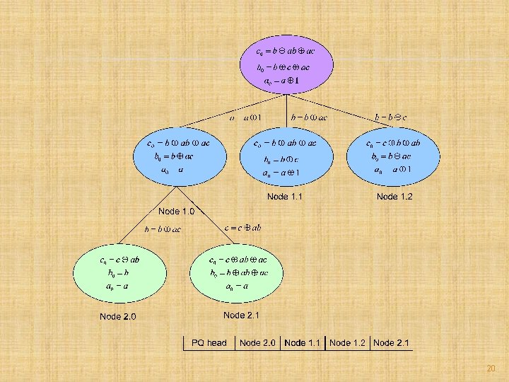
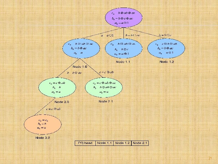
AGRAWAL-JHA ALGORITHM (CONT. . ) ü Parent node is explored by examining each output variable in the PPRM expansion. ü Factors are searched in the PPRM expansions that do not contain the same input variable. ü For example in the expansion below appropriate terms are “c” and “ac” ü The substitution is performed as ü In this example OR 17

AGRAWAL-JHA ALGORITHM (CONT. . ) 18

AGRAWAL-JHA ALGORITHM (CONT. . ) New nodes are created based on substitution 19

20

21

22

PROBLEM WITH CURRENT SYNTHESIS APPROACHES ü Common problem with current approaches: they invariably use nxn Toffoli gates, that might imposes technological limitations. ü High Quantum cost of Toffoli gates with many inputs. ü Synthesize only reversible functions, not Boolean functions that is not reversible. 23

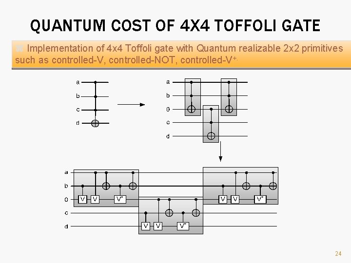
QUANTUM COST OF 4 X 4 TOFFOLI GATE Implementation of 4 x 4 Toffoli gate with Quantum realizable 2 x 2 primitives such as controlled-V, controlled-NOT, controlled-V+. 24

CREATING QUANTUM ARRAY FROM LATTICE 25

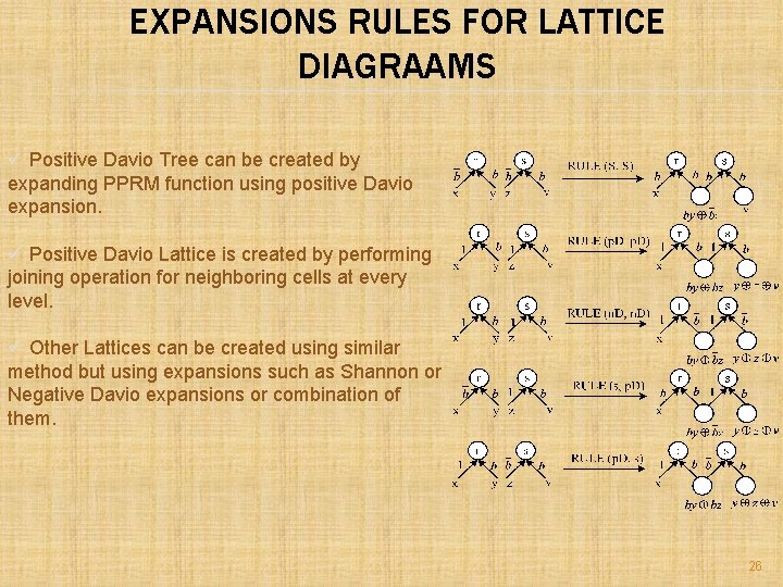
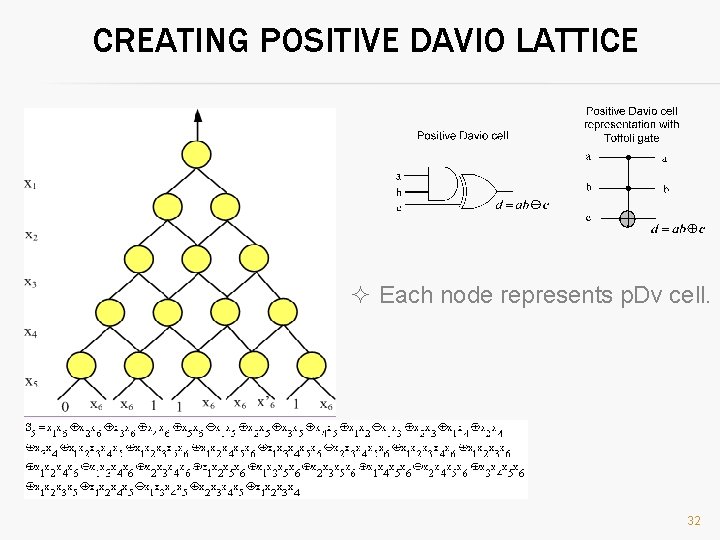
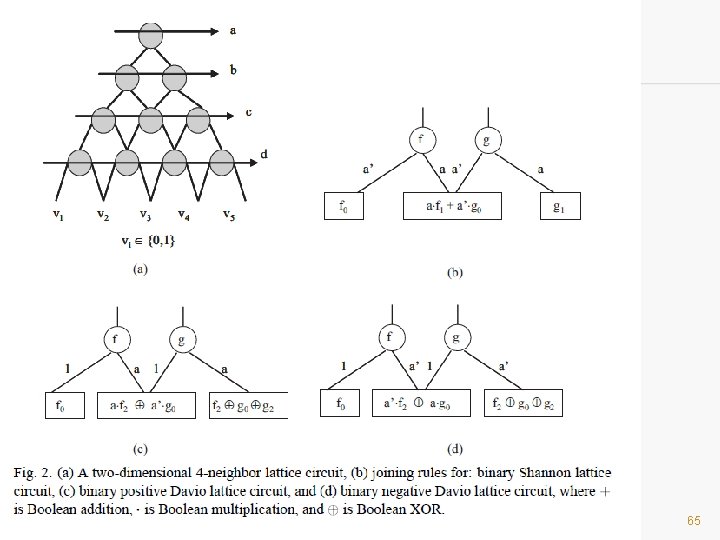
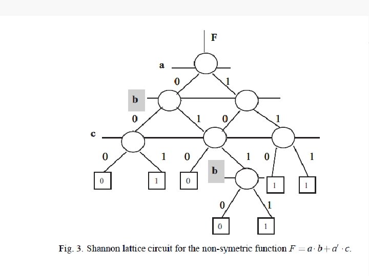
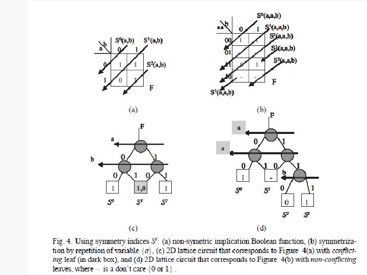
EXPANSIONS RULES FOR LATTICE DIAGRAAMS ü Positive Davio Tree can be created by expanding PPRM function using positive Davio expansion. ü Positive Davio Lattice is created by performing joining operation for neighboring cells at every level. ü Other Lattices can be created using similar method but using expansions such as Shannon or Negative Davio expansions or combination of them. 26

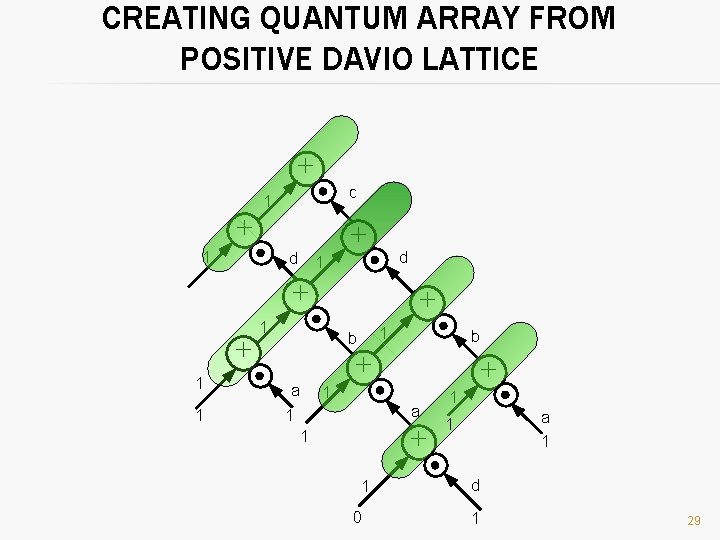
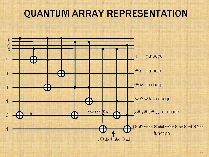
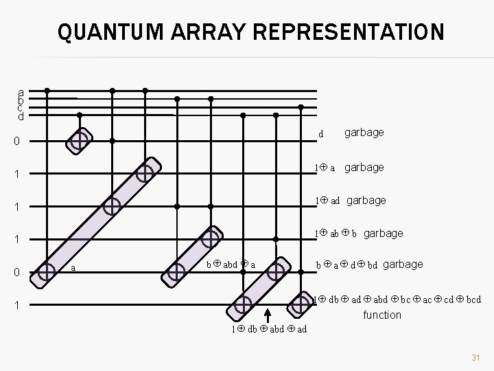
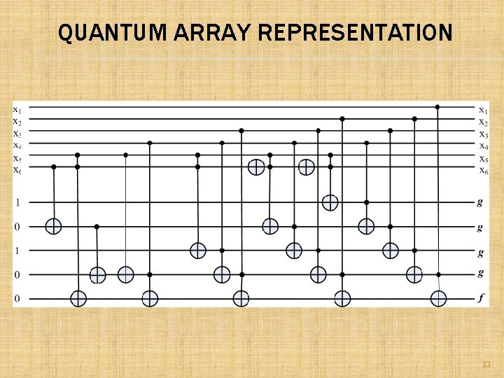
CREATING QUANTUM ARRAY FROM LATTICES ü On the previous foils I showed representation of the Davio and Shannon cells as cascade of reversible gates. ü Next I present unique method to create Quantum Array from Positive Davio Lattice. ü The same approach can be used for other Lattices. 27

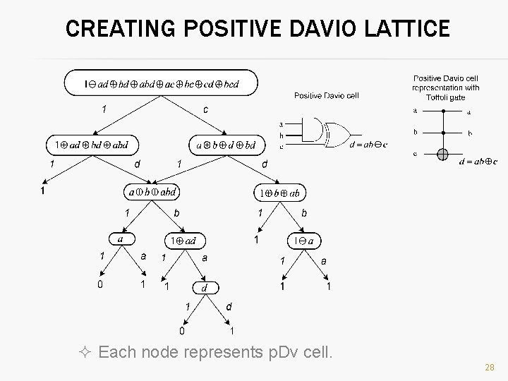
CREATING POSITIVE DAVIO LATTICE ² Each node represents p. Dv cell. 28

CREATING QUANTUM ARRAY FROM POSITIVE DAVIO LATTICE + + c 1 1 + d d 1 + + 1 1 b b + a + 1 a 1 + 1 1 0 1 a 1 1 d 1 29

QUANTUM ARRAY REPRESENTATION a b c d d 0 1 Å a garbage 1 1 Å ad garbage 1 1 Å ab Å b garbage 1 0 garbage a b Å abd Å a b Å a Å d Å bd garbage 1 Å db Å ad Å abd Å bc Å ac Å cd Å bcd 1 function 1 Å db Å abd Å ad 30

QUANTUM ARRAY REPRESENTATION a b c d d 0 1 Å a garbage 1 1 Å ad garbage 1 1 Å ab Å b garbage 1 0 garbage a b Å abd Å a b Å a Å d Å bd garbage 1 Å db Å ad Å abd Å bc Å ac Å cd Å bcd 1 function 1 Å db Å abd Å ad 31

CREATING POSITIVE DAVIO LATTICE ² Each node represents p. Dv cell. 32

QUANTUM ARRAY REPRESENTATION 33

ADVANTAGES OF LATTICE TO QA ü Reversible circuit synthesized with only 3 x 3 Toffoli gates. ü Generates reversible circuit for any ESOP. ü Adds ancilla bits but overall cost of the circuit will be lower due to use of low cost 3 x 3 Toffoli gates. 34

35

36

37

DIPAL GATES, DIPAL GATE FAMILIES AND THEIR 38

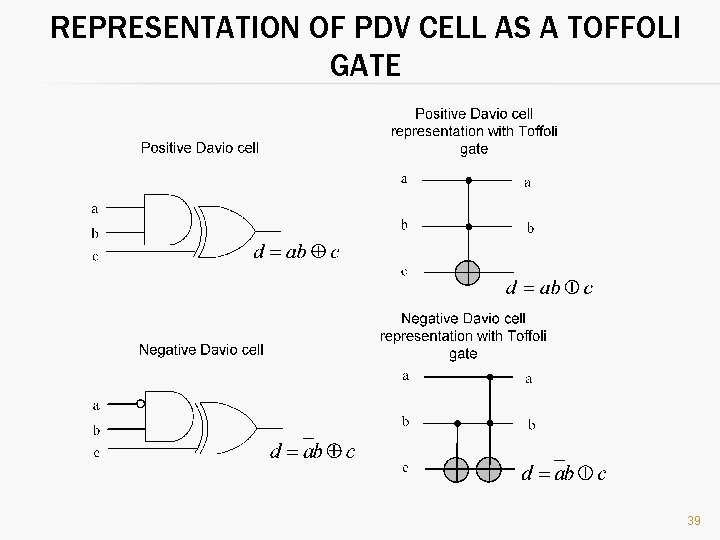
REPRESENTATION OF PDV CELL AS A TOFFOLI GATE 39

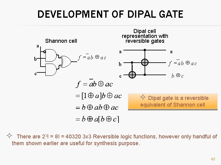
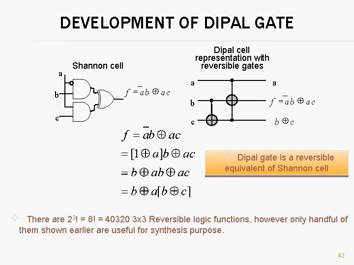
DEVELOPMENT OF DIPAL GATE a b c Dipal cell representation with reversible gates Shannon cell f =ab Åac a a b f =ab Åac c b Åc ² Dipal gate is a reversible equivalent of Shannon cell ² There are 23! = 8! = 40320 3 x 3 Reversible logic functions, however only handful of them shown earlier are useful for synthesis purpose. 40

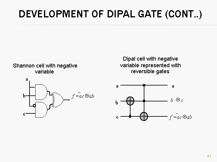
DEVELOPMENT OF DIPAL GATE (CONT. . ) Dipal cell with negative variable represented with reversible gates Shannon cell with negative variable a b c a a b b Åc c f =ac Åab 41

DEVELOPMENT OF DIPAL GATE a b c Dipal cell representation with reversible gates Shannon cell f =ab Åac a a b f =ab Åac c b Åc ² Dipal gate is a reversible equivalent of Shannon cell ² There are 23! = 8! = 40320 3 x 3 Reversible logic functions, however only handful of them shown earlier are useful for synthesis purpose. 42

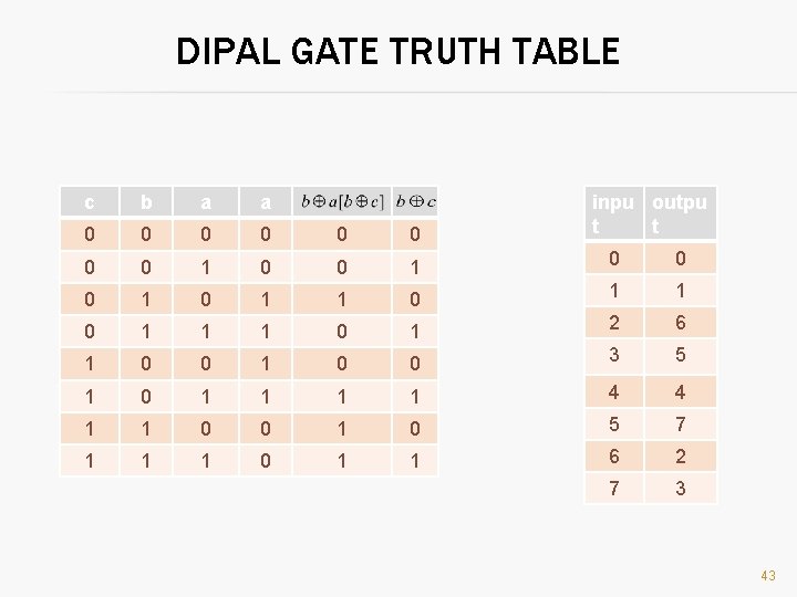
DIPAL GATE TRUTH TABLE c b a a 0 0 0 0 1 1 0 1 1 1 0 1 2 6 1 0 0 3 5 1 0 1 1 4 4 1 1 0 0 1 0 5 7 1 1 1 0 1 1 6 2 7 3 inpu outpu t t 43

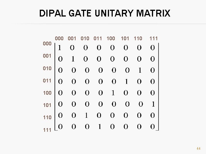
DIPAL GATE UNITARY MATRIX 000 001 010 011 100 101 110 111 44

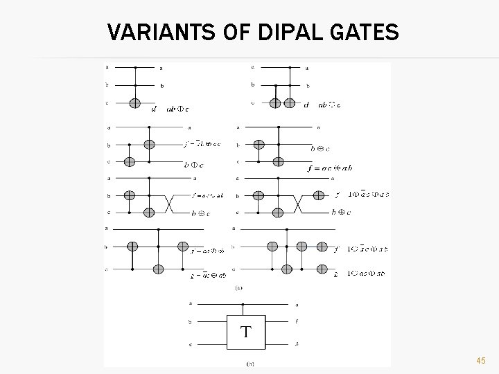
VARIANTS OF DIPAL GATES 45

EXPERIMENT AL RESULTS 46

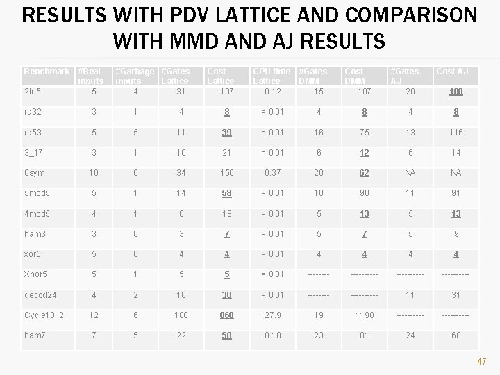
RESULTS WITH PDV LATTICE AND COMPARISON WITH MMD AND AJ RESULTS Benchmark 2 to 5 #Real inputs 5 #Garbage #Gates inputs Lattice 4 31 Cost Lattice 107 CPU time Lattice 0. 12 #Gates DMM 15 Cost DMM 107 #Gates AJ 20 Cost AJ 100 rd 32 3 1 4 8 < 0. 01 4 8 rd 53 5 5 11 39 < 0. 01 16 75 13 116 3_17 3 1 10 21 < 0. 01 6 12 6 14 6 sym 10 6 34 150 0. 37 20 62 NA NA 5 mod 5 5 1 14 58 < 0. 01 10 90 11 91 4 mod 5 4 1 6 18 < 0. 01 5 13 ham 3 3 0 3 7 < 0. 01 5 7 5 9 xor 5 5 0 4 4 < 0. 01 4 4 Xnor 5 5 1 5 5 < 0. 01 ---------- decod 24 4 2 10 30 < 0. 01 ---------- 11 31 Cycle 10_2 12 6 180 860 27. 9 19 1198 ---------- ham 7 7 5 22 58 0. 10 23 81 24 68 47

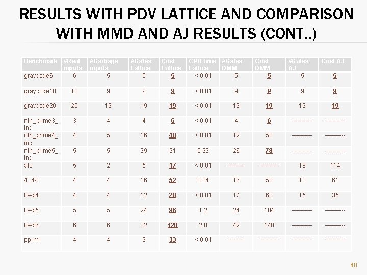
RESULTS WITH PDV LATTICE AND COMPARISON WITH MMD AND AJ RESULTS (CONT. . ) Benchmark graycode 6 #Real inputs 6 #Garbage inputs 5 #Gates Lattice 5 Cost Lattice 5 CPU time #Gates Lattice DMM < 0. 01 5 Cost DMM 5 #Gates AJ 5 Cost AJ graycode 10 10 9 9 9 < 0. 01 9 9 graycode 20 20 19 19 19 < 0. 01 19 19 nth_prime 3_ inc nth_prime 4_ inc nth_prime 5_ inc alu 3 4 4 6 < 0. 01 4 6 ---------- 4 5 16 48 < 0. 01 12 58 ---------- 5 5 29 91 0. 22 26 78 ---------- 5 2 5 17 < 0. 01 ---------- 18 114 4_49 4 4 16 52 0. 04 16 58 13 61 hwb 4 4 4 12 28 < 0. 01 17 63 15 35 hwb 5 5 5 24 96 1. 2 24 104 ---------- hwb 6 6 6 32 128 2. 0 42 140 ---------- pprm 1 4 4 9 33 < 0. 01 ---------- 5 48

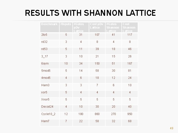
RESULTS WITH SHANNON LATTICE Benchmark 2 to 5 #Inputs #Gates p. Dv Lattice 5 31 Cost p. Dv Lattice 107 #Gates Shannon Lattice 41 Cost Shannon Lattice 117 rd 32 3 4 8 rd 53 5 11 39 18 46 3_17 3 10 21 15 26 6 sym 10 34 150 51 167 5 mod 5 5 14 58 30 81 4 mod 5 4 6 18 12 24 Ham 3 3 3 7 6 10 xor 5 5 4 4 Xnor 5 5 5 Decod 24 4 10 30 20 40 Cycle 10_2 12 180 860 270 950 Ham 7 7 22 58 32 68 49

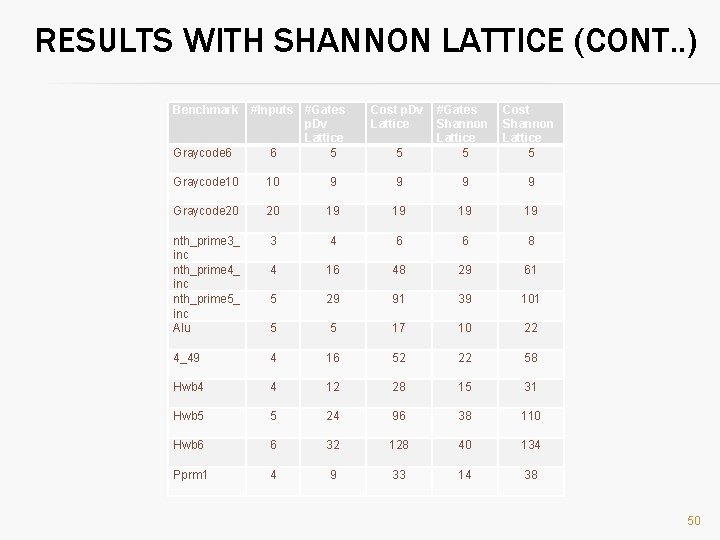
RESULTS WITH SHANNON LATTICE (CONT. . ) Benchmark Graycode 6 #Inputs #Gates p. Dv Lattice 6 5 Cost p. Dv Lattice 5 #Gates Shannon Lattice 5 Cost Shannon Lattice 5 Graycode 10 10 9 9 Graycode 20 20 19 19 nth_prime 3_ inc nth_prime 4_ inc nth_prime 5_ inc Alu 3 4 6 6 8 4 16 48 29 61 5 29 91 39 101 5 5 17 10 22 4_49 4 16 52 22 58 Hwb 4 4 12 28 15 31 Hwb 5 5 24 96 38 110 Hwb 6 6 32 128 40 134 Pprm 1 4 9 33 14 38 50

51

52

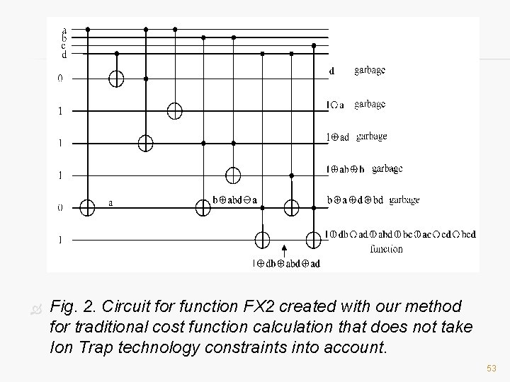
Fig. 2. Circuit for function FX 2 created with our method for traditional cost function calculation that does not take Ion Trap technology constraints into account. 53

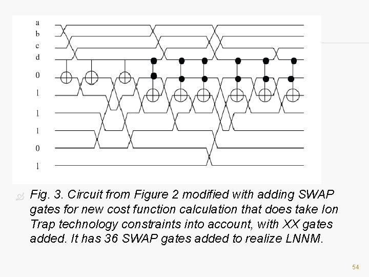
Fig. 3. Circuit from Figure 2 modified with adding SWAP gates for new cost function calculation that does take Ion Trap technology constraints into account, with XX gates added. It has 36 SWAP gates added to realize LNNM. 54
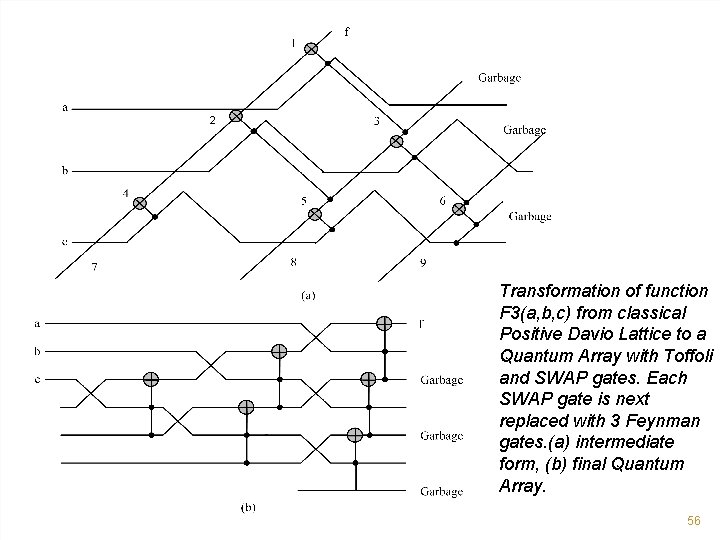
![Example of Positive Davio Lattice from Perkowski 97 d Positive Davio Expansion is applied Example of Positive Davio Lattice from [Perkowski 97 d]. Positive Davio Expansion is applied](https://slidetodoc.com/presentation_image_h2/e21803d3fa08f66dd6a9ffe55e10974a/image-55.jpg)
Example of Positive Davio Lattice from [Perkowski 97 d]. Positive Davio Expansion is applied in 55 each node. Variable d is repeated

Transformation of function F 3(a, b, c) from classical Positive Davio Lattice to a Quantum Array with Toffoli and SWAP gates. Each SWAP gate is next replaced with 3 Feynman gates. (a) intermediate form, (b) final Quantum Array. 56

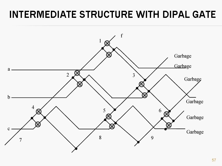
INTERMEDIATE STRUCTURE WITH DIPAL GATE 57

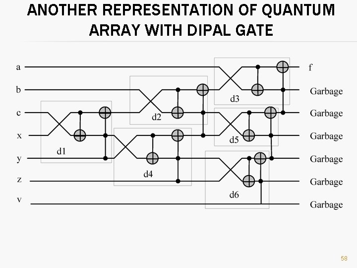
ANOTHER REPRESENTATION OF QUANTUM ARRAY WITH DIPAL GATE 58

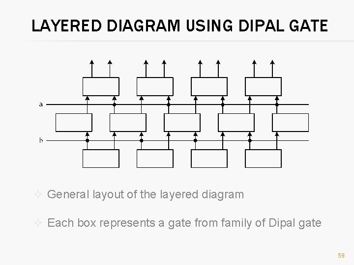
LAYERED DIAGRAM USING DIPAL GATE ² General layout of the layered diagram ² Each box represents a gate from family of Dipal gate 59

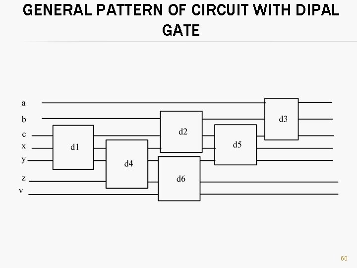
GENERAL PATTERN OF CIRCUIT WITH DIPAL GATE 60

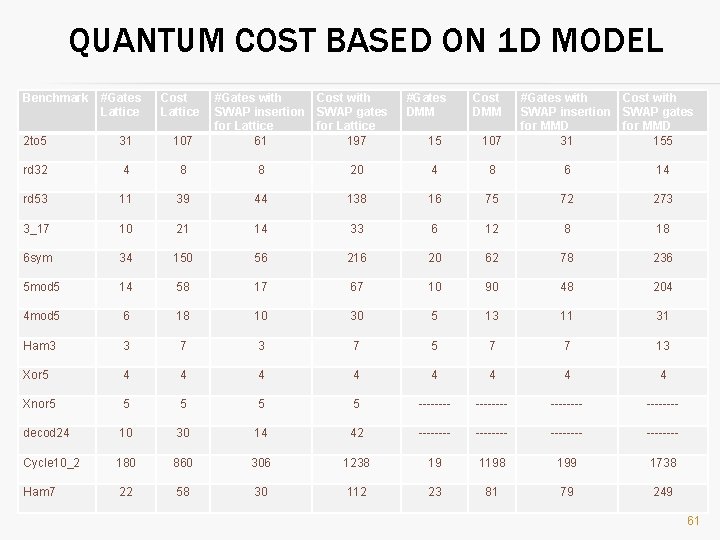
QUANTUM COST BASED ON 1 D MODEL Benchmark #Gates Lattice Cost Lattice 2 to 5 31 107 #Gates with SWAP insertion for Lattice 61 rd 32 4 8 8 rd 53 11 39 3_17 10 6 sym Cost with SWAP gates for Lattice 197 #Gates DMM Cost DMM 15 107 #Gates with SWAP insertion for MMD 31 Cost with SWAP gates for MMD 155 20 4 8 6 14 44 138 16 75 72 273 21 14 33 6 12 8 18 34 150 56 216 20 62 78 236 5 mod 5 14 58 17 67 10 90 48 204 4 mod 5 6 18 10 30 5 13 11 31 Ham 3 3 7 5 7 7 13 Xor 5 4 4 4 4 Xnor 5 5 5 -------- decod 24 10 30 14 42 -------- Cycle 10_2 180 860 306 1238 19 1198 199 1738 Ham 7 22 58 30 112 23 81 79 249 61

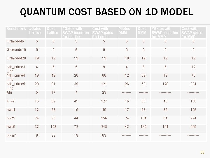
QUANTUM COST BASED ON 1 D MODEL Benchmark #Gates Lattice Cost Lattice Graycode 6 5 5 #Gates with SWAP insertion for Lattice 5 Graycode 10 9 9 9 Graycode 20 19 19 Nth_prime 3 _inc Nth_prime 4 _inc Nth_prime 5 _inc Alu 4 Cost with SWAP gates for Lattice 5 #Gates DMM Cost DMM 5 5 #Gates with SWAP insertion for MMD 5 Cost with SWAP gates for MMD 5 9 9 9 19 19 19 6 5 9 4 6 6 12 16 48 20 60 12 58 18 76 29 91 39 121 26 78 128 384 5 17 7 23 ---------- 4_49 16 52 41 127 16 58 40 130 hwb 4 12 28 15 40 17 63 39 129 hwb 5 24 96 44 156 24 104 64 224 hwb 6 32 128 72 248 42 140 144 446 pprm 1 9 33 19 63 ---------- 62

GENERALIZED REGULARITIES FOR QUANTUM AND NANOTECHNOLOGIES 63

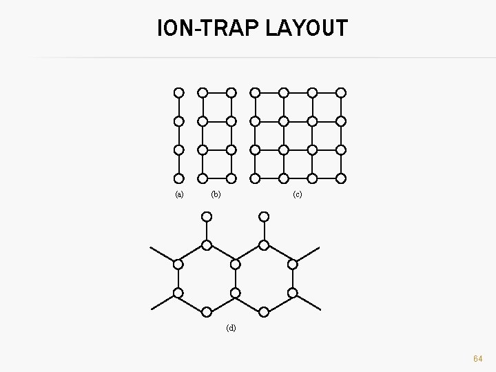
ION-TRAP LAYOUT (a) (b) (c) (d) 64

65

66

67

68

69

70

71

72

73

QUANTUM CIRCUITS AND QUANTUM ARRAYS FROM TRULY QUANTUM 74

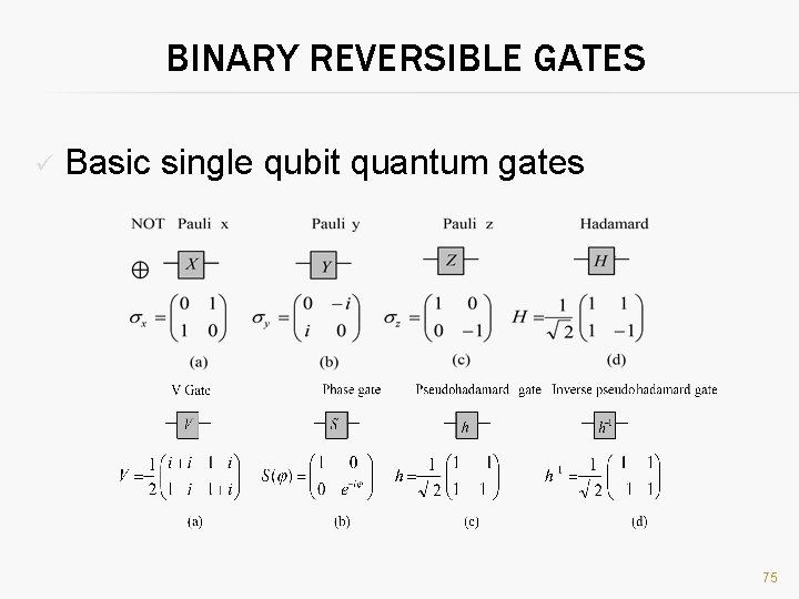
BINARY REVERSIBLE GATES ü Basic single qubit quantum gates 75

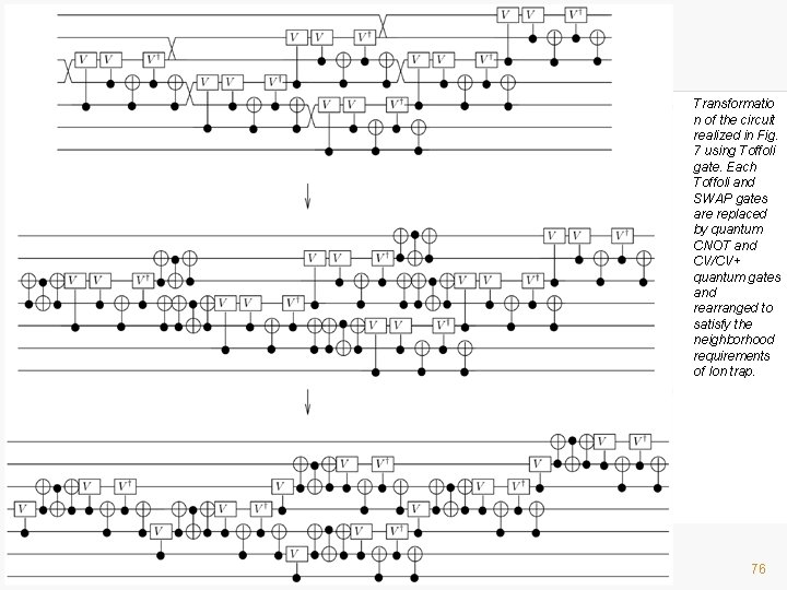
Transformatio n of the circuit realized in Fig. 7 using Toffoli gate. Each Toffoli and SWAP gates are replaced by quantum CNOT and CV/CV+ quantum gates and rearranged to satisfy the neighborhood requirements of Ion trap. 76

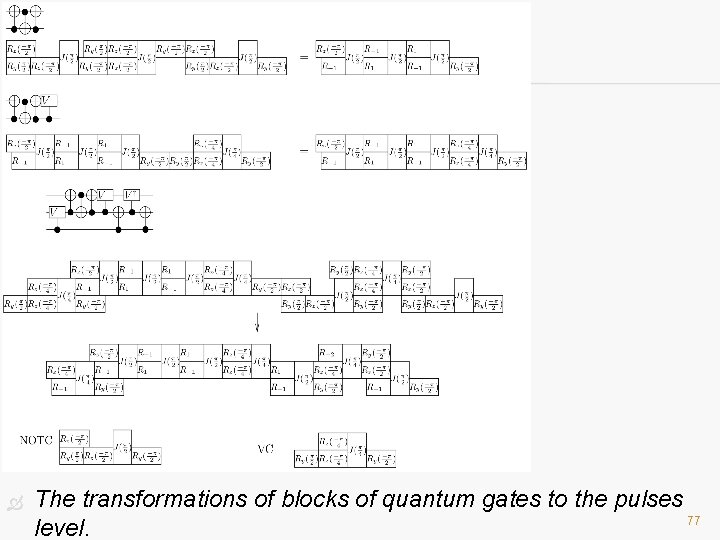
The transformations of blocks of quantum gates to the pulses 77 level.

CONCLUSION S 78

CONCLUSIONS ü Experimental results proved that our algorithm produced better results in terms of quantum cost compared to other contemporary algorithms for synthesis of reversible logic. ü New gate family called Dipal gate ü Presented new synthesis method with layered diagrams. ü ü More accurate technology specific cost model for 1 D qubit neighborhood architecture. 79

CONCLUSIONS ü A new method based of lattice diagram to synthesize reversible logic circuit with 3 x 3 Toffoli gates. ü A new family of gates called Dipal Gates. ü New diagrams called layered diagram that uses family of Dipal gate for synthesis of reversible logic function. ü Software for creating Lattice diagrams and software for creating quantum array from Lattice (Lattice to QA). ü Program to implement a variant of MMD algorithm. 80