Design of Flexible Printed Circuit Prototype towards RD
Design of Flexible Printed Circuit Prototype towards RD 53 IC Ilya Tsurin Liverpool University on behalf of ATLAS UK WP 1/WP 2 18/09/2017 ATLAS ITk week 1
Design Objectives Re-design of the FE-I 4 B Quad hybrid (with the RD 53 chip in mind) for the new version of the Pixel End. Cap bus tape Full System Test for Pixel TDR: Mechanical concepts, connectivity, power distribution, cooling, readout, sensor performance, characterization of stresses and lifetime etc. Drafting solutions for the RD 53 IC Quad hybrid Power density, readout speed, material budget, radiation tolerance etc. Elaborating Module Production Schedule Testing QC/QA procedures, infrastructure development 18/09/2017 ATLAS ITk week 2
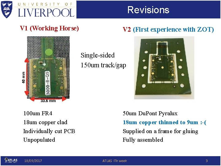
Revisions V 1 (Working Horse) V 2 (First experience with ZOT) Single-sided 150 um track/gap 100 um FR 4 18 um copper clad Individually cut PCB Unpopulated 18/09/2017 50 um Du. Pont Pyralux 18 um copper thinned to 9 um : -( Supplied on a frame for gluing Fully assembled ATLAS ITk week 3
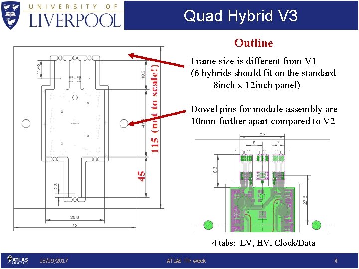
Quad Hybrid V 3 Outline Frame size is different from V 1 (6 hybrids should fit on the standard 8 inch x 12 inch panel) Dowel pins for module assembly are 10 mm further apart compared to V 2 4 tabs: LV, HV, Clock/Data 18/09/2017 ATLAS ITk week 4
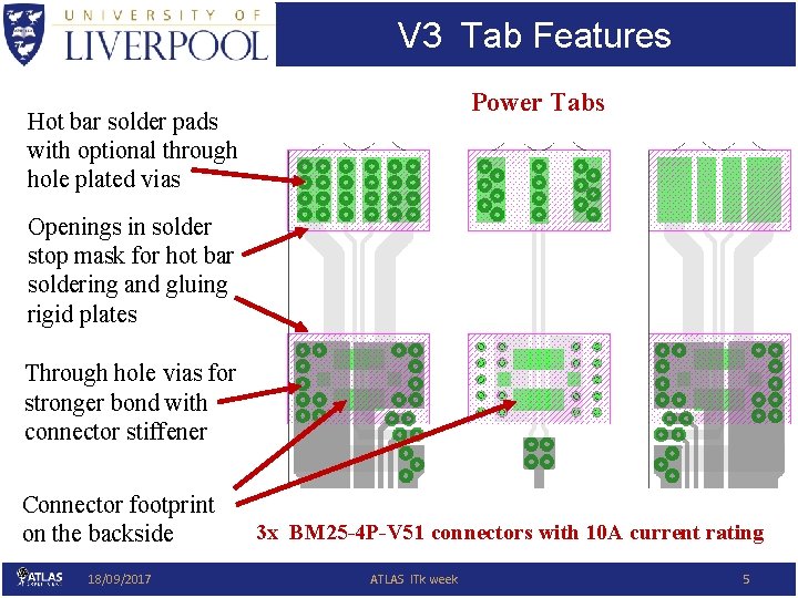
V 3 Tab Features Power Tabs Hot bar solder pads with optional through hole plated vias Openings in solder stop mask for hot bar soldering and gluing rigid plates Through hole vias for stronger bond with connector stiffener Connector footprint on the backside 18/09/2017 3 x BM 25 -4 P-V 51 connectors with 10 A current rating ATLAS ITk week 5

V 3 Power Connector Pinout Shield HV return GND VIN NTC+ HV VIN NTCGND - “HV return” referred to GND via RC high pass filter - “Shield” referred to GND via capacitor 18/09/2017 ATLAS ITk week 6
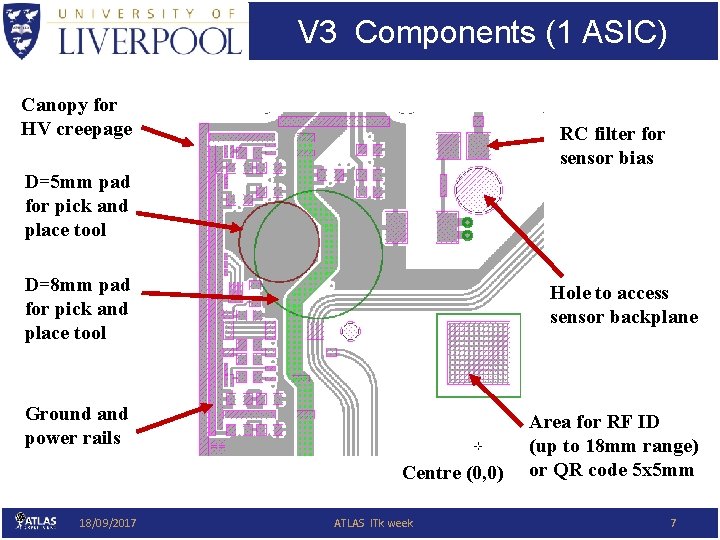
V 3 Components (1 ASIC) Canopy for HV creepage RC filter for sensor bias D=5 mm pad for pick and place tool D=8 mm pad for pick and place tool Hole to access sensor backplane Ground and power rails Area for RF ID (up to 18 mm range) or QR code 5 x 5 mm Centre (0, 0) 18/09/2017 ATLAS ITk week 7

V 3 Components (1 ASIC) “Beefy” Serial Power IN (selectively plated together with vias) Wire bond pads for connector-less integration Clock and command GA jumpers Opening for laser alignment of silicon sensor Alignment mark and bond-off pad Data Out (AC-coupled) Centre (0, 0) 18/09/2017 ATLAS ITk week 8
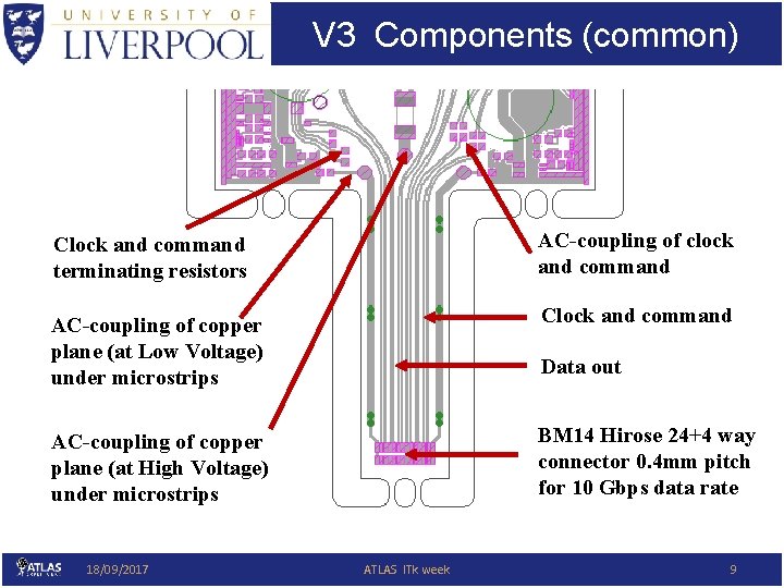
V 3 Components (common) Clock and command terminating resistors AC-coupling of clock and command AC-coupling of copper plane (at Low Voltage) under microstrips Clock and command Data out BM 14 Hirose 24+4 way connector 0. 4 mm pitch for 10 Gbps data rate AC-coupling of copper plane (at High Voltage) under microstrips 18/09/2017 ATLAS ITk week 9
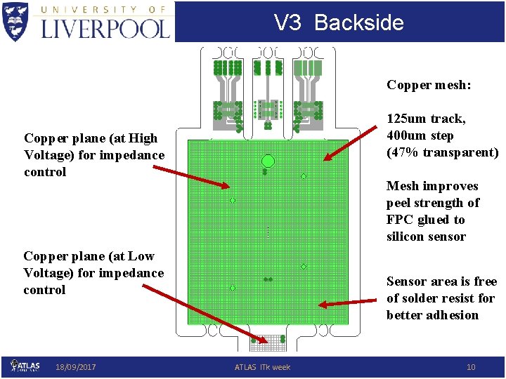
V 3 Backside Copper mesh: 125 um track, 400 um step (47% transparent) Copper plane (at High Voltage) for impedance control Mesh improves peel strength of FPC glued to silicon sensor Copper plane (at Low Voltage) for impedance control 18/09/2017 Sensor area is free of solder resist for better adhesion ATLAS ITk week 10
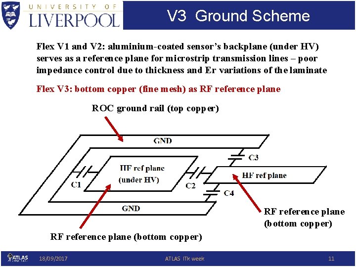
V 3 Ground Scheme Flex V 1 and V 2: aluminium-coated sensor’s backplane (under HV) serves as a reference plane for microstrip transmission lines – poor impedance control due to thickness and Er variations of the laminate Flex V 3: bottom copper (fine mesh) as RF reference plane ROC ground rail (top copper) RF reference plane (bottom copper) 18/09/2017 ATLAS ITk week 11
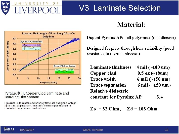
V 3 Laminate Selection Material: Dupont Pyralux AP: all polyimide (no adhesive) Designed for plate through hole reliability (good resistance to thermal stresses) Laminate thickness 4 mil (~100 um) Copper clad 0. 5 oz (~18 um) Trace width 6 mil (~150 um) Trace separation 6 mil (~150 um) Relative dielectric constant for Pyralux AP 3. 4 Zo = 32 Ohm, 18/09/2017 ATLAS ITk week Zd = 103 Ohm 12
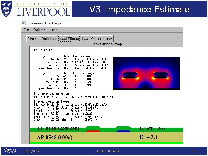
V 3 Impedance Estimate 18/09/2017 ATLAS ITk week 13
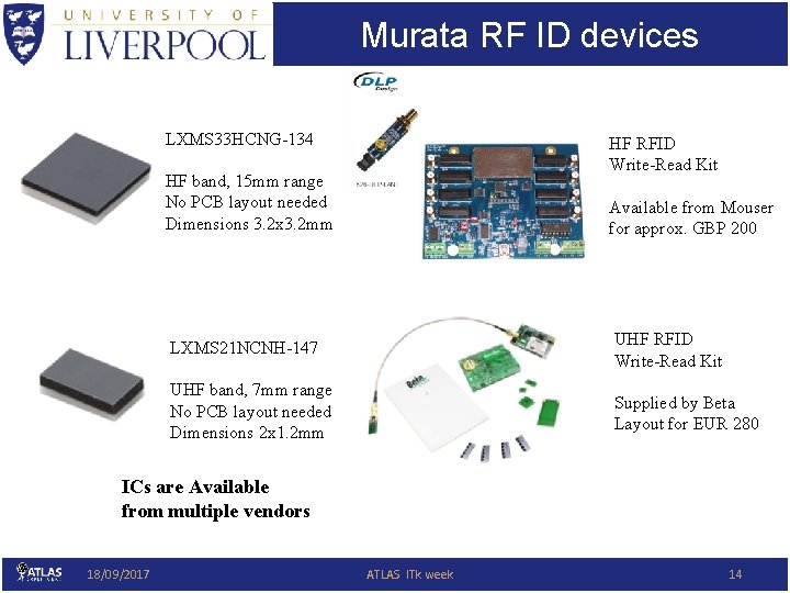
Murata RF ID devices LXMS 33 HCNG-134 HF RFID Write-Read Kit HF band, 15 mm range No PCB layout needed Dimensions 3. 2 x 3. 2 mm Available from Mouser for approx. GBP 200 LXMS 21 NCNH-147 UHF RFID Write-Read Kit UHF band, 7 mm range No PCB layout needed Dimensions 2 x 1. 2 mm Supplied by Beta Layout for EUR 280 ICs are Available from multiple vendors 18/09/2017 ATLAS ITk week 14
Summary 80 hybrids submitted with ZOT Plans to submit 10 hybrids with Stevenage to compare vendors for Pixel TDR Quad silicon packages (4 x. FE-I 4 B bump-bonded to “n-in-p” sensors ) are coming soon Reminder to organise UK/international Face-to-Face meeting for the module assembly (gluing FPC on silicon) 27/06/2017 ATLAS ITk week 15
Backup Slide 1 FPC specs: Double clad Du. Pont Pyralux AP 8545 (18 u copper, 100 u laminate), 150 u track and gap, 0. 3 mm minimum drill diameter, ENIG finish Top and bottom HXC 1215 coverlay (12 u polyimide film, 15 u epoxy adhesive) silkscreen print, individually cut, cleaned and packaged. Questions to FPC suppliers: 1. Stock availability / lead time of AP 8545 / HXC 1215 2. ENIG finish: total copper coverage / exposed contacts only (influence of ferromagnetic Nickel on properties of microstrips) 3. Selective via plating capabilities 4. Impedance control capabilities. 5. Etch control: dummy pattern in copper-free areas (radiation length) 27/06/2017 ATLAS ITk week 16
Backup Slide 2 FPC population 1. Compensating solder paste mask (provided) for kapton stretching 2. Ensure the right component grade (sulphur-free resistors, tolerance etc. ) 3. Leaded solder assembly (to avoid tin whiskers and tin pest) 4. Positioning accuracy of in-line connectors 5. Making use of RF ID chip Quality control 1. Visual inspection: solder escape to wire bond pads and misalignment of coverlay are unacceptable 2. Electrical test (flying leads): integrity of traces - discontinuities and shorts are unacceptable 3. Optical / tactile (CMM) inspection of ENIG finish for wire bonding, too rough (grainy) is unacceptable (probably an artefact of copper thinning) 4. Impedance measurements of microstrip transmission lines (PCB itself or test coupons). 27/06/2017 ATLAS ITk week 17
Backup Slide 2 FPC cleaning Application specific evaluations should be performed for the chosen solder paste to identify if any remaining residue still needs to be removed from the boards in final production. Plasma cleaning is recommended as a final step. Packaging, shipping Cleanroom materials should be used for packaging individual circuits. The use of foil laminated mylar bags sealed in inert environment is recommended. Measures should be taken to prevent circuits from bending during their shipment. 27/06/2017 ATLAS ITk week 18
- Slides: 18