Design of Digital Circuits Lecture 5 Combinational Logic

Design of Digital Circuits Lecture 5: Combinational Logic II Prof. Onur Mutlu ETH Zurich Spring 2019 7 March 2019

Assignment: Required Lecture n Why study computer architecture? Video n Why is it important? Future Computing Architectures n Required Assignment n q q n Watch my inaugural lecture at ETH and understand it https: //www. youtube. com/watch? v=kgi. Zl. SOc. GFM Optional Assignment – for 1% extra credit q Write a 1 -page summary of the lecture n n What are your key takeaways? What did you learn? What did you like or dislike? Upload PDF file to Moodle – Deadline: Friday, March 15. 2
Assignment: Required Readings n Last+This week q Combinational Logic n n This+Next week q Hardware Description Languages and Verilog n q H&H Chapter 4 until 4. 3 and 4. 5 Sequential Logic n n P&P Chapter 3 until 3. 3 + H&H Chapter 2 P&P Chapter 3. 4 until end + H&H Chapter 3 in full By the end of next week, make sure you are done with q P&P Chapters 1 -3 + H&H Chapters 1 -4 3
Combinational Logic Circuits and Design 4
What We Will Learn Today? n Building blocks of modern computers q q Transistors Logic gates n Boolean algebra n Combinational circuits n n How to use Boolean algebra to represent combinational circuits Minimizing logic circuits (if time permits) 5
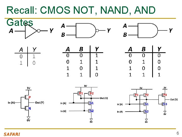
Recall: CMOS NOT, NAND, AND Gates 6
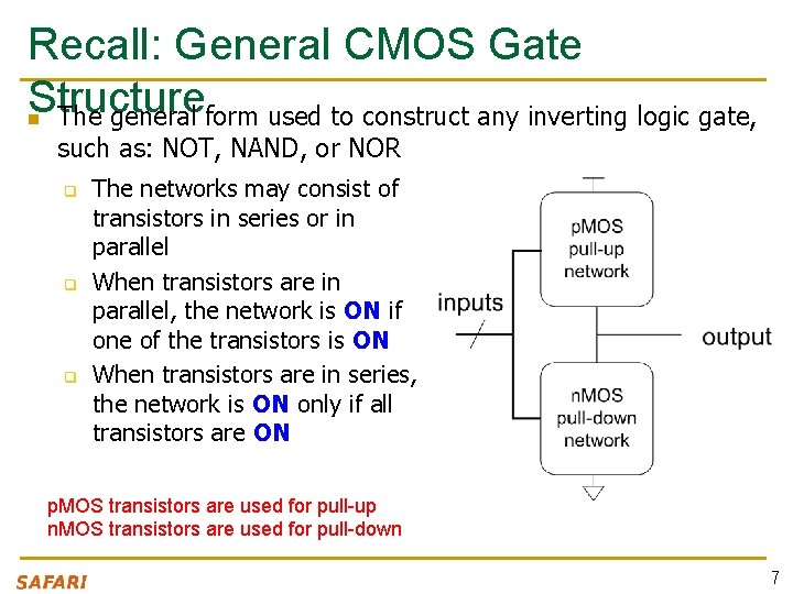
Recall: General CMOS Gate Structure n The general form used to construct any inverting logic gate, such as: NOT, NAND, or NOR q q q The networks may consist of transistors in series or in parallel When transistors are in parallel, the network is ON if one of the transistors is ON When transistors are in series, the network is ON only if all transistors are ON p. MOS transistors are used for pull-up n. MOS transistors are used for pull-down 7
Recall: Digging Deeper: Power Consumption n Dynamic Power Consumption q C * V 2 * f n n Static Power consumption q V * Ileakage n n supply voltage * leakage current Energy Consumption q n C = capacitance of the circuit (wires and gates) V = supply voltage f = charging frequency of the capacitor Power * Time See more in H&H Chapter 1. 8 8
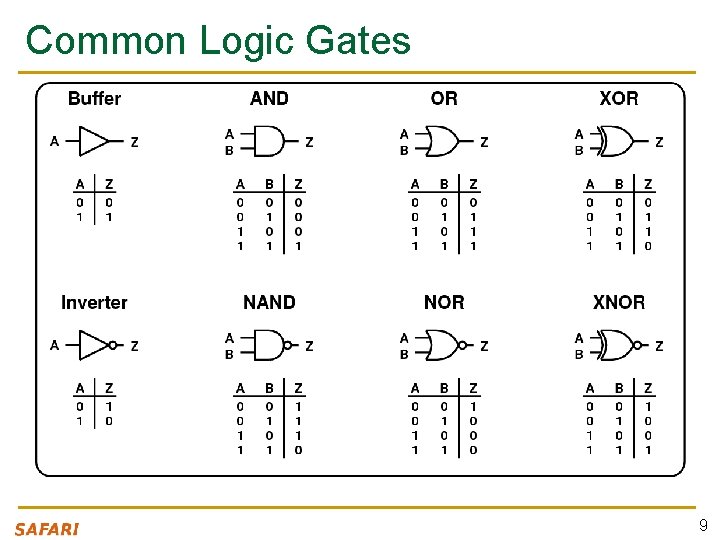
Common Logic Gates 9
Larger Gates n We can extend the gates to more than 2 inputs n Example: 3 -input AND gate, 10 -input NOR gate n See your readings 10
Aside: Moore’s Law: Enabler of Many Gates on a Chip 11
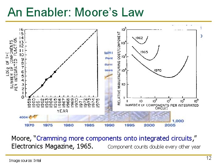
An Enabler: Moore’s Law Moore, “Cramming more components onto integrated circuits, ” Electronics Magazine, 1965. Component counts double every other year Image source: Intel 12
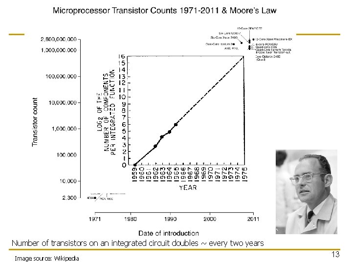
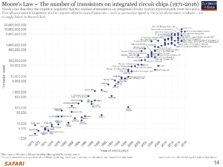
Number of transistors on an integrated circuit doubles ~ every two years Image source: Wikipedia 13
14
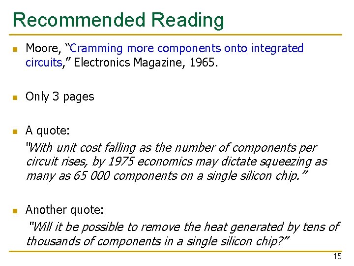
Recommended Reading n Moore, “Cramming more components onto integrated circuits, ” Electronics Magazine, 1965. n Only 3 pages n A quote: “With unit cost falling as the number of components per circuit rises, by 1975 economics may dictate squeezing as many as 65 000 components on a single silicon chip. ” Another quote: “Will it be possible to remove the heat generated by tens of n thousands of components in a single silicon chip? ” 15

How Do We Keep Moore’s Law n Manufacturing smaller transistors/structures q n Developing materials with better properties q q q n Copper instead of Aluminum (better conductor) Hafnium Oxide, air for Insulators Making sure all materials are compatible is the challenge Optimizing the manufacturing steps q n Some structures are already a few atoms in size How to use 193 nm ultraviolet light to pattern 20 nm structures New technologies q Fin. FET, Gate All Around transistor, Single Electron Transistor… 16

Combinational Logic Circuits 17
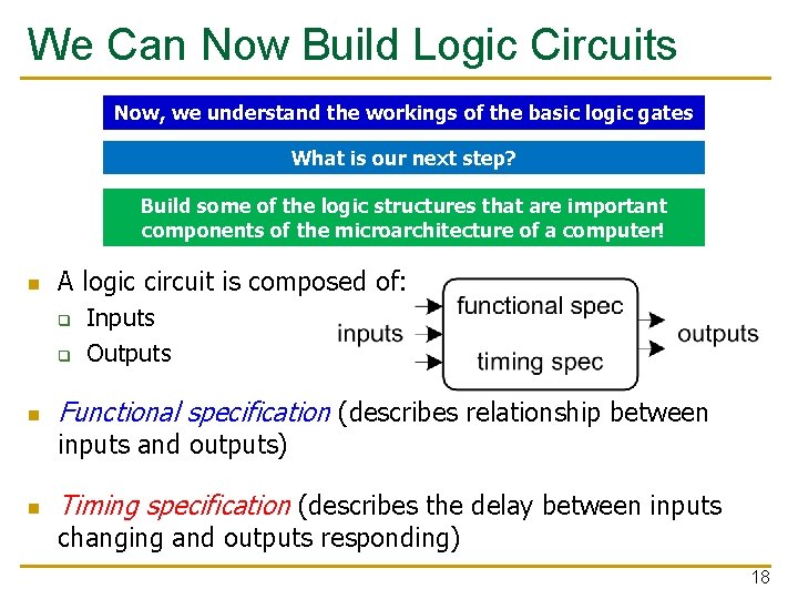
We Can Now Build Logic Circuits Now, we understand the workings of the basic logic gates What is our next step? Build some of the logic structures that are important components of the microarchitecture of a computer! n A logic circuit is composed of: q q n Inputs Outputs Functional specification (describes relationship between inputs and outputs) n Timing specification (describes the delay between inputs changing and outputs responding) 18

Types of Logic Circuits n Combinational Logic q q q n Memoryless Outputs are strictly dependent on the combination of input values that are being applied to circuit right now In some books called Combinatorial Logic Later we will learn: Sequential Logic q Has memory n q Structure stores history Can ”store” data values Outputs are determined by previous (historical) and current values of inputs 19
Boolean Equations 20
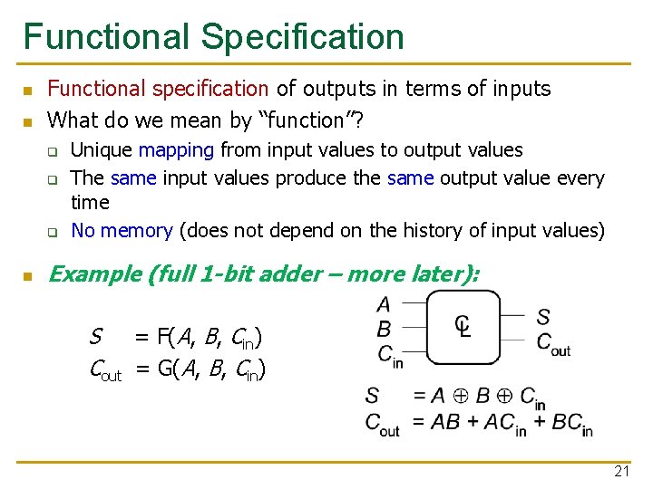
Functional Specification n n Functional specification of outputs in terms of inputs What do we mean by “function”? q q q n Unique mapping from input values to output values The same input values produce the same output value every time No memory (does not depend on the history of input values) Example (full 1 -bit adder – more later): S = F(A, B, Cin) Cout = G(A, B, Cin) 21
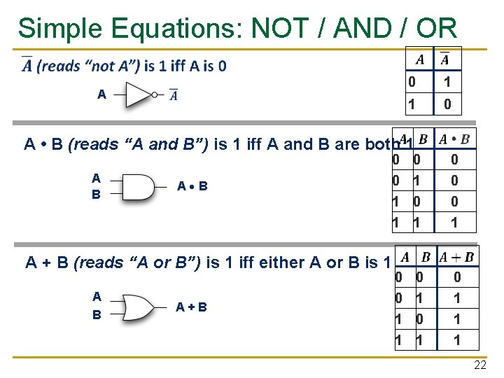
Simple Equations: NOT / AND / OR A 0 1 1 0 A • B (reads “A and B”) is 1 iff A and B are both 1 A B A · B 0 0 1 1 A + B (reads “A or B”) is 1 iff either A or B is 1 A B A + B 0 0 1 1 0 1 0 0 0 1 0 1 1 1 22
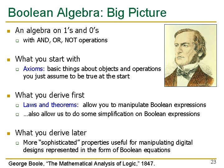
Boolean Algebra: Big Picture n An algebra on 1’s and 0’s q n What you start with q n Axioms: basic things about objects and operations you just assume to be true at the start What you derive first q q n with AND, OR, NOT operations Laws and theorems: allow you to manipulate Boolean expressions …also allow us to do some simplification on Boolean expressions What you derive later q More “sophisticated” properties useful for manipulating digital designs represented in the form of Boolean equations George Boole, “The Mathematical Analysis of Logic, ” 1847. 23
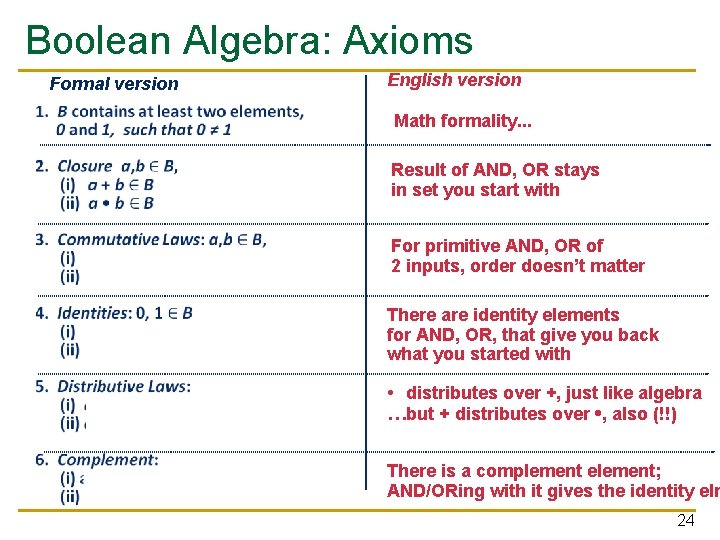
Boolean Algebra: Axioms Formal version English version Math formality. . . Result of AND, OR stays in set you start with For primitive AND, OR of 2 inputs, order doesn’t matter There are identity elements for AND, OR, that give you back what you started with • distributes over +, just like algebra …but + distributes over • , also (!!) There is a complement element; AND/ORing with it gives the identity elm 24
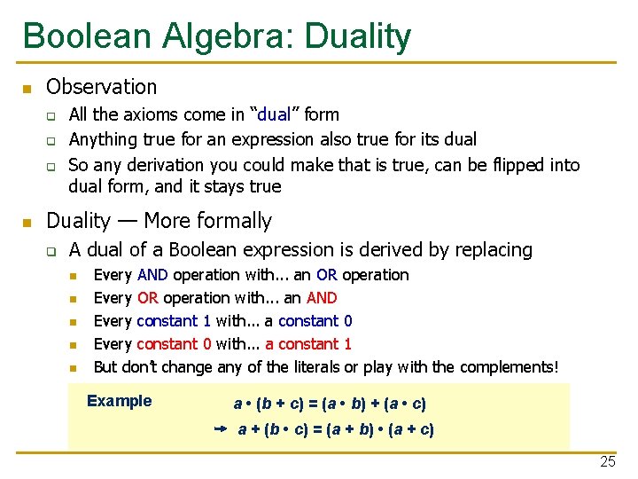
Boolean Algebra: Duality n Observation q q q n All the axioms come in “dual” form Anything true for an expression also true for its dual So any derivation you could make that is true, can be flipped into dual form, and it stays true Duality — More formally q A dual of a Boolean expression is derived by replacing n n n Every AND operation with. . . an OR operation Every OR operation with. . . an AND Every constant 1 with. . . a constant 0 Every constant 0 with. . . a constant 1 But don’t change any of the literals or play with the complements! Example a • (b + c) = (a • b) + (a • c) ➙ a + (b • c) = (a + b) • (a + c) 25
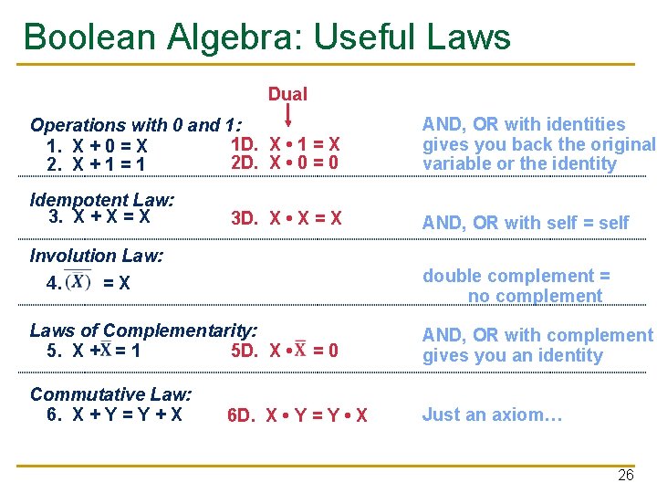
Boolean Algebra: Useful Laws Dual Operations with 0 and 1: 1 D. X • 1 = X 1. X + 0 = X 2 D. X • 0 = 0 2. X + 1 = 1 AND, OR with identities gives you back the original variable or the identity Idempotent Law: 3. X + X = X AND, OR with self = self 3 D. X • X = X Involution Law: double complement = no complement 4. = X Laws of Complementarity: 5. X + = 1 5 D. X • = 0 AND, OR with complement gives you an identity Commutative Law: 6. X + Y = Y + X Just an axiom… 6 D. X • Y = Y • X 26
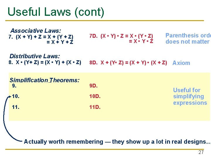
Useful Laws (cont) Associative Laws: 7. (X + Y) + Z = X + (Y + Z) = X + Y + Z 7 D. (X • Y) • Z = X • (Y • Z) = X • Y • Z Parenthesis orde does not matter Distributive Laws: 8. X • (Y+ Z) = (X • Y) + (X • Z) Simplification Theorems: 8 D. X + (Y • Z) = (X + Y) • (X + Z) 9. X • Y + X • = X 9 D. (X + Y) • (X + ) = X 10. X + X • Y = X 10 D. X • (X + Y) = X 11. (X + ) • Y = X • Y 11 D. (X • ) + Y = X + Y Axiom Useful for simplifying expressions Actually worth remembering — they show up a lot in real designs… 27
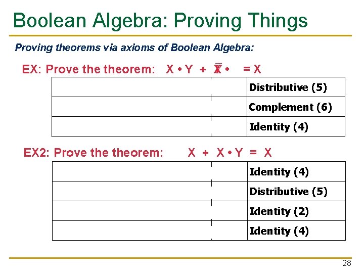
Boolean Algebra: Proving Things Proving theorems via axioms of Boolean Algebra: EX: Prove theorem: X • Y + X • = X X • ( Y + ) = X X • 1 =X X =X Distributive (5) Complement (6) Identity (4) EX 2: Prove theorem: X + X • Y = X X • 1+X • Y =X X • (1+Y) =X Identity (4) Distributive (5) X • 1 =X Identity (2) X =X Identity (4) 28
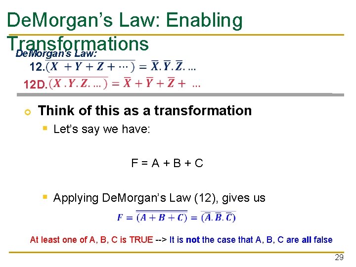
De. Morgan’s Law: Enabling Transformations De. Morgan's Law: 12. 12 D. Think of this as a transformation § Let’s say we have: ¢ F = A + B + C § Applying De. Morgan’s Law (12), gives us At least one of A, B, C is TRUE --> It is not the case that A, B, C are all false 29
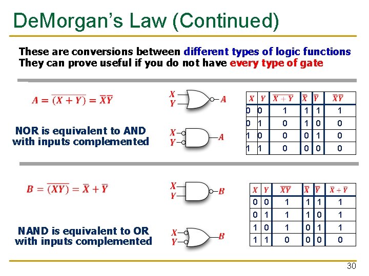
De. Morgan’s Law (Continued) These are conversions between different types of logic functions They can prove useful if you do not have every type of gate NOR is equivalent to AND with inputs complemented NAND is equivalent to OR with inputs complemented 0 0 1 1 0 1 0 1 1 0 0 0 1 1 1 0 1 0 1 1 0 0 30
Using Boolean Equations to Represent a Logic Circuit 31
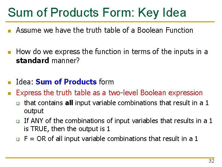
Sum of Products Form: Key Idea n n Assume we have the truth table of a Boolean Function How do we express the function in terms of the inputs in a standard manner? Idea: Sum of Products form Express the truth table as a two-level Boolean expression q q q that contains all input variable combinations that result in a 1 output If ANY of the combinations of input variables that results in a 1 is TRUE, then the output is 1 F = OR of all input variable combinations that result in a 1 32
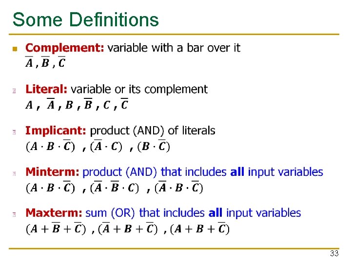
Some Definitions n 33
Two-Level Canonical (Standard) Forms n Truth table is the unique signature of a Boolean function … q n A Boolean function can have many alternative Boolean expressions q n But, it is an expensive representation i. e. , many alternative Boolean expressions (and gate realizations) may have the same truth table (and function) Canonical form: standard form for a Boolean expression q q Provides a unique algebraic signature If they all say the same thing, why do we care? n Different Boolean expressions lead to different gate realizations 34
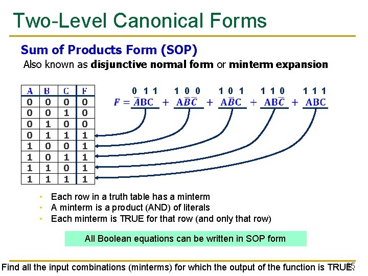
Two-Level Canonical Forms Sum of Products Form (SOP) Also known as disjunctive normal form or minterm expansion 0 0 1 1 0 1 0 1 0 0 0 1 1 1 0 0 1 0 1 1 1 0 1 1 1 • Each row in a truth table has a minterm • A minterm is a product (AND) of literals • Each minterm is TRUE for that row (and only that row) All Boolean equations can be written in SOP form 35 Find all the input combinations (minterms) for which the output of the function is TRUE.
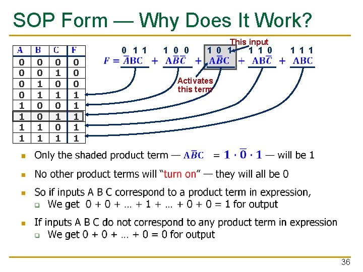
SOP Form — Why Does It Work? 0 0 1 1 0 1 0 1 0 1 1 0 0 0 1 1 1 0 0 This input 1 0 1 1 1 0 1 1 1 Activates this term 36
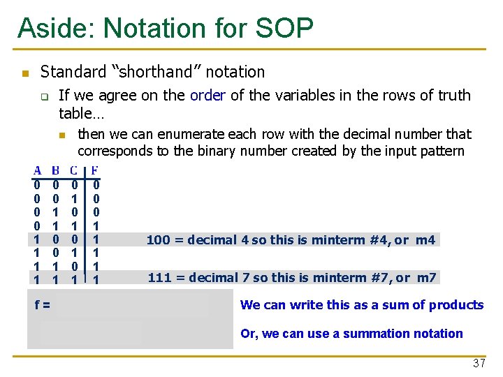
Aside: Notation for SOP Standard “shorthand” notation n q If we agree on the order of the variables in the rows of truth table… n 0 0 1 1 then we can enumerate each row with the decimal number that corresponds to the binary number created by the input pattern 0 0 1 0 0 0 1 1 1 0 1 100 = decimal 4 so this is minterm #4, or m 4 111 = decimal 7 so this is minterm #7, or m 7 f = m 3 + m 4 + m 5 + m 6 + m 7 = ∑m(3, 4, 5, 6, 7) We can write this as a sum of products Or, we can use a summation notation 37

Canonical SOP Forms 0 0 1 1 0 1 0 1 minterms = m 0 = m 1 = m 2 = m 3 = m 4 = m 5 = m 6 = m 7 Shorthand Notation for Minterms of 3 Variables F in canonical form: F(A, B, C) = ∑m(3, 4, 5, 6, 7) = m 3 + m 4 + m 5 + m 6 + m 7 canonical form ≠ minimal form 2 -Level AND/OR Realization 38
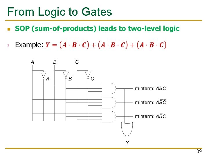
From Logic to Gates n 39
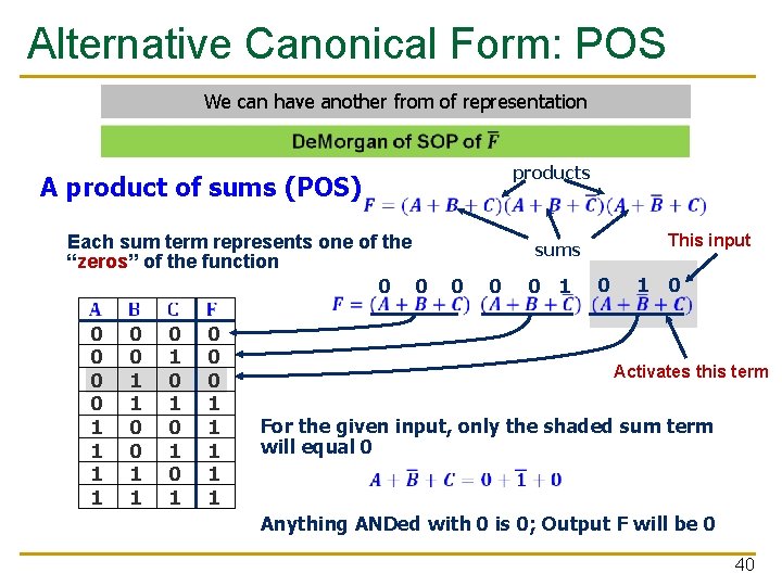
Alternative Canonical Form: POS We can have another from of representation A product of sums (POS) products This input Each sum term represents one of the sums “zeros” of the function 0 0 0 1 0 Activates this term 0 1 0 0 0 1 1 1 For the given input, only the shaded sum term 1 0 0 1 will equal 0 1 1 1 1 0 1 1 1 Anything ANDed with 0 is 0; Output F will be 0 40
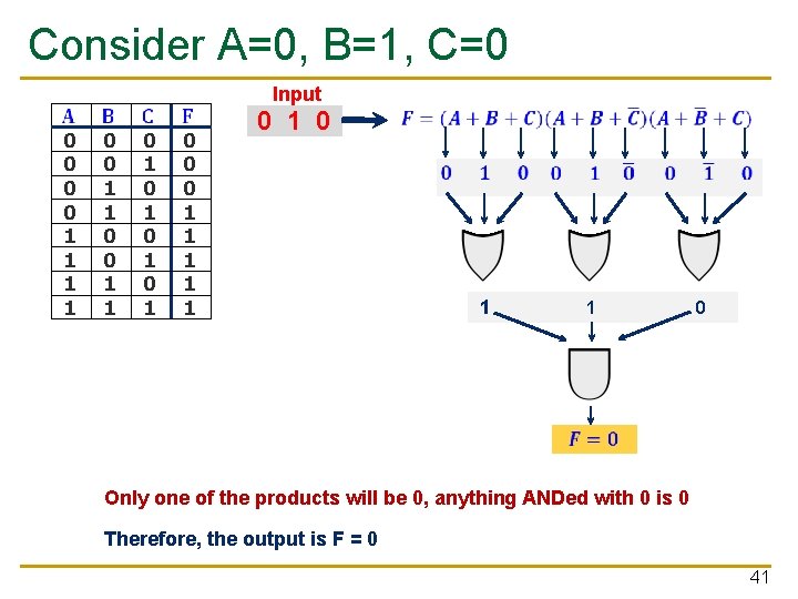
Consider A=0, B=1, C=0 0 0 1 1 0 1 0 1 0 0 0 1 1 1 Input 0 1 0 1 1 0 Only one of the products will be 0, anything ANDed with 0 is 0 Therefore, the output is F = 0 41
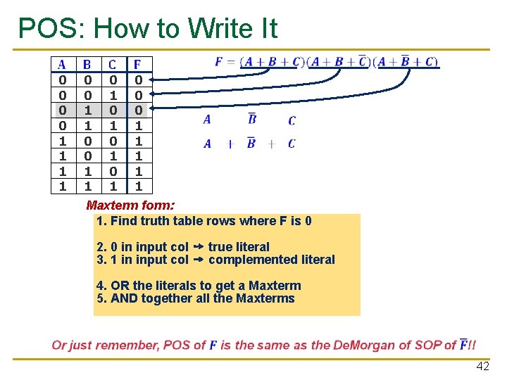
POS: How to Write It 0 0 1 1 0 0 1 1 1 0 0 1 1 1 0 1 1 Maxterm form: 1. Find truth table rows where F is 0 2. 0 in input col ➙ true literal 3. 1 in input col ➙ complemented literal 4. OR the literals to get a Maxterm 5. AND together all the Maxterms 42
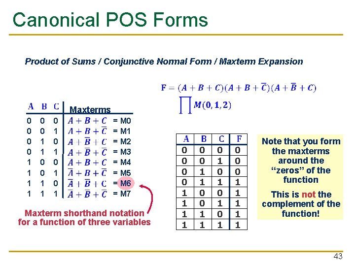
Canonical POS Forms Product of Sums / Conjunctive Normal Form / Maxterm Expansion 0 0 1 1 0 1 0 1 Maxterms = M 0 = M 1 = M 2 = M 3 = M 4 = M 5 = M 6 = M 7 Maxterm shorthand notation for a function of three variables 0 0 1 1 0 1 0 1 0 0 0 1 1 1 Note that you form the maxterms around the “zeros” of the function This is not the complement of the function! 43
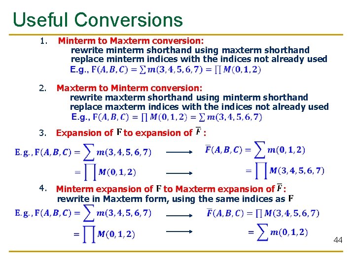
Useful Conversions 1. Minterm to Maxterm conversion: rewrite minterm shorthand using maxterm shorthand replace minterm indices with the indices not already used 2. Maxterm to Minterm conversion: rewrite maxterm shorthand using minterm shorthand replace maxterm indices with the indices not already used 3. Expansion of to expansion of : 4. Minterm expansion of to Maxterm expansion of : rewrite in Maxterm form, using the same indices as 44

Combinational Building Blocks used in Modern Computers 45
Combinational Building Blocks n n n Combinational logic is often grouped into larger building blocks to build more complex systems Hides the unnecessary gate-level details to emphasize the function of the building block We now look at: q q Decoders Multiplexers Full adder PLA (Programmable Logic Array)
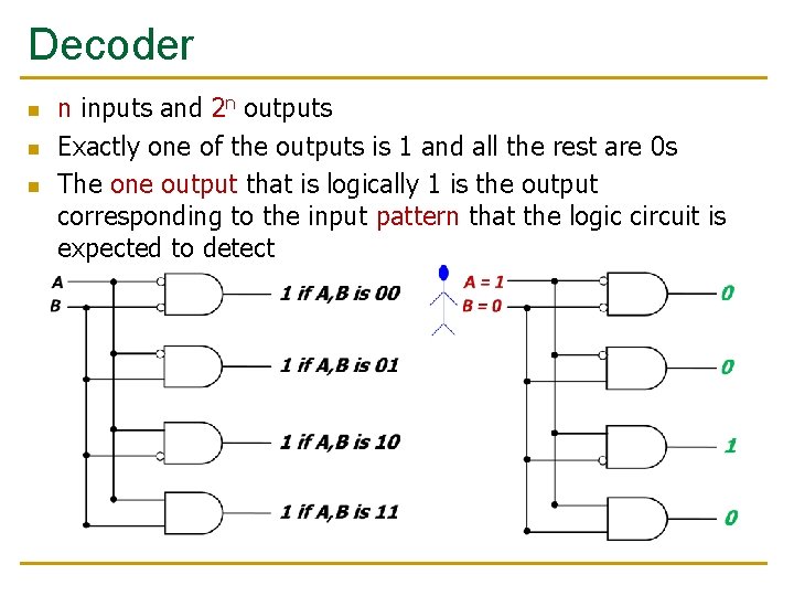
Decoder n n inputs and 2 n outputs Exactly one of the outputs is 1 and all the rest are 0 s The one output that is logically 1 is the output corresponding to the input pattern that the logic circuit is expected to detect
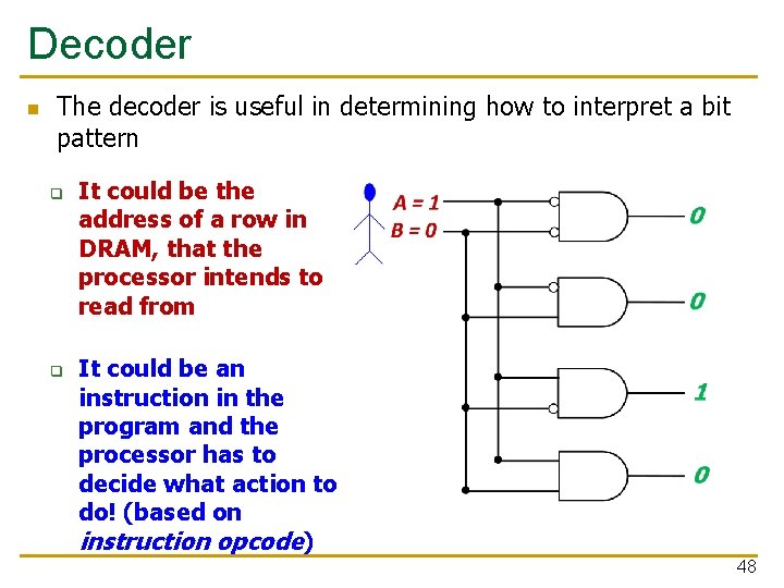
Decoder n The decoder is useful in determining how to interpret a bit pattern q q It could be the address of a row in DRAM, that the processor intends to read from It could be an instruction in the program and the processor has to decide what action to do! (based on instruction opcode) 48
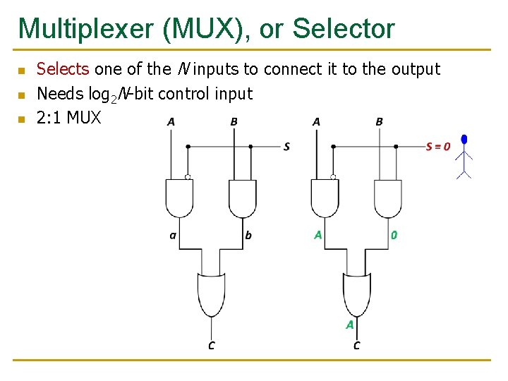
Multiplexer (MUX), or Selector n n n Selects one of the N inputs to connect it to the output Needs log 2 N-bit control input 2: 1 MUX
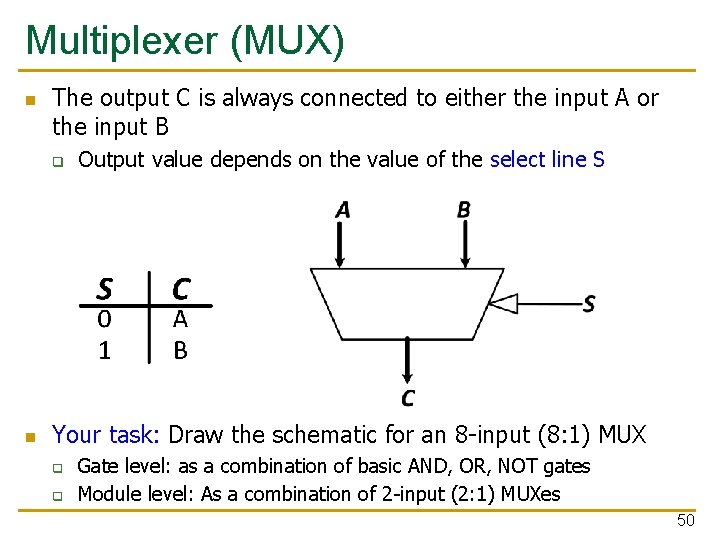
Multiplexer (MUX) n The output C is always connected to either the input A or the input B q n Output value depends on the value of the select line S Your task: Draw the schematic for an 8 -input (8: 1) MUX q q Gate level: as a combination of basic AND, OR, NOT gates Module level: As a combination of 2 -input (2: 1) MUXes 50
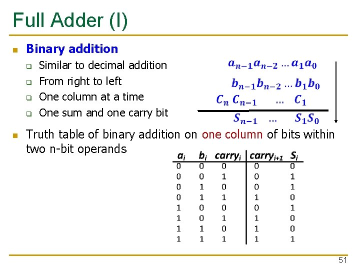
Full Adder (I) n Binary addition q q n Similar to decimal addition From right to left One column at a time One sum and one carry bit Truth table of binary addition on one column of bits within two n-bit operands 51
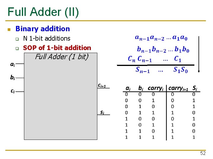
Full Adder (II) n Binary addition q q N 1 -bit additions SOP of 1 -bit addition Full Adder (1 bit) 52
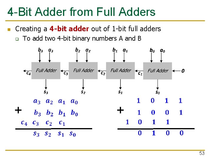
4 -Bit Adder from Full Adders n Creating a 4 -bit adder out of 1 -bit full adders To add two 4 -bit binary numbers A and B q + + 53
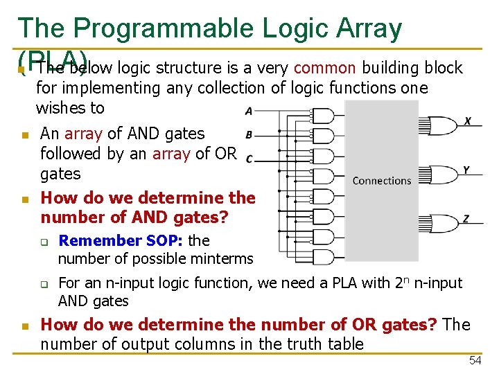
The Programmable Logic Array (PLA) n The below logic structure is a very common building block for implementing any collection of logic functions one wishes to n n An array of AND gates followed by an array of OR gates How do we determine the number of AND gates? q q n Remember SOP: the number of possible minterms For an n-input logic function, we need a PLA with 2 n n-input AND gates How do we determine the number of OR gates? The number of output columns in the truth table 54
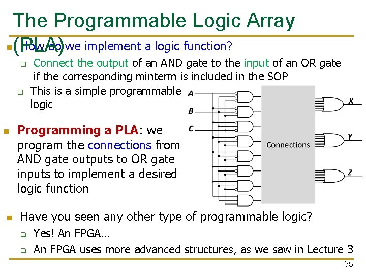
The Programmable Logic Array n(PLA) How do we implement a logic function? q q n n Connect the output of an AND gate to the input of an OR gate if the corresponding minterm is included in the SOP This is a simple programmable logic Programming a PLA: we program the connections from AND gate outputs to OR gate inputs to implement a desired logic function Have you seen any other type of programmable logic? q q Yes! An FPGA… An FPGA uses more advanced structures, as we saw in Lecture 3 55
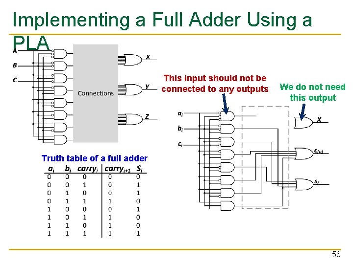
Implementing a Full Adder Using a PLA This input should not be connected to any outputs We do not need this output Truth table of a full adder 56
Logical (Functional) Completeness n Any logic function we wish to implement could be accomplished with a PLA q q n n PLA consists of only AND gates, OR gates, and inverters We just have to program connections based on SOP of the intended logic function The set of gates {AND, OR, NOT} is logically complete because we can build a circuit to carry out the specification of any truth table we wish, without using any other kind of gate NAND is also logically complete. So is NOR. q Your task: Prove this. 57
More Combinational Building Blocks n H&H Chapter 2 in full q q n H&H Chapter 5 q n Required Reading E. g. , see Tri-state Buffer and Z values in Section 2. 6 Will be required reading soon. You will benefit greatly by reading the “combinational” parts of Chapter 5 soon. q Sections 5. 1 and 5. 2 58
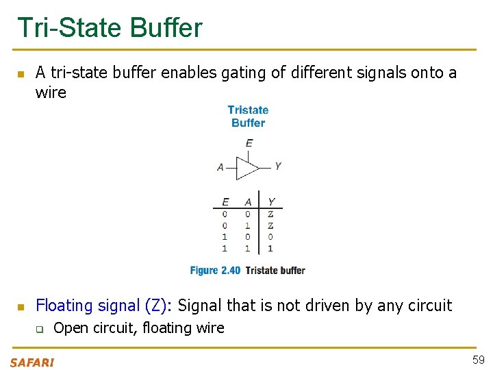
Tri-State Buffer n n A tri-state buffer enables gating of different signals onto a wire Floating signal (Z): Signal that is not driven by any circuit q Open circuit, floating wire 59

Example: Use of Tri-State Buffers n Imagine a wire connecting the CPU and memory q q At any time only the CPU or the memory can place a value on the wire, both not both You can have two tri-state buffers: one driven by CPU, the other memory; and ensure at most one is enabled at any time 60
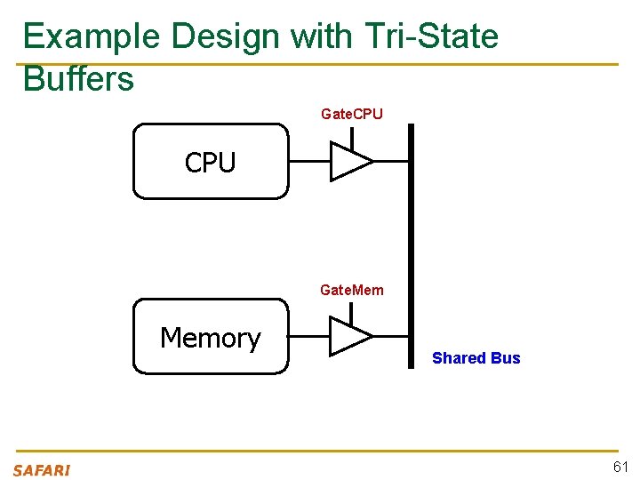
Example Design with Tri-State Buffers Gate. CPU Gate. Memory Shared Bus 61
Logic Simplification: Karnaugh Maps (KMaps) 62
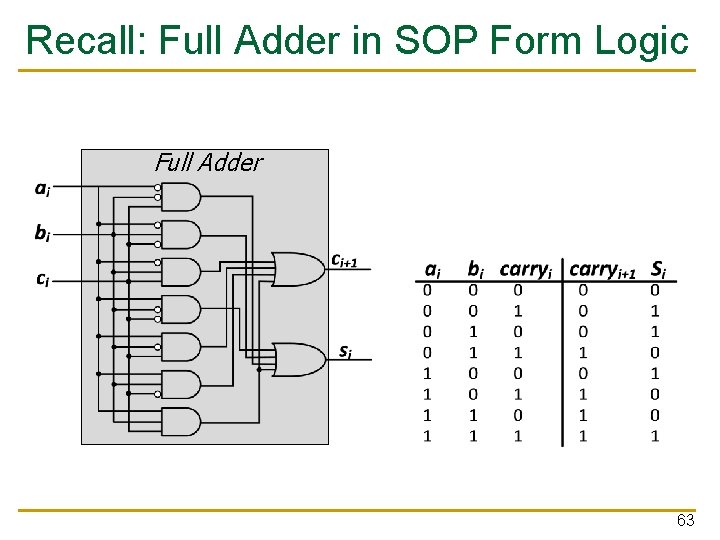
Recall: Full Adder in SOP Form Logic Full Adder 63
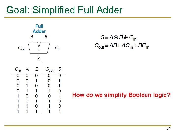
Goal: Simplified Full Adder How do we simplify Boolean logic? 64
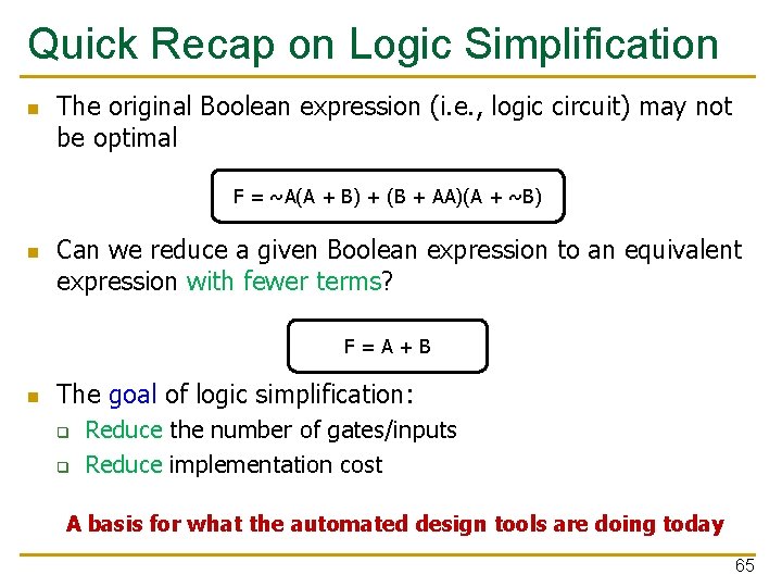
Quick Recap on Logic Simplification n The original Boolean expression (i. e. , logic circuit) may not be optimal F = ~A(A + B) + (B + AA)(A + ~B) n Can we reduce a given Boolean expression to an equivalent expression with fewer terms? F = A + B n The goal of logic simplification: q q Reduce the number of gates/inputs Reduce implementation cost A basis for what the automated design tools are doing today 65
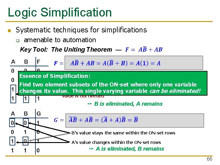
Logic Simplification n Systematic techniques for simplifications q amenable to automation Key Tool: The Uniting Theorem — B's value changes within the rows where F==1 (“ON set”) Essence of Simplification: A's subsets value doesof NOT change within the ON-set Find two element the ON-set where onlyrows one variable If an. This inputsingle (B) can varying change without changing that input changes its value. variable canthe beoutput, eliminated! value is not needed ➙ B is eliminated, A remains B's value stays the same within the ON-set rows A's value changes within the ON-set rows ➙ A is eliminated, B remains 66
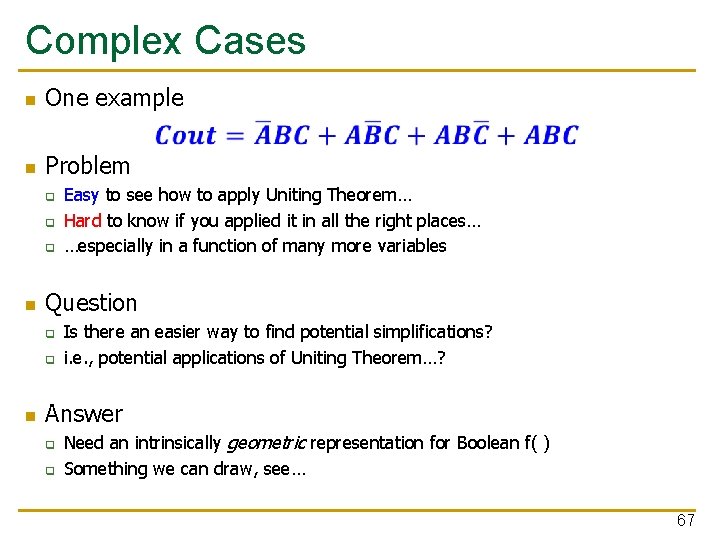
Complex Cases One example n Problem n q q q n Question q q n Easy to see how to apply Uniting Theorem… Hard to know if you applied it in all the right places… …especially in a function of many more variables Is there an easier way to find potential simplifications? i. e. , potential applications of Uniting Theorem…? Answer q q Need an intrinsically geometric representation for Boolean f( ) Something we can draw, see… 67
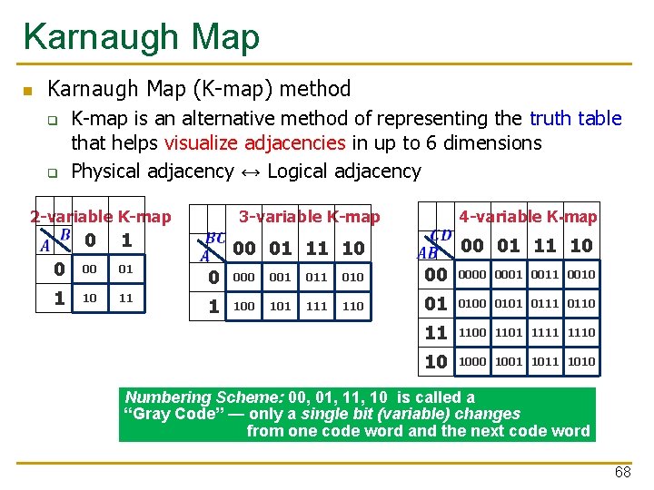
Karnaugh Map n Karnaugh Map (K-map) method q q K-map is an alternative method of representing the truth table that helps visualize adjacencies in up to 6 dimensions Physical adjacency ↔ Logical adjacency 2 -variable K-map 0 1 0 00 01 1 10 11 4 -variable K-map 3 -variable K-map 00 01 11 10 0 001 010 00 0001 0010 1 100 101 110 01 0100 0101 0110 11 1100 1101 1110 10 1001 1010 Numbering Scheme: 00, 01, 10 is called a “Gray Code” — only a single bit (variable) changes from one code word and the next code word 68
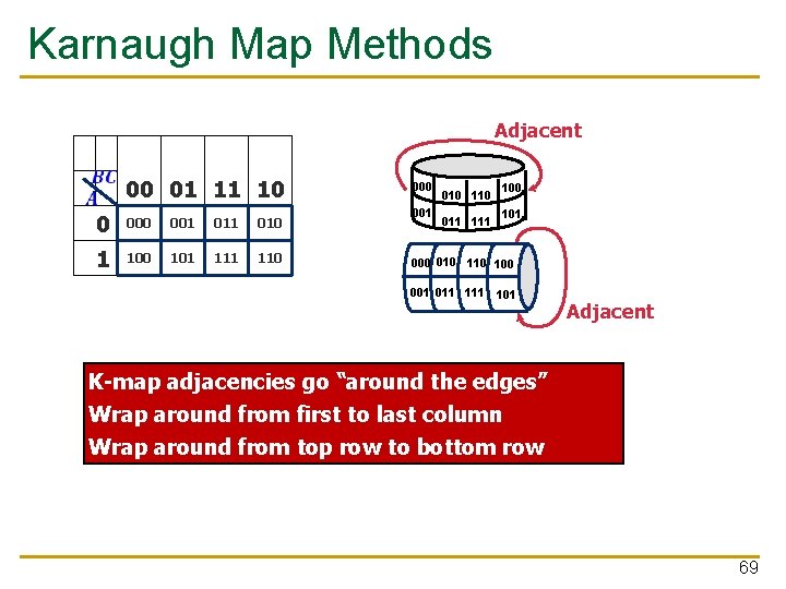
Karnaugh Map Methods Adjacent 00 01 11 10 0 001 010 1 100 101 110 001 010 110 011 100 101 000 010 100 001 011 101 Adjacent K-map adjacencies go “around the edges” Wrap around from first to last column Wrap around from top row to bottom row 69
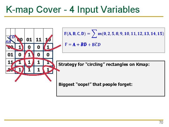
K-map Cover - 4 Input Variables 00 01 11 10 00 1 01 0 0 11 1 1 10 1 1 Strategy for “circling” rectangles on Kmap: As big as possible Biggest “oops!” that people forget: Wrap-arounds 70
Logic Minimization Using K-Maps n Very simple guideline: q Circle all the rectangular blocks of 1’s in the map, using the fewest possible number of circles n q n Each circle should be as large as possible Read off the implicants that were circled More formally: q q q A Boolean equation is minimized when it is written as a sum of the fewest number of prime implicants Each circle on the K-map represents an implicant The largest possible circles are prime implicants 72
K-map Rules n 73
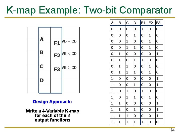
K-map Example: Two-bit Comparator A B C F 1 AB = CD F 2 AB < CD F 3 AB > CD D Design Approach: Write a 4 -Variable K-map for each of the 3 output functions A B C D F 1 F 2 F 3 0 0 0 0 1 0 1 0 0 0 1 1 0 0 1 0 1 1 0 0 1 1 1 0 1 0 0 0 1 1 0 1 0 1 1 0 0 1 1 0 0 0 1 1 1 0 0 74
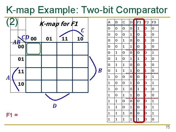
K-map Example: Two-bit Comparator (2) K-map for F 1 00 01 11 10 1 F 1 = A'B'C'D' + A'BC'D + ABCD + AB'CD' A B C D F 1 F 2 F 3 0 0 0 0 1 0 1 0 0 0 1 1 0 0 1 0 1 1 0 0 1 1 1 0 1 0 0 0 1 1 0 1 0 1 1 0 0 1 1 0 0 0 1 1 1 0 0 75
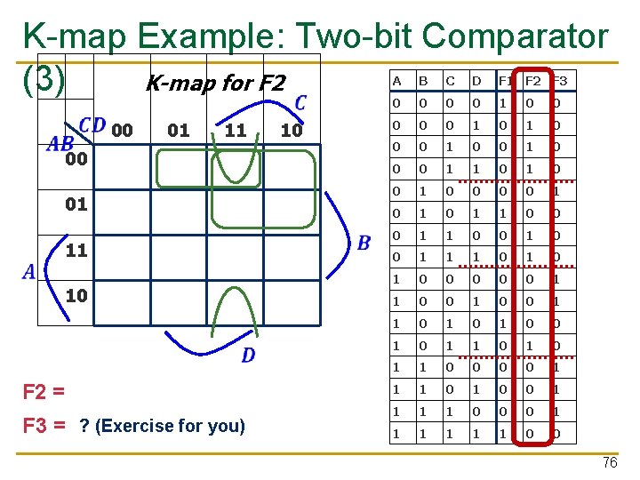
K-map Example: Two-bit Comparator K-map for F 2 (3) A B C D F 1 F 2 F 3 0 0 1 0 0 01 11 10 0 1 0 1 1 1 0 0 1 0 0 1 0 1 1 0 0 1 1 1 0 1 0 0 0 1 1 1 0 0 1 1 0 1 0 1 1 0 0 1 F 2 = A'C + A'B'D + B'CD 1 1 0 0 0 1 1 1 0 0 00 01 00 1 11 10 1 F 3 = ? (Exercise for you) 76

Design of Digital Circuits Lecture 5: Combinational Logic II Prof. Onur Mutlu ETH Zurich Spring 2019 7 March 2019

We did not cover the remaining slides. They are for your preparation for the next lecture. 78
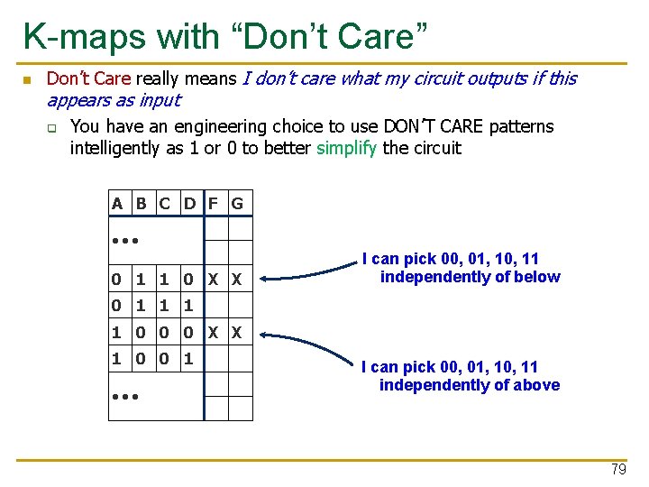
K-maps with “Don’t Care” n Don’t Care really means I don’t care what my circuit outputs if this appears as input q You have an engineering choice to use DON’T CARE patterns intelligently as 1 or 0 to better simplify the circuit A B C D F G • • • 0 1 1 0 X X I can pick 00, 01, 10, 11 independently of below 0 1 1 0 0 0 X X 1 0 0 1 • • • I can pick 00, 01, 10, 11 independently of above 79
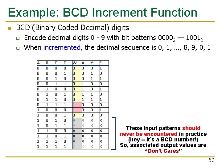
Example: BCD Increment Function n BCD (Binary Coded Decimal) digits q q Encode decimal digits 0 - 9 with bit patterns 00002 — 10012 When incremented, the decimal sequence is 0, 1, …, 8, 9, 0, 1 A 0 0 0 0 1 1 1 1 B 0 0 0 0 1 1 1 1 C 0 0 1 1 D 0 1 0 1 W 0 0 0 0 1 1 0 X X X X 0 0 0 1 1 0 0 0 X X X Y 0 1 1 0 0 0 X X X Z 1 0 1 0 1 0 X X X These input patterns should never be encountered in practice (hey -- it’s a BCD number!) So, associated output values are “Don’t Cares” 80
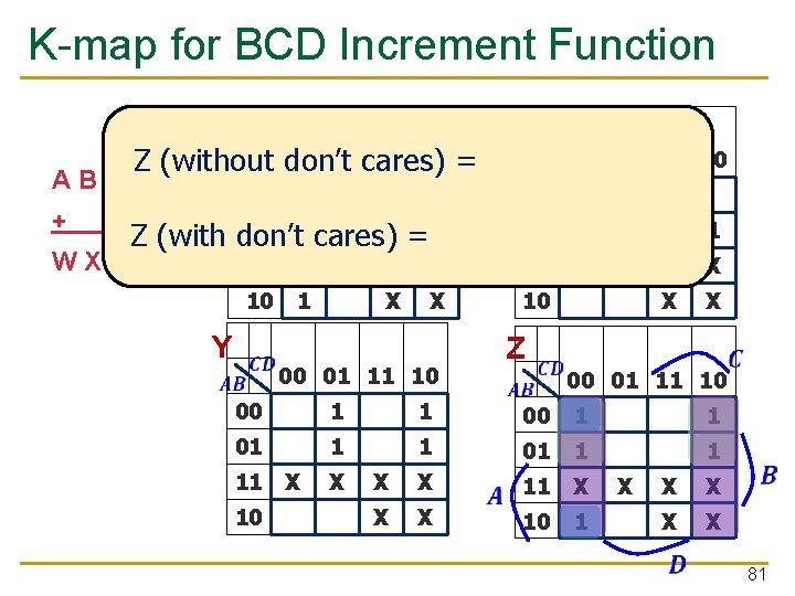
K-map for BCD Increment Function W X 00 01 11 10 00 B'C'D’ 01 11 Z (without don’t cares) = A'D' + A B C D 00 + 1 00 01 1 Z (with don’t cares) = D' W X Y Z Y 11 X 10 01 1 10 X X 1 X 1 11 00 11 1 X Z 00 01 11 10 1 01 X 10 1 X X 00 01 11 10 00 1 1 1 01 1 1 X X 11 X X X 10 1 X X X 81
K-map Summary n Karnaugh maps as a formal systematic approach for logic simplification n 2 -, 3 -, 4 -variable K-maps n K-maps with “Don’t Care” outputs n H&H Section 2. 7 82
Hardware Description Languages & Verilog (Combinational Logic) 83
Agenda n Implementing Combinational Logic q q q Hardware Description Languages Hardware Design Methodologies Verilog 84
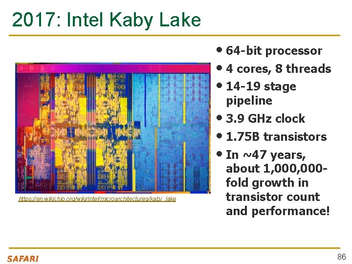
2017: Intel Kaby Lake • 64 -bit processor • 4 cores, 8 threads • 14 -19 stage pipeline • 3. 9 GHz clock • 1. 75 B transistors • In ~47 years, https: //en. wikichip. org/wiki/intel/microarchitectures/kaby_lake about 1, 000 fold growth in transistor count and performance! 86
How to Deal with This Complexity? n Hardware Description Languages! n A fact of life in computer engineering q Need to be able to specify complex designs n q q … and to simulate their behavior n yes, it’s what I want to build … and to synthesize (automatically design) portions of it n n communicate with others in your design group have an error-free path to implementation Hardware Description Languages q Many similarly featured HDLs (e. g. , Verilog, VHDL, . . . ) n n if you learn one, it is not hard to learn another mapping between languages is typically mechanical, especially for the commonly used subset 87

Hardware Description Languages n Two well-known hardware description languages n Verilog q q q n VHDL (VHSIC Hardware Description Language) q q q n Developed in 1984 by Gateway Design Automation Became an IEEE standard (1364) in 1995 More popular in US Developed in 1981 by the Department of Defense Became an IEEE standard (1076) in 1987 More popular in Europe In this course we will use Verilog 88

Hardware Design Using Verilog 89
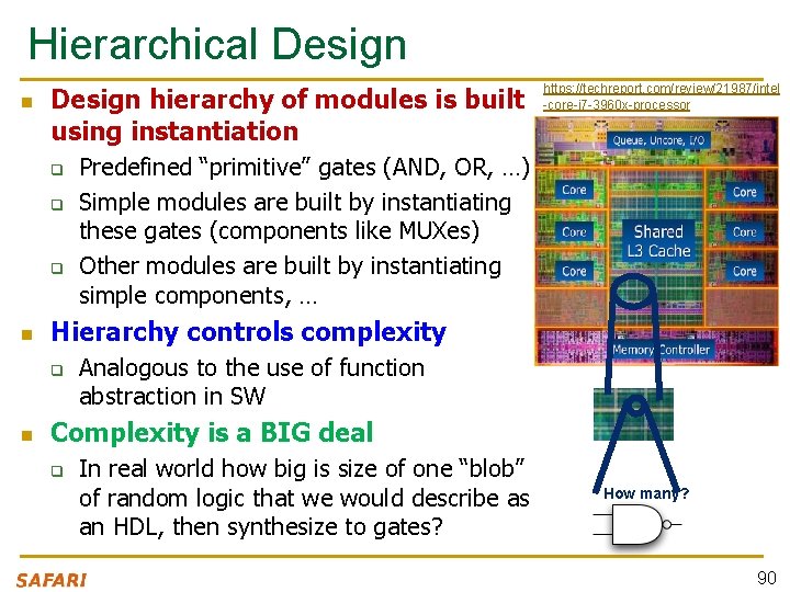
Hierarchical Design n Design hierarchy of modules is built using instantiation q q q n Predefined “primitive” gates (AND, OR, …) Simple modules are built by instantiating these gates (components like MUXes) Other modules are built by instantiating simple components, … Hierarchy controls complexity q n https: //techreport. com/review/21987/intel -core-i 7 -3960 x-processor Analogous to the use of function abstraction in SW Complexity is a BIG deal q In real world how big is size of one “blob” of random logic that we would describe as an HDL, then synthesize to gates? How many? 90
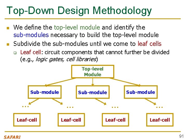
Top-Down Design Methodology n n We define the top-level module and identify the sub-modules necessary to build the top-level module Subdivide the sub-modules until we come to leaf cells q Leaf cell: circuit components that cannot further be divided (e. g. , logic gates, cell libraries) Top-level Module Sub-module … … Leaf-cell 91
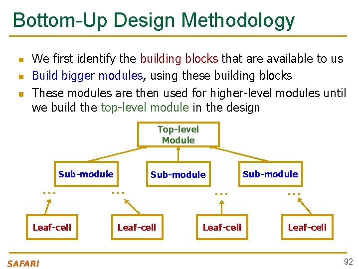
Bottom-Up Design Methodology n n n We first identify the building blocks that are available to us Build bigger modules, using these building blocks These modules are then used for higher-level modules until we build the top-level module in the design Top-level Module … Sub-module Leaf-cell Sub-module … Leaf-cell 92
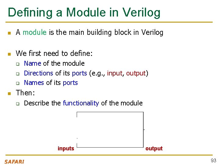
Defining a Module in Verilog n A module is the main building block in Verilog n We first need to define: q q q n Name of the module Directions of its ports (e. g. , input, output) Names of its ports Then: q Describe the functionality of the module example inputs output 93
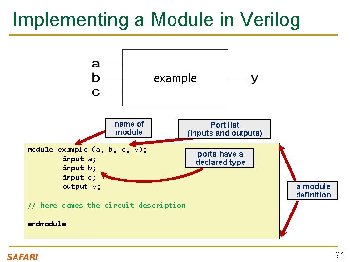
Implementing a Module in Verilog example name of module example (a, b, c, y); input a; input b; input c; output y; Port list (inputs and outputs) ports have a declared type a module definition // here comes the circuit description endmodule 94
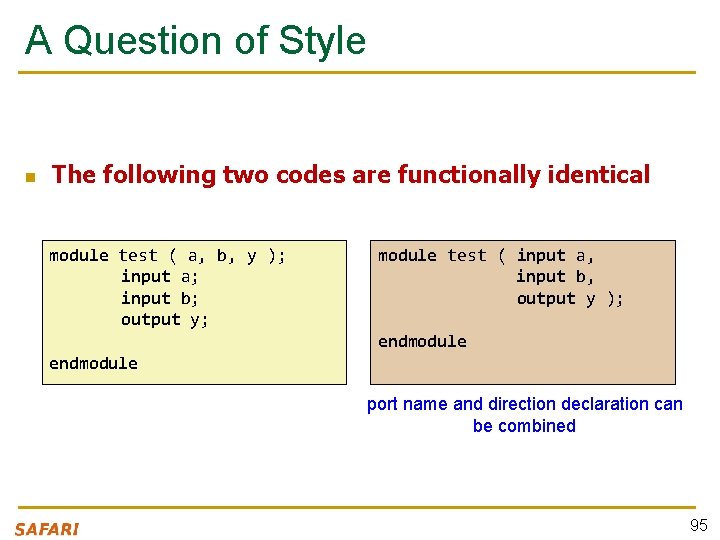
A Question of Style n The following two codes are functionally identical module test ( a, b, y ); input a; input b; output y; module test ( input a, input b, output y ); endmodule port name and direction declaration can be combined 95
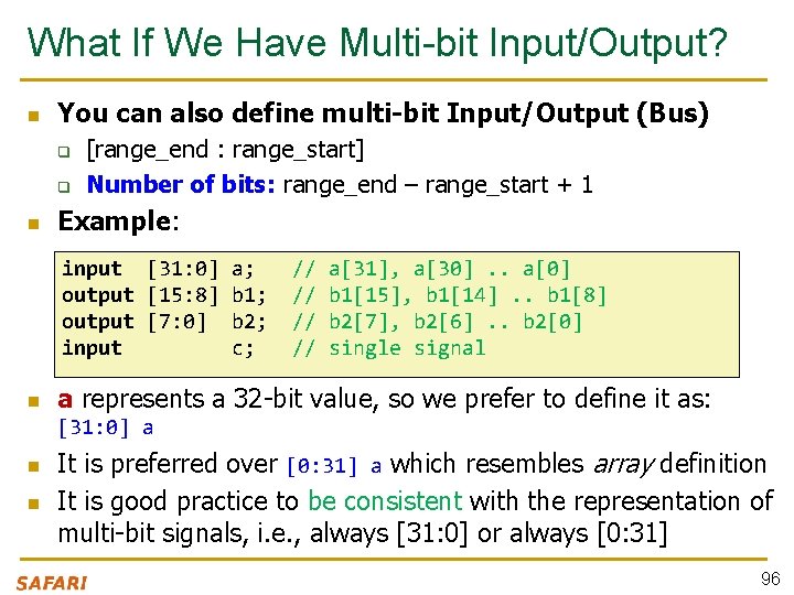
What If We Have Multi-bit Input/Output? n You can also define multi-bit Input/Output (Bus) q q n [range_end : range_start] Number of bits: range_end – range_start + 1 Example: input [31: 0] a; output [15: 8] b 1; output [7: 0] b 2; input c; n // // a[31], a[30]. . a[0] b 1[15], b 1[14]. . b 1[8] b 2[7], b 2[6]. . b 2[0] single signal a represents a 32 -bit value, so we prefer to define it as: [31: 0] a n n It is preferred over [0: 31] a which resembles array definition It is good practice to be consistent with the representation of multi-bit signals, i. e. , always [31: 0] or always [0: 31] 96
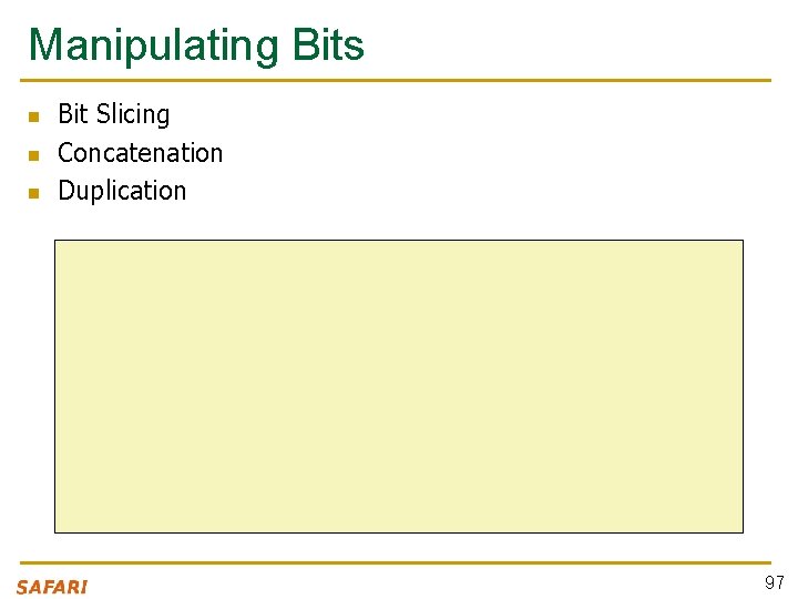
Manipulating Bits n n n Bit Slicing Concatenation Duplication // You can assign partial buses wire [15: 0] longbus; wire [7: 0] shortbus; assign shortbus = longbus[12: 5]; // Concatenating is by {} assign y = {a[2], a[1], a[0]}; // Possible to define multiple copies assign x = {a[0], a[0]} assign y = { 4{a[0]} } 97
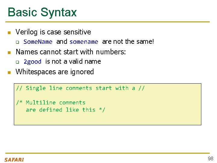
Basic Syntax n Verilog is case sensitive q n Names cannot start with numbers: q n Some. Name and somename are not the same! 2 good is not a valid name Whitespaces are ignored // Single line comments start with a // /* Multiline comments are defined like this */ 98
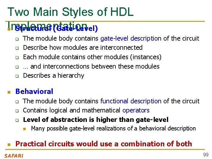
Two Main Styles of HDL Implementation n Structural (Gate-Level) q q q n The module body contains gate-level description of the circuit Describe how modules are interconnected Each module contains other modules (instances) … and interconnections between these modules Describes a hierarchy Behavioral q q q The module body contains functional description of the circuit Contains logical and mathematical operators Level of abstraction is higher than gate-level n n Many possible gate-level realizations of a behavioral description Practical circuits would use a combination of both 99
Structural (Gate-Level) HDL 100
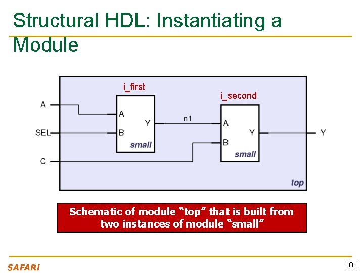
Structural HDL: Instantiating a Module i_first i_second Schematic of module “top” that is built from two instances of module “small” 101
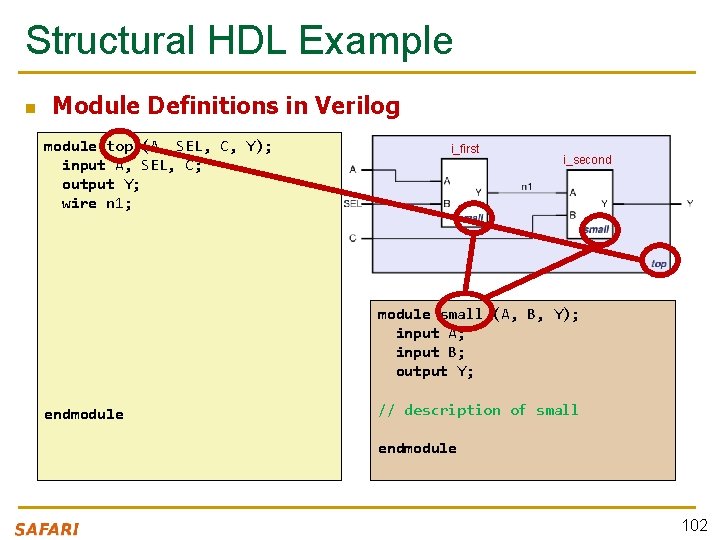
Structural HDL Example n Module Definitions in Verilog module top (A, SEL, C, Y); input A, SEL, C; output Y; wire n 1; i_first i_second module small (A, B, Y); input A; input B; output Y; endmodule // description of small endmodule 102
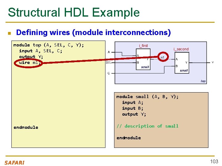
Structural HDL Example n Defining wires (module interconnections) module top (A, SEL, C, Y); input A, SEL, C; output Y; wire n 1; i_first i_second module small (A, B, Y); input A; input B; output Y; endmodule // description of small endmodule 103
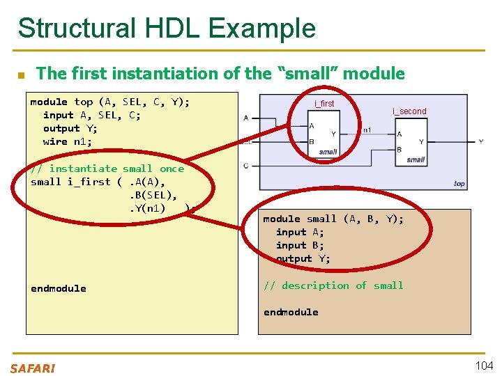
Structural HDL Example n The first instantiation of the “small” module top (A, SEL, C, Y); input A, SEL, C; output Y; wire n 1; // instantiate small once small i_first (. A(A), . B(SEL), . Y(n 1) ); endmodule i_first i_second module small (A, B, Y); input A; input B; output Y; // description of small endmodule 104
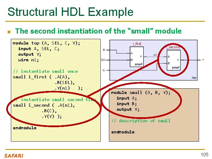
Structural HDL Example n The second instantiation of the “small” module top (A, SEL, C, Y); input A, SEL, C; output Y; wire n 1; // instantiate small once small i_first (. A(A), . B(SEL), . Y(n 1) ); // instantiate small second time small i_second (. A(n 1), . B(C), . Y(Y) ); endmodule i_first i_second module small (A, B, Y); input A; input B; output Y; // description of small endmodule 105
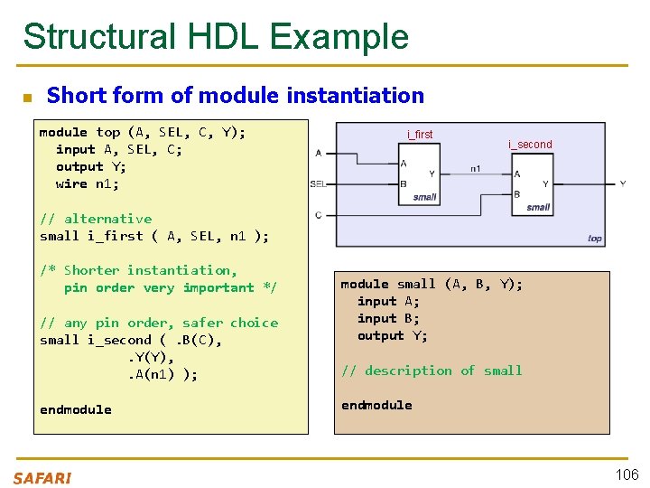
Structural HDL Example n Short form of module instantiation module top (A, SEL, C, Y); input A, SEL, C; output Y; wire n 1; i_first i_second // alternative small i_first ( A, SEL, n 1 ); /* Shorter instantiation, pin order very important */ // any pin order, safer choice small i_second (. B(C), . Y(Y), . A(n 1) ); endmodule small (A, B, Y); input A; input B; output Y; // description of small endmodule 106
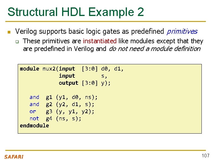
Structural HDL Example 2 n Verilog supports basic logic gates as predefined primitives q These primitives are instantiated like modules except that they are predefined in Verilog and do not need a module definition module mux 2(input [3: 0] d 0, d 1, input s, output [3: 0] y); and g 1 and g 2 or g 3 not g 4 endmodule (y 1, d 0, ns); (y 2, d 1, s); (y, y 1, y 2); (ns, s); 107

Behavioral HDL 108
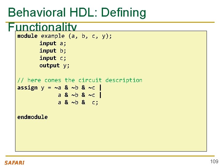
Behavioral HDL: Defining Functionality module example (a, b, c, y); input a; input b; input c; output y; // here comes assign y = ~a a a the circuit description & ~b & ~c | & ~b & c; endmodule 109
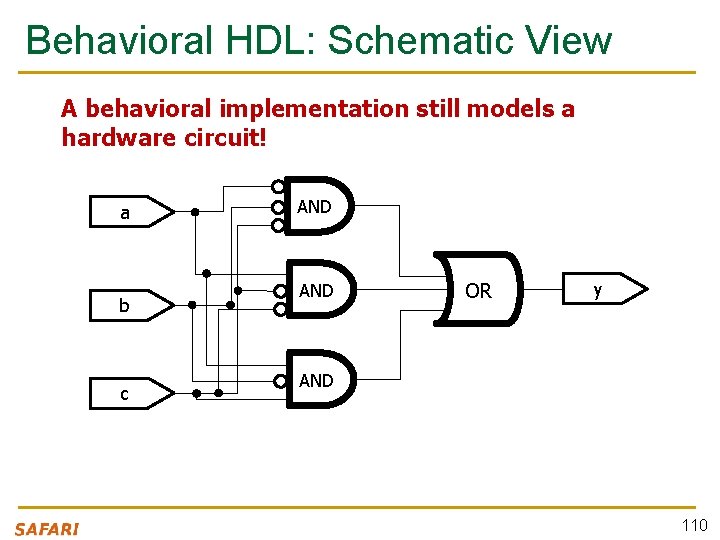
Behavioral HDL: Schematic View A behavioral implementation still models a hardware circuit! a b c AND OR y AND 110
![Bitwise Operators in Behavioral Verilog module gates(input [3: 0] a, b, output [3: 0] Bitwise Operators in Behavioral Verilog module gates(input [3: 0] a, b, output [3: 0]](http://slidetodoc.com/presentation_image_h/2296460e6ab8856836ef54b82a439269/image-109.jpg)
Bitwise Operators in Behavioral Verilog module gates(input [3: 0] a, b, output [3: 0] y 1, y 2, y 3, y 4, y 5); /* Five different two-input logic gates acting on 4 bit buses */ assign assign y 1 y 2 y 3 y 4 y 5 = = = a & a | a ^ ~(a b; b; b; & b); | b); // // // AND OR XOR NAND NOR endmodule 111
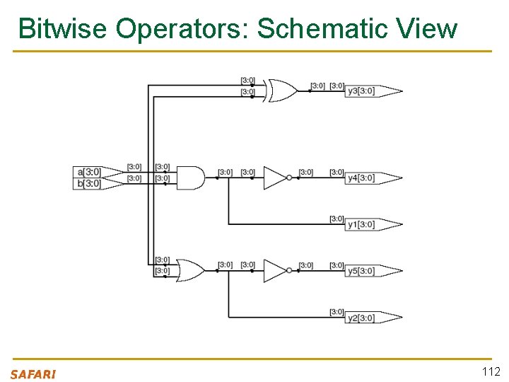
Bitwise Operators: Schematic View 112
![Reduction Operators in Behavioral Verilog module and 8(input [7: 0] a, output y); assign Reduction Operators in Behavioral Verilog module and 8(input [7: 0] a, output y); assign](http://slidetodoc.com/presentation_image_h/2296460e6ab8856836ef54b82a439269/image-111.jpg)
Reduction Operators in Behavioral Verilog module and 8(input [7: 0] a, output y); assign y = &a; // &a is much easier to write than // assign y = a[7] & a[6] & a[5] & a[4] & // a[3] & a[2] & a[1] & a[0]; endmodule 113
![Reduction Operators: Schematic View [0] [1] [2] a[7: 0] [3] [4] AND y [5] Reduction Operators: Schematic View [0] [1] [2] a[7: 0] [3] [4] AND y [5]](http://slidetodoc.com/presentation_image_h/2296460e6ab8856836ef54b82a439269/image-112.jpg)
Reduction Operators: Schematic View [0] [1] [2] a[7: 0] [3] [4] AND y [5] [6] [7] 8 -input AND gate 114
![Conditional Assignment in Behavioral Verilog module mux 2(input [3: 0] d 0, d 1, Conditional Assignment in Behavioral Verilog module mux 2(input [3: 0] d 0, d 1,](http://slidetodoc.com/presentation_image_h/2296460e6ab8856836ef54b82a439269/image-113.jpg)
Conditional Assignment in Behavioral Verilog module mux 2(input [3: 0] d 0, d 1, input s, output [3: 0] y); assign y = s ? d 1 : d 0; // if (s) then y=d 1 else y=d 0; endmodule n ? : is also called a ternary operator as it operates on three inputs: q q q s d 1 d 0 115
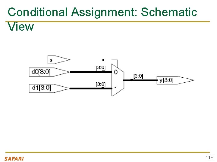
Conditional Assignment: Schematic View 116
![More Complex Conditional Assignments module mux 4(input [3: 0] d 0, d 1, d More Complex Conditional Assignments module mux 4(input [3: 0] d 0, d 1, d](http://slidetodoc.com/presentation_image_h/2296460e6ab8856836ef54b82a439269/image-115.jpg)
More Complex Conditional Assignments module mux 4(input [3: 0] d 0, d 1, d 2, d 3 input [1: 0] s, output [3: 0] y); assign y = s[1] ? ( : ( // if (s 1) then // if (s 0) then // else // if (s 0) then s[0] ? d 3 : d 2) s[0] ? d 1 : d 0); y=d 3 else y=d 2 y=d 1 else y=d 0 endmodule 117
![Even More Complex Conditional Assignments module mux 4(input [3: 0] d 0, d 1, Even More Complex Conditional Assignments module mux 4(input [3: 0] d 0, d 1,](http://slidetodoc.com/presentation_image_h/2296460e6ab8856836ef54b82a439269/image-116.jpg)
Even More Complex Conditional Assignments module mux 4(input [3: 0] d 0, d 1, d 2, d 3 input [1: 0] s, output [3: 0] y); // // assign y = (s == 2’b 11) ? d 3 : (s == 2’b 10) ? d 2 : (s == 2’b 01) ? d 1 : d 0; if (s = “ 11” ) then y= d 3 else if (s = “ 10” ) then y= d 2 else if (s = “ 01” ) then y= d 1 else y= d 0 endmodule 118
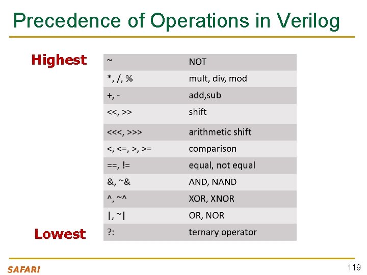
Precedence of Operations in Verilog Highest Lowest 119
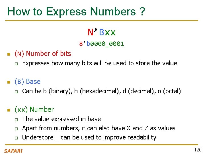
How to Express Numbers ? N’Bxx 8’b 0000_0001 n (N) Number of bits q n (B) Base q n Expresses how many bits will be used to store the value Can be b (binary), h (hexadecimal), d (decimal), o (octal) (xx) Number q q q The value expressed in base Apart from numbers, it can also have X and Z as values Underscore _ can be used to improve readability 120
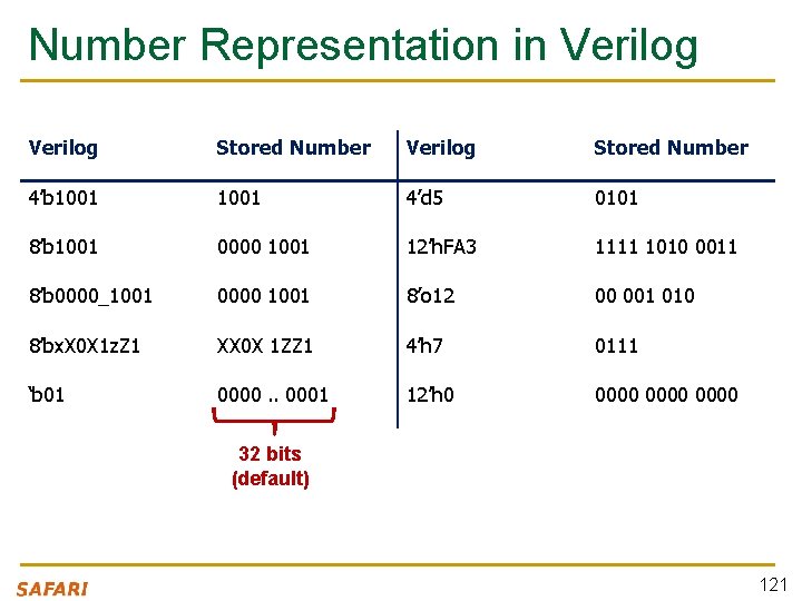
Number Representation in Verilog Stored Number 4’b 1001 4’d 5 0101 8’b 1001 0000 1001 12’h. FA 3 1111 1010 0011 8’b 0000_1001 0000 1001 8’o 12 00 001 010 8’bx. X 0 X 1 z. Z 1 XX 0 X 1 ZZ 1 4’h 7 0111 ‘b 01 0000. . 0001 12’h 0 0000 32 bits (default) 121
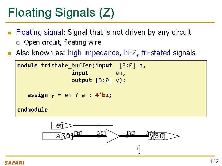
Floating Signals (Z) n Floating signal: Signal that is not driven by any circuit q n Open circuit, floating wire Also known as: high impedance, hi-Z, tri-stated signals module tristate_buffer(input [3: 0] a, input en, output [3: 0] y); assign y = en ? a : 4'bz; endmodule 122
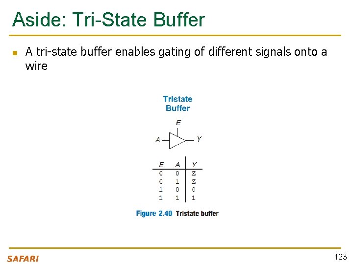
Aside: Tri-State Buffer n A tri-state buffer enables gating of different signals onto a wire 123
Example: Use of Tri-State Buffers n Imagine a wire connecting the CPU and memory q q At any time only the CPU or the memory can place a value on the wire, both not both You can have two tri-state buffers: one driven by CPU, the other memory; and ensure at most one is enabled at any time 124

Example Design with Tri-State Buffers Gate. CPU Gate. Memory Shared Bus 125
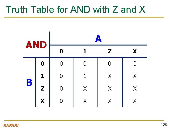
Truth Table for AND with Z and X AND B A 0 1 Z X 0 0 0 1 X X Z 0 X X X 126
What Happens with HDL Code? n Synthesis q q q Modern tools are able to map a HDL code into low-level cell libraries They can perform many optimizations … however they can not guarantee that a solution is optimal n q n Mainly due to computationally expensive placement and routing algorithms Most common way of Digital Design these days Simulation q q Allows the behavior of the circuit to be verified without actually manufacturing the circuit Simulators can work on structural or behavioral HDL 127
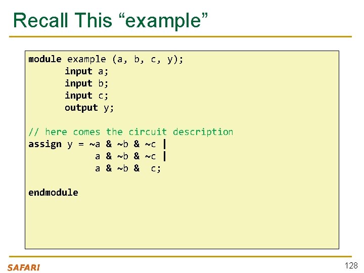
Recall This “example” module example (a, b, c, y); input a; input b; input c; output y; // here comes assign y = ~a a a the circuit description & ~b & ~c | & ~b & c; endmodule 128
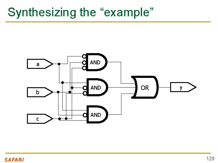
Synthesizing the “example” a b c AND OR y AND 129
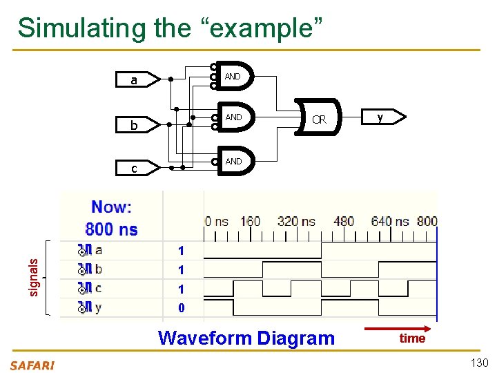
Simulating the “example” AND a AND b OR y AND c signals 1 1 1 0 Waveform Diagram time 130
What We Have Seen So Far n Describing structural hierarchy with Verilog q Instantiate modules in an other module n Describing functionality using behavioral modeling n Writing simple logic equations q n We can write AND, OR, XOR, … Multiplexer functionality q If … then … else n We can describe constants n But there is more. . . 131
More Verilog Examples n n We can write Verilog code in many different ways Let’s see how we can express the same functionality by developing Verilog code q At low-level n n q Poor readability More optimization opportunities At a higher-level of abstraction n n Better readability Limited optimization 132
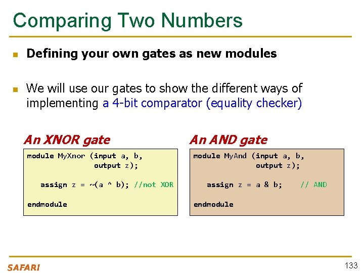
Comparing Two Numbers n n Defining your own gates as new modules We will use our gates to show the different ways of implementing a 4 -bit comparator (equality checker) An XNOR gate module My. Xnor (input a, b, output z); assign z = ~(a ^ b); //not XOR endmodule An AND gate module My. And (input a, b, output z); assign z = a & b; // AND endmodule 133
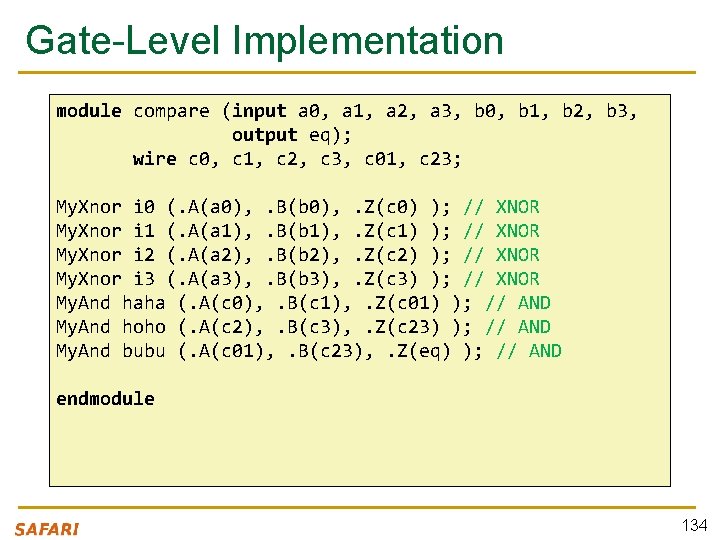
Gate-Level Implementation module compare (input a 0, a 1, a 2, a 3, b 0, b 1, b 2, b 3, output eq); wire c 0, c 1, c 2, c 3, c 01, c 23; My. Xnor i 0 (. A(a 0), . B(b 0), . Z(c 0) ); // XNOR My. Xnor i 1 (. A(a 1), . B(b 1), . Z(c 1) ); // XNOR My. Xnor i 2 (. A(a 2), . B(b 2), . Z(c 2) ); // XNOR My. Xnor i 3 (. A(a 3), . B(b 3), . Z(c 3) ); // XNOR My. And haha (. A(c 0), . B(c 1), . Z(c 01) ); // AND My. And hoho (. A(c 2), . B(c 3), . Z(c 23) ); // AND My. And bubu (. A(c 01), . B(c 23), . Z(eq) ); // AND endmodule 134
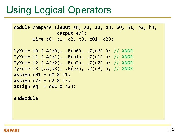
Using Logical Operators module compare (input a 0, a 1, a 2, a 3, b 0, b 1, b 2, b 3, output eq); wire c 0, c 1, c 2, c 3, c 01, c 23; My. Xnor assign i 0 (. A(a 0), . B(b 0), i 1 (. A(a 1), . B(b 1), i 2 (. A(a 2), . B(b 2), i 3 (. A(a 3), . B(b 3), c 01 = c 0 & c 1; c 23 = c 2 & c 3; eq = c 01 & c 23; . Z(c 0). Z(c 1). Z(c 2). Z(c 3) ); ); // // XNOR endmodule 135
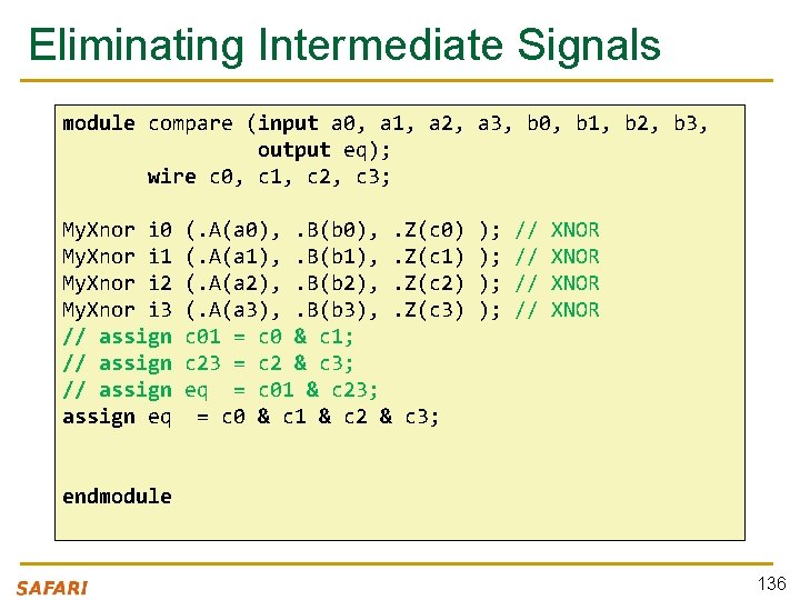
Eliminating Intermediate Signals module compare (input a 0, a 1, a 2, a 3, b 0, b 1, b 2, b 3, output eq); wire c 0, c 1, c 2, c 3; My. Xnor i 0 My. Xnor i 1 My. Xnor i 2 My. Xnor i 3 // assign eq (. A(a 0), . B(b 0), . Z(c 0) (. A(a 1), . B(b 1), . Z(c 1) (. A(a 2), . B(b 2), . Z(c 2) (. A(a 3), . B(b 3), . Z(c 3) c 01 = c 0 & c 1; c 23 = c 2 & c 3; eq = c 01 & c 23; = c 0 & c 1 & c 2 & c 3; ); ); // // XNOR endmodule 136
![Multi-Bit Signals (Bus) module compare (input [3: 0] a, input [3: 0] b, output Multi-Bit Signals (Bus) module compare (input [3: 0] a, input [3: 0] b, output](http://slidetodoc.com/presentation_image_h/2296460e6ab8856836ef54b82a439269/image-135.jpg)
Multi-Bit Signals (Bus) module compare (input [3: 0] a, input [3: 0] b, output eq); wire [3: 0] c; // bus definition My. Xnor i 0 i 1 i 2 i 3 assign eq (. A(a[0]), (. A(a[1]), (. A(a[2]), (. A(a[3]), . B(b[0]), . B(b[1]), . B(b[2]), . B(b[3]), . Z(c[0]). Z(c[1]). Z(c[2]). Z(c[3]) ); ); // // XNOR = &c; // short format endmodule 137
![Bitwise Operations module compare (input [3: 0] a, input [3: 0] b, output eq); Bitwise Operations module compare (input [3: 0] a, input [3: 0] b, output eq);](http://slidetodoc.com/presentation_image_h/2296460e6ab8856836ef54b82a439269/image-136.jpg)
Bitwise Operations module compare (input [3: 0] a, input [3: 0] b, output eq); wire [3: 0] c; // bus definition // // My. Xnor i 0 i 1 i 2 i 3 (. A(a[0]), (. A(a[1]), (. A(a[2]), (. A(a[3]), . B(b[0]), . B(b[1]), . B(b[2]), . B(b[3]), . Z(c[0]). Z(c[1]). Z(c[2]). Z(c[3]) ); ); assign c = ~(a ^ b); // XNOR assign eq = &c; // short format endmodule 138
![Highest Abstraction Level: Comparing Two Numbers module compare (input [3: 0] a, input [3: Highest Abstraction Level: Comparing Two Numbers module compare (input [3: 0] a, input [3:](http://slidetodoc.com/presentation_image_h/2296460e6ab8856836ef54b82a439269/image-137.jpg)
Highest Abstraction Level: Comparing Two Numbers module compare (input [3: 0] a, input [3: 0] b, output eq); // assign c = ~(a ^ b); // XNOR // assign eq = &c; // short format assign eq = (a == b) ? 1 : 0; // really short endmodule 139
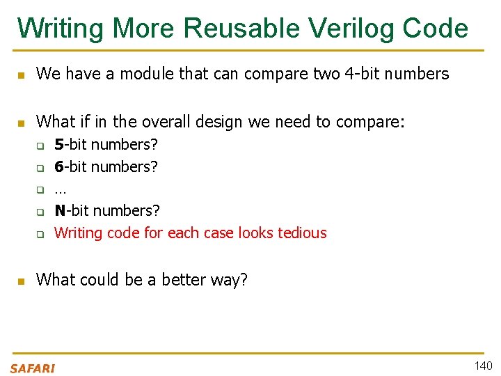
Writing More Reusable Verilog Code n We have a module that can compare two 4 -bit numbers n What if in the overall design we need to compare: q q q n 5 -bit numbers? 6 -bit numbers? … N-bit numbers? Writing code for each case looks tedious What could be a better way? 140
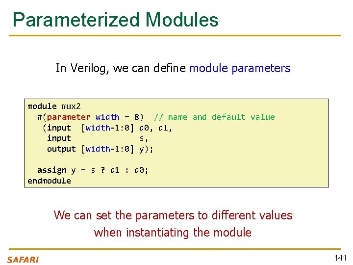
Parameterized Modules In Verilog, we can define module parameters module mux 2 #(parameter width = 8) // name and default value (input [width-1: 0] d 0, d 1, input s, output [width-1: 0] y); assign y = s ? d 1 : d 0; endmodule We can set the parameters to different values when instantiating the module 141
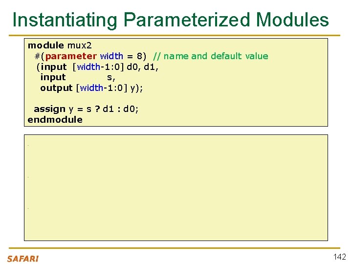
Instantiating Parameterized Modules module mux 2 #(parameter width = 8) // name and default value (input [width-1: 0] d 0, d 1, input s, output [width-1: 0] y); assign y = s ? d 1 : d 0; endmodule // If the parameter is not given, the default (8) is assumed mux 2 i_mux (d 0, d 1, s, out); // The same module with 12 -bit bus width: mux 2 #(12) i_mux_b (d 0, d 1, s, out); // A more verbose version: mux 2 #(. width(12)) i_mux_b (. d 0(d 0), . d 1(d 1), . s(s), . out(out)); 142
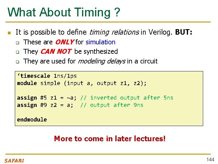
What About Timing ? n It is possible to define timing relations in Verilog. BUT: q These are ONLY for simulation q They CAN NOT be synthesized q They are used for modeling delays in a circuit ‘timescale 1 ns/1 ps module simple (input a, output z 1, z 2); assign #5 z 1 = ~a; // inverted output after 5 ns assign #9 z 2 = a; // output after 9 ns endmodule More to come in later lectures! 144
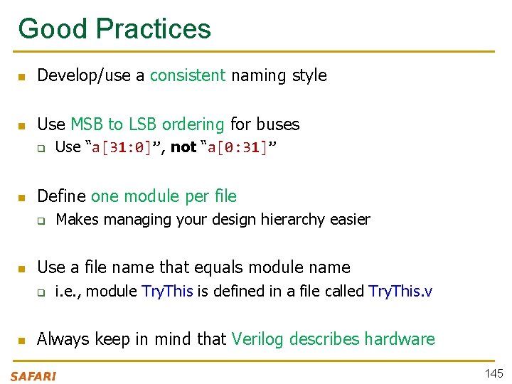
Good Practices n Develop/use a consistent naming style n Use MSB to LSB ordering for buses q n Define one module per file q n Makes managing your design hierarchy easier Use a file name that equals module name q n Use “a[31: 0]”, not “a[0: 31]” i. e. , module Try. This is defined in a file called Try. This. v Always keep in mind that Verilog describes hardware 145
Summary n We have seen an overview of Verilog n Discussed structural and behavioral modeling n Showed combinational logic constructs 146
- Slides: 143