Design of Digital Circuits Lecture 3 Introduction to

- Slides: 33

Design of Digital Circuits Lecture 3: Introduction to the Labs and FPGAs Prof. Onur Mutlu (Lecture by Hasan Hassan) ETH Zurich Spring 2018 1 March 2018 1

Lab Sessions n Where? q n HG E 19, HG E 26. 1, HG E 26. 3, HG E 27 When? q Tuesday 15: 15 -17: 00 (E 19, E 26. 1, E 26. 3) q Wednesday 15: 15 -17: 00 (E 26. 1, E 26. 3, E 27) q Friday 08: 15 -10: 00 (E 19, E 26. 3, E 27) q Friday 10: 15 -12: 00 (E 19, E 26. 3, E 27) 2

Grading n n 10 labs, 30 points in total We will put the lab manuals online q n https: //safari. ethz. ch/digitaltechnik/doku. php? id=labs Grading Policy q q q No need to hand in the reports! The assistants will check your work and note down your grade You should finish the labs within 1 week after they are announced n We want to help you successfully complete all the labs! n For questions q q Moodle Q&A (preferred) https: //moodleapp 2. let. ethz. ch/course/view. php? id=4352 digitaltechnik@lists. inf. ethz. ch 3

Agenda n Logistics n What We Will learn? n Overview of the Lab Exercises n Our FPGA Development Board q FPGA Microarchitecture n Programming an FPGA n Tutorial and Demo 4

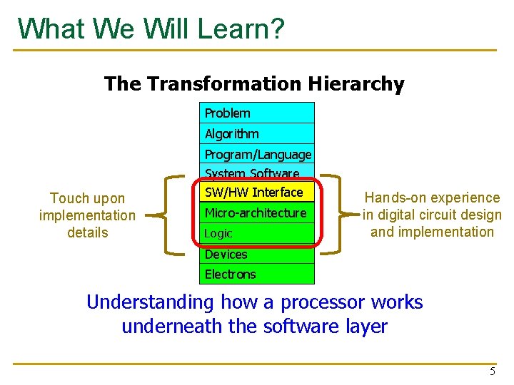
What We Will Learn? The Transformation Hierarchy Problem Algorithm Touch upon implementation details Program/Language System Software SW/HW Interface Micro-architecture Logic Hands-on experience in digital circuit design and implementation Devices Electrons Understanding how a processor works underneath the software layer 5

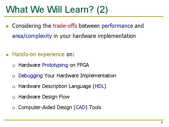
What We Will Learn? (2) n Considering the trade-offs between performance and area/complexity in your hardware implementation n Hands-on experience on: q Hardware Prototyping on FPGA q Debugging Your Hardware Implementation q Hardware Description Language (HDL) q Hardware Design Flow q Computer-Aided Design (CAD) Tools 6

Agenda n Logistics n What We Will learn? n Overview of the Lab Exercises n Our FPGA Development Board q FPGA Microarchitecture n Programming an FPGA n Tutorial and Demo 7

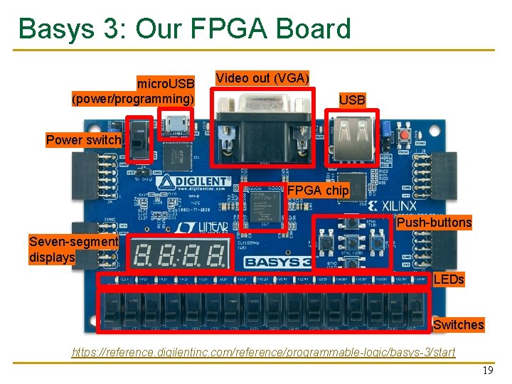
Basys 3: Our FPGA Board micro. USB (power/programming) Video out (VGA) USB Power switch FPGA chip Push-buttons Seven-segment displays LEDs Switches https: //reference. digilentinc. com/reference/programmable-logic/basys-3/start 8

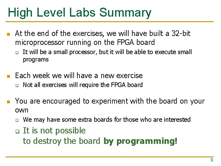
High Level Labs Summary n At the end of the exercises, we will have built a 32 -bit microprocessor running on the FPGA board q n Each week we will have a new exercise q n It will be a small processor, but it will be able to execute small programs Not all exercises will require the FPGA board You are encouraged to experiment with the board on your own q q We may have some extra boards for those who are interested It is not possible to destroy the board by programming! 9

Lab 1: Drawing a Basic Circuit n Comparison is a common operation in software programming q n n We usually want to know the relation between two variables (e. g. , <, >, ==, …) We will compare two electrical signals (inputs), and find whether they are same q The result (output) is also an electrical signal No FPGA programming involved q We encourage you to try later 10

Lab 2: Mapping Your Circuit to FPGA n Another common operation in software programming? q n n n Addition Design a circuit that adds two 1 -bit numbers Reuse the 1 -bit adder multiple times to perform 4 bit addition Implement the design on the FPGA board q q Input: switches Output: LEDs 11

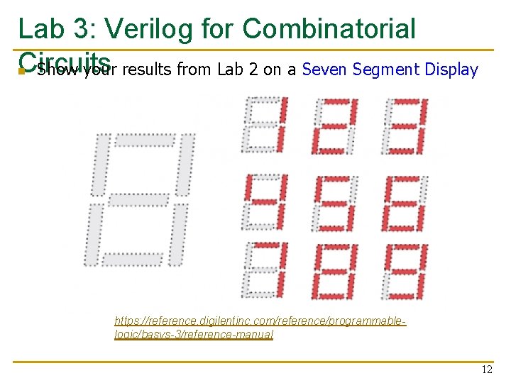
Lab 3: Verilog for Combinatorial Circuits n Show your results from Lab 2 on a Seven Segment Display https: //reference. digilentinc. com/reference/programmablelogic/basys-3/reference-manual 12

Lab 4: Finite State Machines n Blinking LEDs for a car’s turn signals q Implement and use memories q Change the blinking speed 13

Lab 5: Implementing an ALU n Towards implementing your very first processor n Implement your own Arithmetic and Logic Unit (ALU) n An ALU is an important part of the CPU q q Arithmetic operations: add, subtract, multiply, compare, … Logic operations: AND, OR, … 14

Lab 6: Testing the ALU n n Simulate your design from Lab 5 Learn how to debug your implementation to resolve problems 15

Lab 7: Writing Assembly Code n Programming in assembly language q n n MIPS Implement a program which you will later use to run on your processor Image manipulation 16

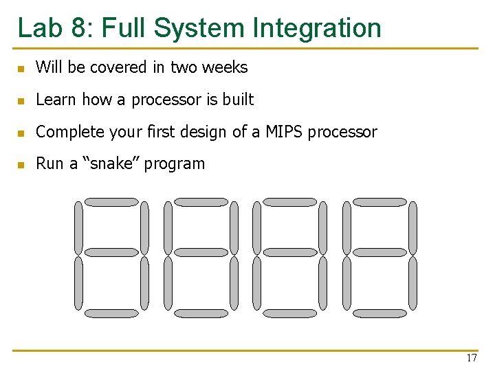
Lab 8: Full System Integration n Will be covered in two weeks n Learn how a processor is built n Complete your first design of a MIPS processor n Run a “snake” program 17

Lab 9: The Performance of MIPS n Improve the performance of your processor from Lab 8 by adding new instructions q Multiplication q Bit shifting 18

Basys 3: Our FPGA Board micro. USB (power/programming) Video out (VGA) USB Power switch FPGA chip Push-buttons Seven-segment displays LEDs Switches https: //reference. digilentinc. com/reference/programmable-logic/basys-3/start 19

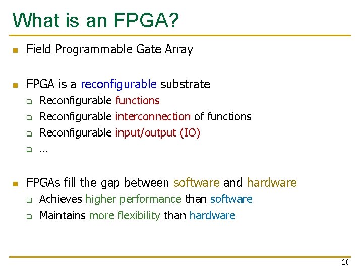
What is an FPGA? n Field Programmable Gate Array n FPGA is a reconfigurable substrate q q n Reconfigurable functions Reconfigurable interconnection of functions Reconfigurable input/output (IO) … FPGAs fill the gap between software and hardware q q Achieves higher performance than software Maintains more flexibility than hardware 20

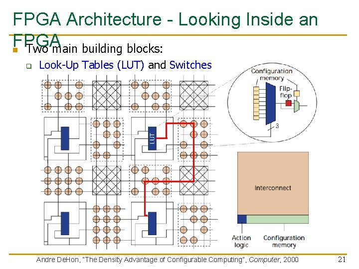
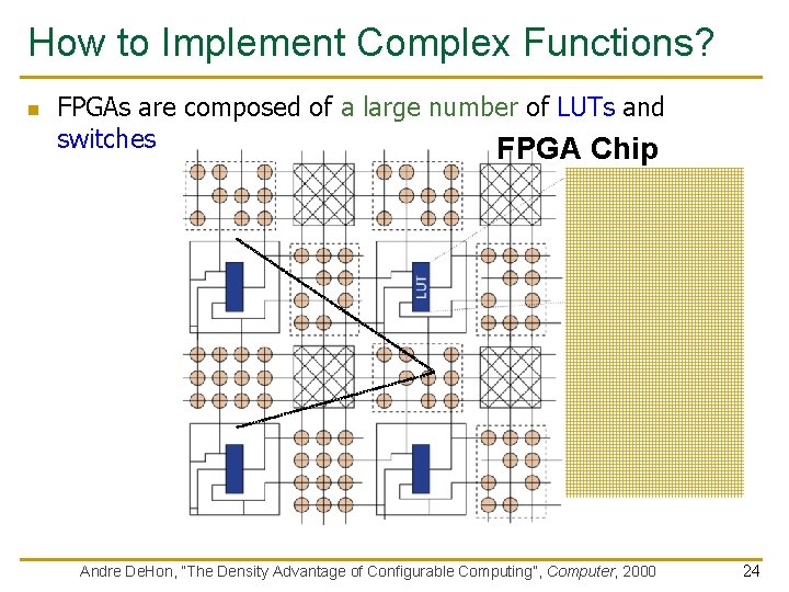
FPGA Architecture - Looking Inside an FPGA n Two main building blocks: q Look-Up Tables (LUT) and Switches Andre De. Hon, “The Density Advantage of Configurable Computing”, Computer, 2000 21

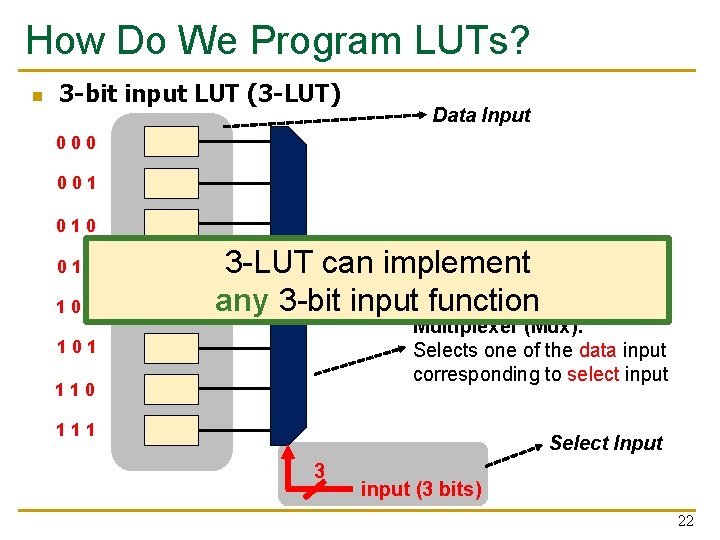
How Do We Program LUTs? n 3 -bit input LUT (3 -LUT) Data Input 000 001 010 011 100 3 -LUT can implement output (1 bit) any 3 -bit input function Multiplexer (Mux): Selects one of the data input corresponding to select input 101 110 111 Select Input 3 input (3 bits) 22

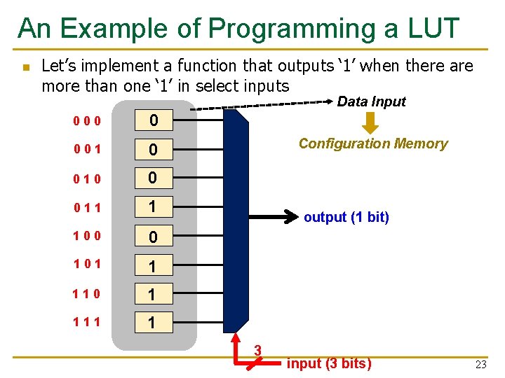
An Example of Programming a LUT n Let’s implement a function that outputs ‘ 1’ when there are more than one ‘ 1’ in select inputs Data Input 000 0 001 0 010 0 011 1 100 0 101 1 110 1 111 1 Configuration Memory output (1 bit) 3 input (3 bits) 23

How to Implement Complex Functions? n FPGAs are composed of a large number of LUTs and switches FPGA Chip Andre De. Hon, “The Density Advantage of Configurable Computing”, Computer, 2000 24

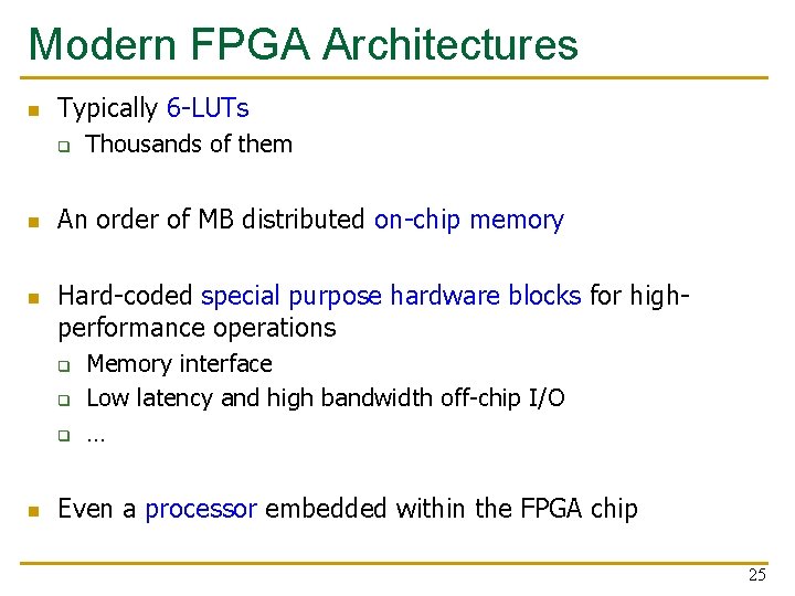
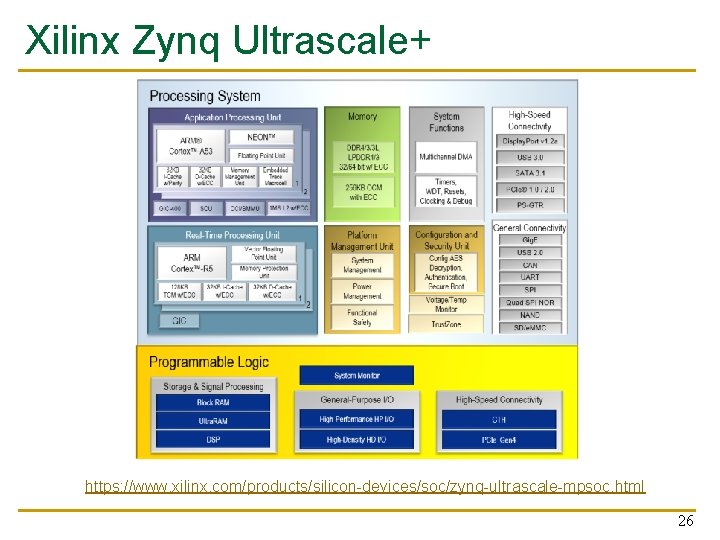
Modern FPGA Architectures n Typically 6 -LUTs q n n An order of MB distributed on-chip memory Hard-coded special purpose hardware blocks for highperformance operations q q q n Thousands of them Memory interface Low latency and high bandwidth off-chip I/O … Even a processor embedded within the FPGA chip 25

Xilinx Zynq Ultrascale+ https: //www. xilinx. com/products/silicon-devices/soc/zynq-ultrascale-mpsoc. html 26

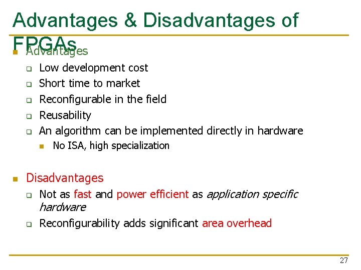
Advantages & Disadvantages of FPGAs n Advantages q q q Low development cost Short time to market Reconfigurable in the field Reusability An algorithm can be implemented directly in hardware n n No ISA, high specialization Disadvantages q Not as fast and power efficient as application specific hardware q Reconfigurability adds significant area overhead 27

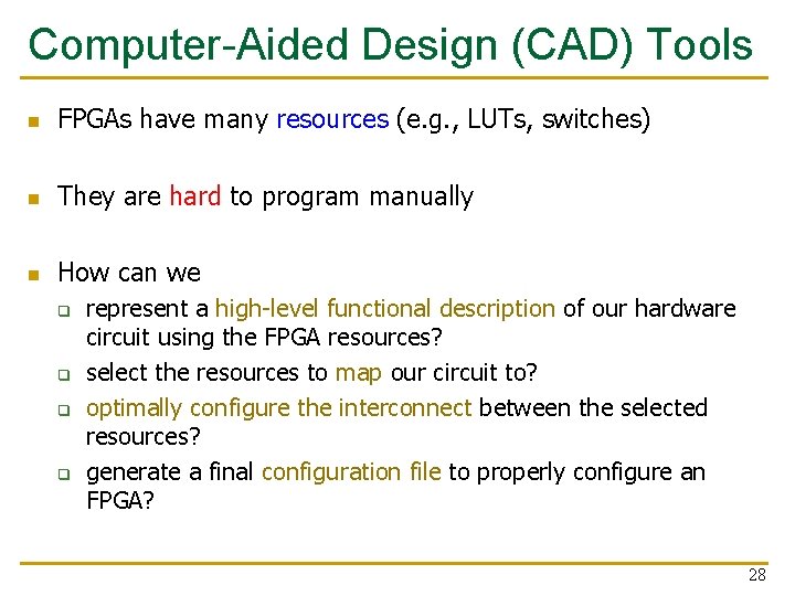
Computer-Aided Design (CAD) Tools n FPGAs have many resources (e. g. , LUTs, switches) n They are hard to program manually n How can we q q represent a high-level functional description of our hardware circuit using the FPGA resources? select the resources to map our circuit to? optimally configure the interconnect between the selected resources? generate a final configuration file to properly configure an FPGA? 28

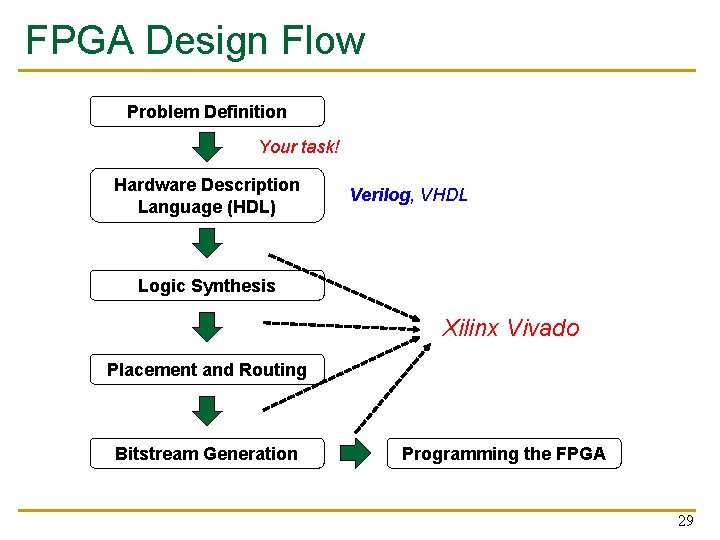
FPGA Design Flow Problem Definition Your task! Hardware Description Language (HDL) Verilog, VHDL Logic Synthesis Xilinx Vivado Placement and Routing Bitstream Generation Programming the FPGA 29

Vivado n n IDE-like software that helps us throughout the FPGA design flow Provides tools to simulate our designs q q n n Validate the correctness of the implementation Debugging Provides drivers and graphical interface to easily program the FPGA using a USB cable Installed in computer rooms in HG (E 19, E 26. 1, E 26. 3, E 27) 30

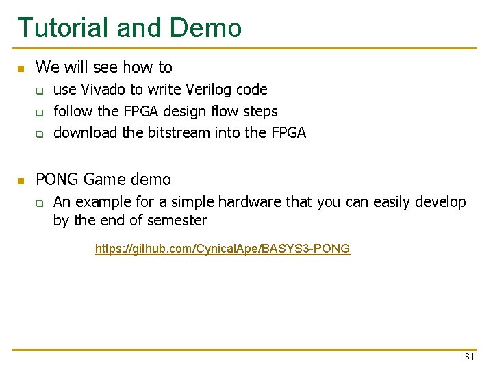
Tutorial and Demo n We will see how to q q q n use Vivado to write Verilog code follow the FPGA design flow steps download the bitstream into the FPGA PONG Game demo q An example for a simple hardware that you can easily develop by the end of semester https: //github. com/Cynical. Ape/BASYS 3 -PONG 31

What We Have Covered Today? n Logistics n What We Will learn? n Overview of the Lab Exercises n Our FPGA Development Board q FPGA Microarchitecture n Programming an FPGA n Tutorial and Demo 32

Design of Digital Circuits Lecture 3: Introduction to the Labs and FPGAs Prof. Onur Mutlu (Lecture by Hasan Hassan) ETH Zurich Spring 2018 1 March 2018 33