Design of Digital Circuits Lab 2 Supplement Mapping

Design of Digital Circuits Lab 2 Supplement: Mapping Your Circuit to FPGA Prof. Onur Mutlu ETH Zurich Spring 2019 12 March 2019
What Will We Learn? n In Lab 2, you will learn how to map your circuits to an FPGA. n Design a 4 -bit adder. q Design a 1 -bit full-adder. q Use full-adders to design a 4 -bit adder. n Program your FPGA using Vivado software for HDL design. n Work with your FPGA board and see the results of your designs on the FPGA output (in this case LEDs). 2
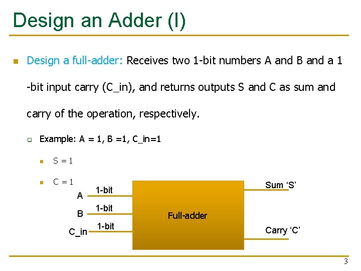
Design an Adder (I) n Design a full-adder: Receives two 1 -bit numbers A and B and a 1 -bit input carry (C_in), and returns outputs S and C as sum and carry of the operation, respectively. q Example: A = 1, B =1, C_in=1 n S=1 n C=1 A B C_in Sum ‘S’ 1 -bit Full-adder Carry ‘C’ 3
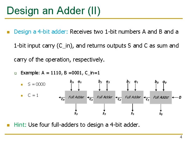
Design an Adder (II) n Design a 4 -bit adder: Receives two 1 -bit numbers A and B and a 1 -bit input carry (C_in), and returns outputs S and C as sum and carry of the operation, respectively. q n Example: A = 1110, B =0001, C_in=1 n S = 0000 n C=1 Hint: Use four full-adders to design a 4 -bit adder. 4
Design an Adder (Overview) 1. You will use truth tables to derive the Boolean equation of the adder. 2. You will design the schematic of the circuit using logic gates. 3. In the next step, you will use Vivado to write your design in Verilog. 4. In the end, you will use Vivado to program the FPGA. 5
Vivado n n n For this course, we use the software Vivado for FPGA programming. The computers in the lab rooms are already installed with the necessary software. If you wish to use your own computer, you can refer to the following instructions: q https: //reference. digilentinc. com/learn/programmablelogic/tutorials/basys-3 -getting-started/start 6

Verilog 7
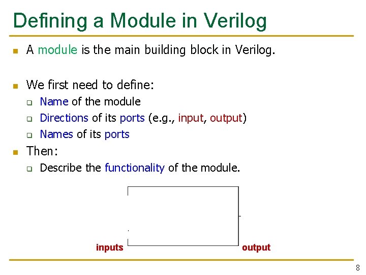
Defining a Module in Verilog n A module is the main building block in Verilog. n We first need to define: q q q n Name of the module Directions of its ports (e. g. , input, output) Names of its ports Then: q Describe the functionality of the module. example inputs output 8
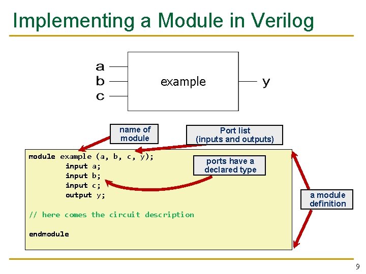
Implementing a Module in Verilog example name of module example (a, b, c, y); input a; input b; input c; output y; Port list (inputs and outputs) ports have a declared type a module definition // here comes the circuit description endmodule 9
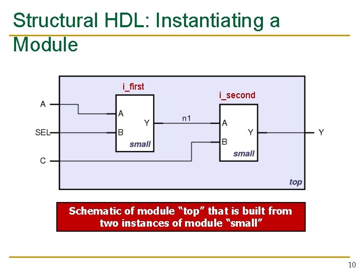
Structural HDL: Instantiating a Module i_first i_second Schematic of module “top” that is built from two instances of module “small” 10
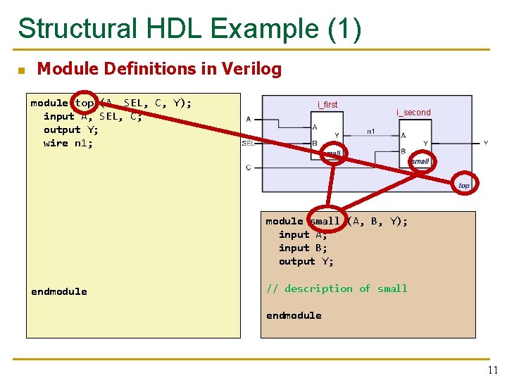
Structural HDL Example (1) n Module Definitions in Verilog module top (A, SEL, C, Y); input A, SEL, C; output Y; wire n 1; i_first i_second module small (A, B, Y); input A; input B; output Y; endmodule // description of small endmodule 11
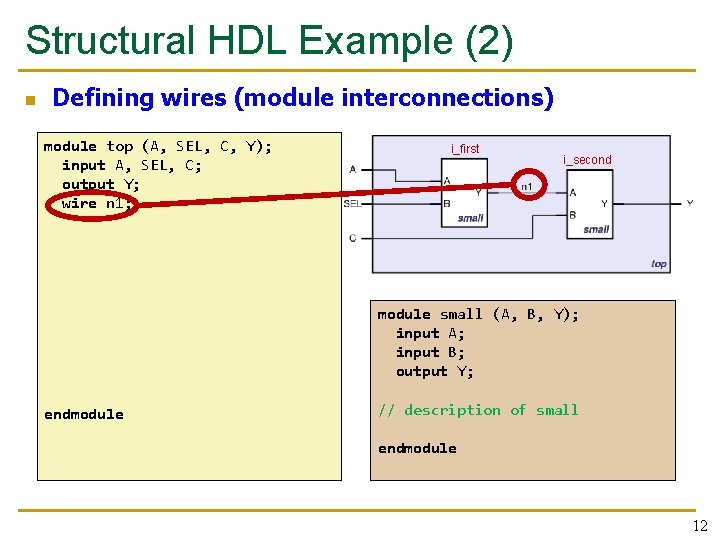
Structural HDL Example (2) n Defining wires (module interconnections) module top (A, SEL, C, Y); input A, SEL, C; output Y; wire n 1; i_first i_second module small (A, B, Y); input A; input B; output Y; endmodule // description of small endmodule 12
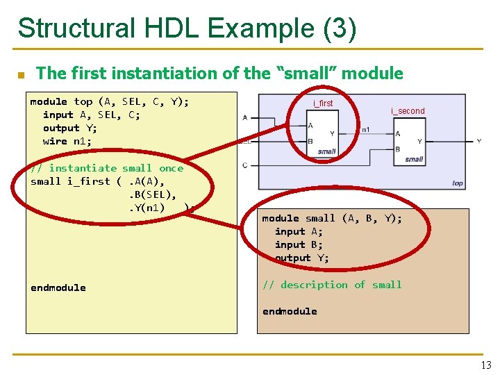
Structural HDL Example (3) n The first instantiation of the “small” module top (A, SEL, C, Y); input A, SEL, C; output Y; wire n 1; // instantiate small once small i_first (. A(A), . B(SEL), . Y(n 1) ); endmodule i_first i_second module small (A, B, Y); input A; input B; output Y; // description of small endmodule 13
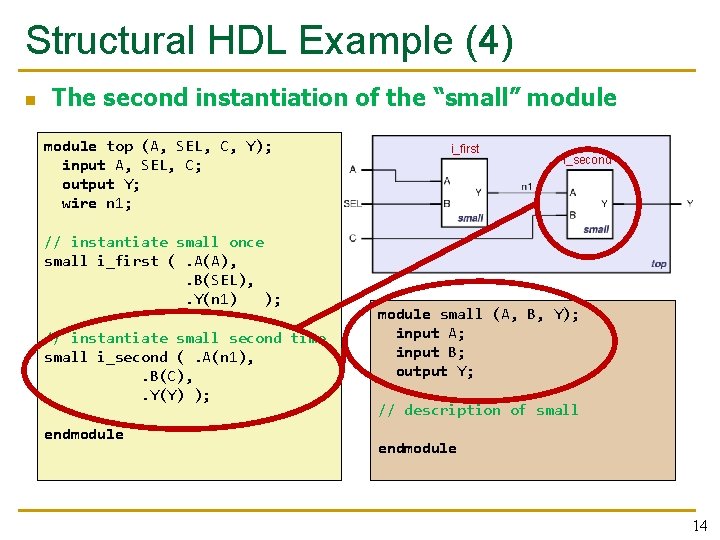
Structural HDL Example (4) n The second instantiation of the “small” module top (A, SEL, C, Y); input A, SEL, C; output Y; wire n 1; // instantiate small once small i_first (. A(A), . B(SEL), . Y(n 1) ); // instantiate small second time small i_second (. A(n 1), . B(C), . Y(Y) ); endmodule i_first i_second module small (A, B, Y); input A; input B; output Y; // description of small endmodule 14
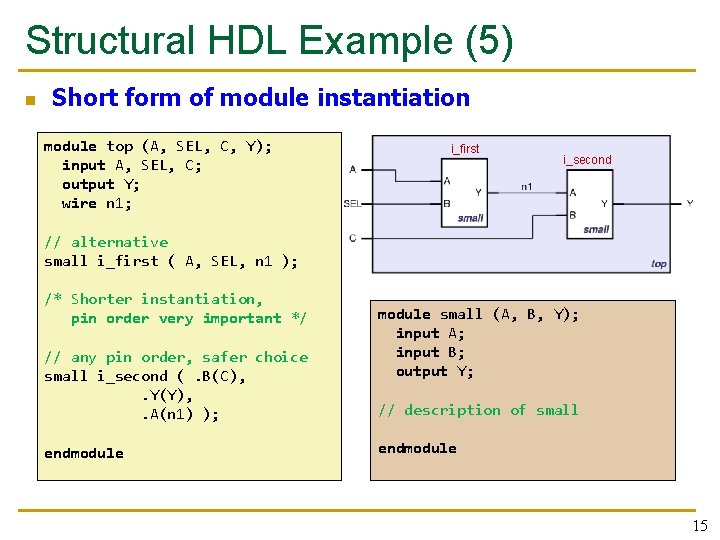
Structural HDL Example (5) n Short form of module instantiation module top (A, SEL, C, Y); input A, SEL, C; output Y; wire n 1; i_first i_second // alternative small i_first ( A, SEL, n 1 ); /* Shorter instantiation, pin order very important */ // any pin order, safer choice small i_second (. B(C), . Y(Y), . A(n 1) ); endmodule small (A, B, Y); input A; input B; output Y; // description of small endmodule 15
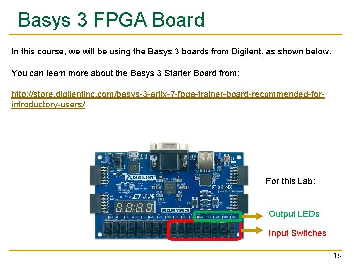
Basys 3 FPGA Board In this course, we will be using the Basys 3 boards from Digilent, as shown below. You can learn more about the Basys 3 Starter Board from: http: //store. digilentinc. com/basys-3 -artix-7 -fpga-trainer-board-recommended-forintroductory-users/ For this Lab: Output LEDs Input Switches 16
Last Words n In this lab, you will map your circuit to an FPGA. n First you will design a 4 -bit adder. n n n Then, you will learn how to use Xilinx Vivado for writing Verilog and how to connect to the Basys 3 board. Finally, you will program the FPGA and get the circuit running on the FPGA board. You will find more exercises in the lab report. 17

Design of Digital Circuits Lab 2 Supplement: Mapping Your Circuit to FPGA Prof. Onur Mutlu ETH Zurich Spring 2019 12 March 2019
- Slides: 18