Design Of Combinational Logic Circuits ACOE 161 Digital
Design Of Combinational Logic Circuits ACOE 161 Digital Circuit Design 1

Design of combinational digital circuits • Steps to design a combinational digital circuit: – – From the problem statement derive the truth table From the truth table derive the unsimplified logic expression Simplify the logic expression From the simplified expression draw the logic circuit • Example: Design a 3 -input (A, B, C) digital circuit that will give at its output (X) a logic 1 only if the binary number formed at the input has more ones than zeros. ACOE 161 Digital Circuit Design 2

Design of combinational digital circuits (Cont. ) • Example: Design a 4 -input (A, B, C, D) digital circuit that will give at its output (X) a logic 1 only if the binary number formed at the input is between 2 and 9 (including). ACOE 161 Digital Circuit Design 3
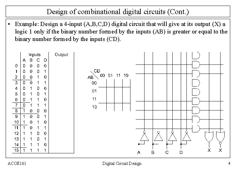
Design of combinational digital circuits (Cont. ) • Example: Design a 4 -input (A, B, C, D) digital circuit that will give at its output (X) a logic 1 only if the binary number formed by the inputs (AB) is greater or equal to the binary number formed by the inputs (CD). ACOE 161 Digital Circuit Design 4
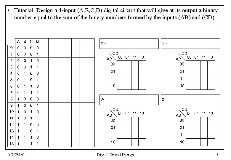
• Tutorial: Design a 4 -input (A, B, C, D) digital circuit that will give at its output a binary number equal to the sum of the binary numbers formed by the inputs (AB) and (CD). ACOE 161 Digital Circuit Design 5

ACOE 161 Digital Circuit Design 6
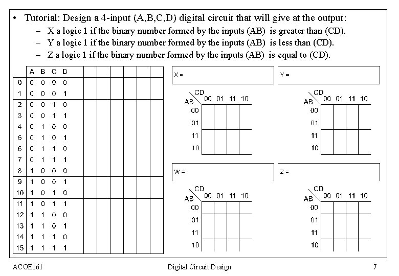
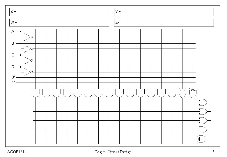
• Tutorial: Design a 4 -input (A, B, C, D) digital circuit that will give at the output: – X a logic 1 if the binary number formed by the inputs (AB) is greater than (CD). – Y a logic 1 if the binary number formed by the inputs (AB) is less than (CD). – Z a logic 1 if the binary number formed by the inputs (AB) is equal to (CD). ACOE 161 Digital Circuit Design 7
ACOE 161 Digital Circuit Design 8
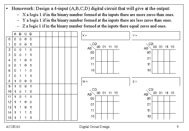
• Homework: Design a 4 -input (A, B, C, D) digital circuit that will give at the output: – X a logic 1 if in the binary number formed at the inputs there are more zeros than ones. – Y a logic 1 if in the binary number formed at the inputs there are less zeros than ones. – Z a logic 1 if in the binary number formed at the inputs there equal zeros and ones. ACOE 161 Digital Circuit Design 9

ACOE 161 Digital Circuit Design 10
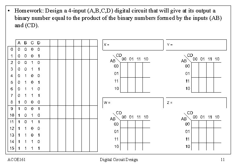
• Homework: Design a 4 -input (A, B, C, D) digital circuit that will give at its output a binary number equal to the product of the binary numbers formed by the inputs (AB) and (CD). ACOE 161 Digital Circuit Design 11

ACOE 161 Digital Circuit Design 12
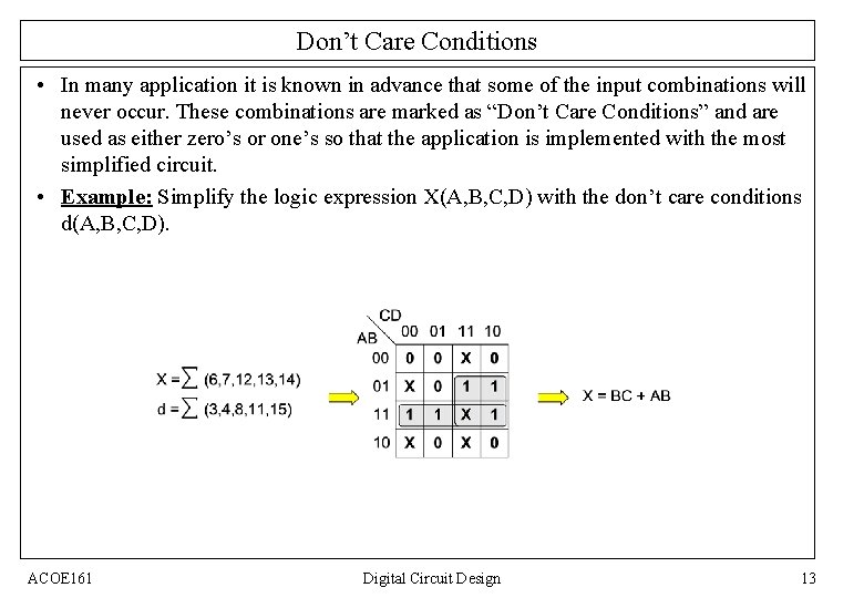
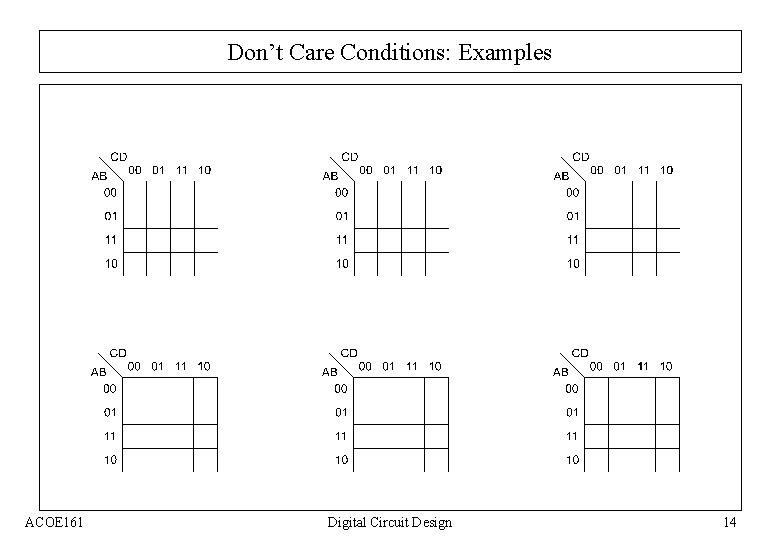
Don’t Care Conditions • In many application it is known in advance that some of the input combinations will never occur. These combinations are marked as “Don’t Care Conditions” and are used as either zero’s or one’s so that the application is implemented with the most simplified circuit. • Example: Simplify the logic expression X(A, B, C, D) with the don’t care conditions d(A, B, C, D). ACOE 161 Digital Circuit Design 13
Don’t Care Conditions: Examples ACOE 161 Digital Circuit Design 14
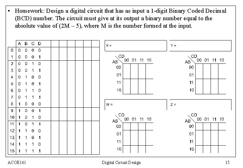
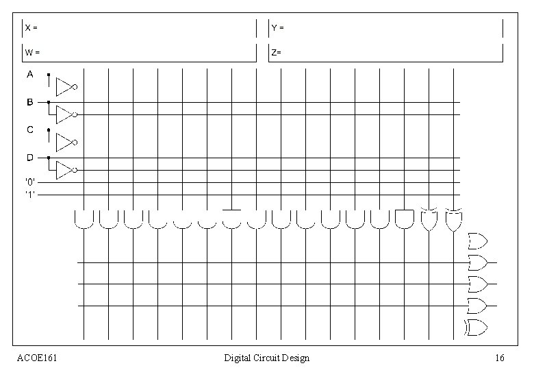
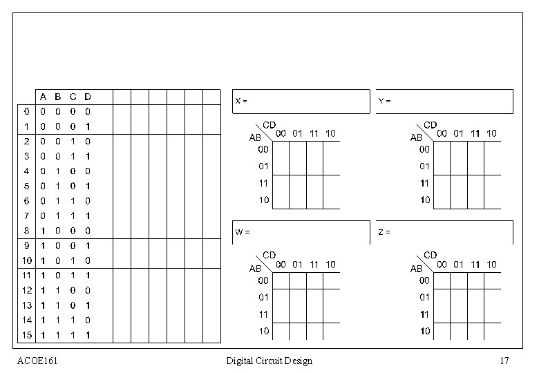
• Homework: Design a digital circuit that has as input a 1 -digit Binary Coded Decimal (BCD) number. The circuit must give at its output a binary number equal to the absolute value of (2 M – 5), where M is the number formed at the input. ACOE 161 Digital Circuit Design 15
ACOE 161 Digital Circuit Design 16
ACOE 161 Digital Circuit Design 17

ACOE 161 Digital Circuit Design 18
Mapping to NAND gates • Assumptions: – Gate loading and delay are ignored – Cell library contains an inverter and n-input NAND gates, n = 2, 3, … – An AND, OR, inverter schematic for the circuit is available • The mapping is accomplished by: – Replacing AND and OR symbols, – Pushing inverters through circuit fan-out points, and – Canceling inverter pairs ACOE 161 Digital Circuit Design 19
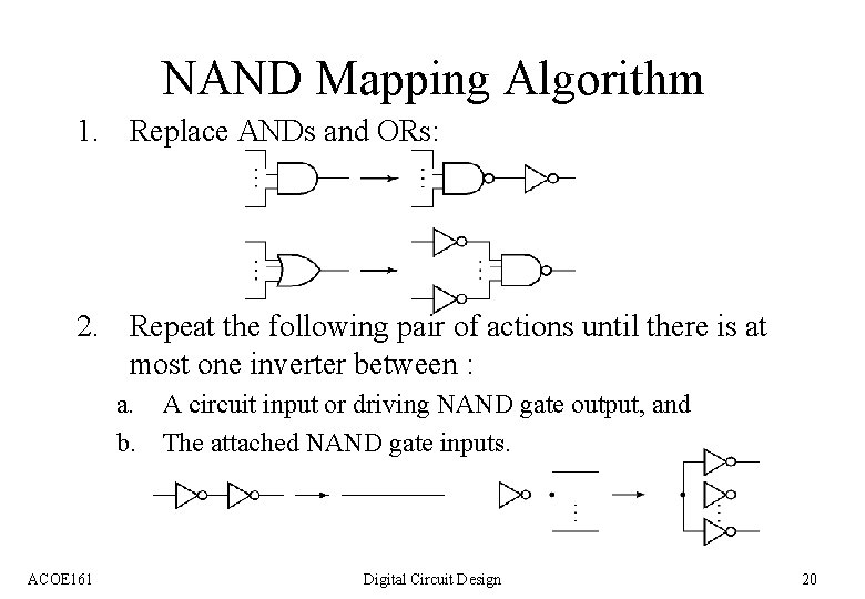
NAND Mapping Algorithm 1. Replace ANDs and ORs: 2. Repeat the following pair of actions until there is at most one inverter between : a. A circuit input or driving NAND gate output, and b. The attached NAND gate inputs. ACOE 161 Digital Circuit Design 20
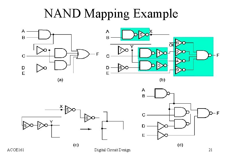
NAND Mapping Example ACOE 161 Digital Circuit Design 21

Mapping to NOR gates • Assumptions: – Gate loading and delay are ignored – Cell library contains an inverter and n-input NOR gates, n = 2, 3, … – An AND, OR, inverter schematic for the circuit is available • The mapping is accomplished by: – Replacing AND and OR symbols, – Pushing inverters through circuit fan-out points, and – Canceling inverter pairs ACOE 161 Digital Circuit Design 22
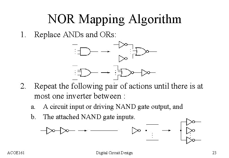
NOR Mapping Algorithm 1. Replace ANDs and ORs: 2. Repeat the following pair of actions until there is at most one inverter between : a. A circuit input or driving NAND gate output, and b. The attached NAND gate inputs. ACOE 161 Digital Circuit Design 23
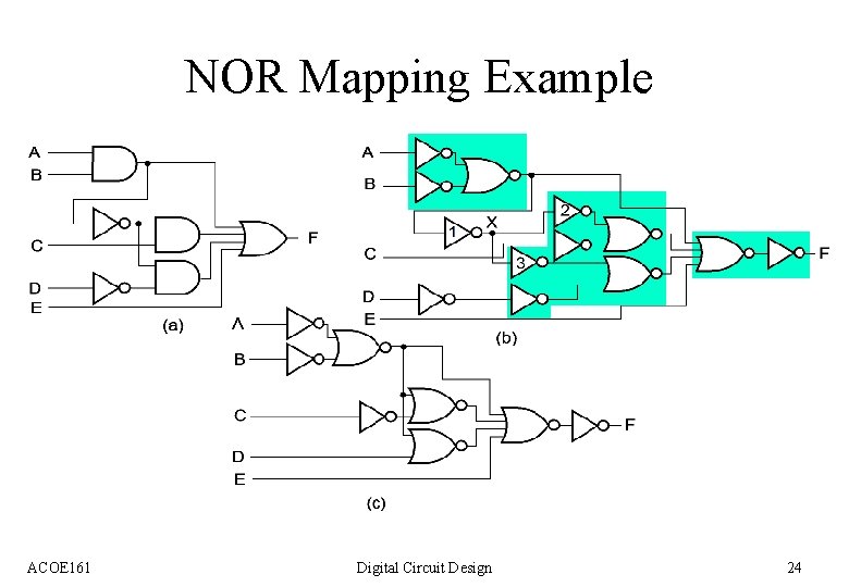
NOR Mapping Example ACOE 161 Digital Circuit Design 24
- Slides: 24