Design of a Solid State Power Amplifier for
- Slides: 30

Design of a Solid State Power Amplifier for a H+ ECR Ion Source at 2. 7 GHz Pedro J. González, RF Group, ESS-Bilbao TIARA Workshop on RF Power Generation for Accelerators 17 -19 June 2013 Ångström Laboratory, Uppsala (Sweden)

Contents • ISHP: ESS Bilbao H+ ECR Ion Source • Description • ISHP Microwave System • Block Diagram • Klystron Amplifier, RFGEN, ATU, Control • Why an SSPA? • SSPA Design • Redundancy Configurations • 1: 2 Phase Combined Redundancy System • 1 -k. W Module • WG Switches and Components • Power Supplies / Control • Phase Matching • Bibliography • Acknowledgements

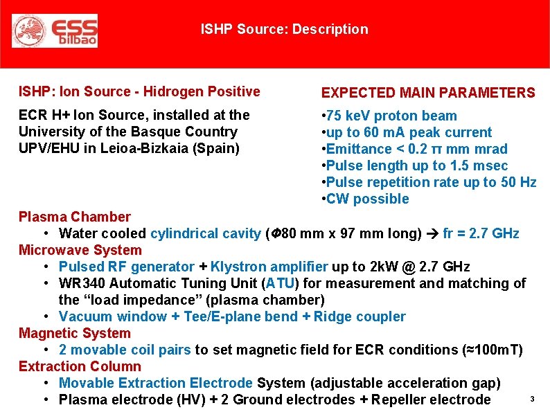
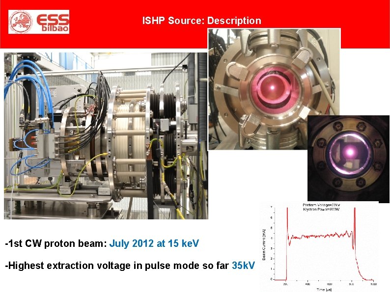
ISHP Source: Description ISHP: Ion Source - Hidrogen Positive EXPECTED MAIN PARAMETERS ECR H+ Ion Source, installed at the University of the Basque Country UPV/EHU in Leioa-Bizkaia (Spain) • 75 ke. V proton beam • up to 60 m. A peak current • Emittance < 0. 2 π mm mrad • Pulse length up to 1. 5 msec • Pulse repetition rate up to 50 Hz • CW possible Plasma Chamber • Water cooled cylindrical cavity (Ф 80 mm x 97 mm long) fr = 2. 7 GHz Microwave System • Pulsed RF generator + Klystron amplifier up to 2 k. W @ 2. 7 GHz • WR 340 Automatic Tuning Unit (ATU) for measurement and matching of the “load impedance” (plasma chamber) • Vacuum window + Tee/E-plane bend + Ridge coupler Magnetic System • 2 movable coil pairs to set magnetic field for ECR conditions (≈100 m. T) Extraction Column • Movable Extraction Electrode System (adjustable acceleration gap) 3 • Plasma electrode (HV) + 2 Ground electrodes + Repeller electrode

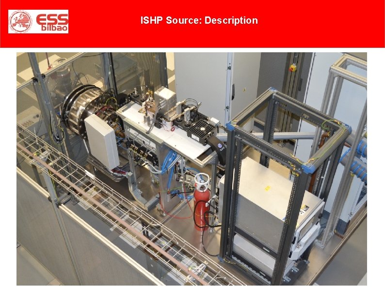
ISHP Source: Description

ISHP Source: Description -1 st CW proton beam: July 2012 at 15 ke. V -Highest extraction voltage in pulse mode so far 35 k. V

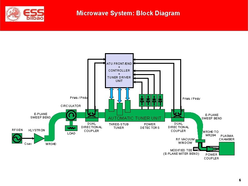
Microwave System: Block Diagram ATU FRONT/END + CONTROLLER + TUNER DRIVER UNIT PFWD / PREV E-PLANE SWEEP BEND RFGEN KLYSTRON Coax R E-PLANE SWEEP BEND AUTOMATIC TUNER UNIT LOAD WR 340 F R F CIRCULATOR DUAL DIRECTIONAL COUPLER THREE-STUB TUNER POWER DETECTORS DUAL DIRECTIONAL COUPLER RF VACUUM WINDOW MODIFIED TEE (E-PLANE MITER BEND) WR 340 TO WR 284 PLASMA CHAMBER POWER COUPLER 6

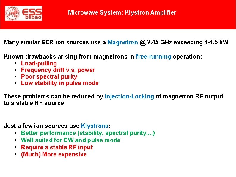
Microwave System: Klystron Amplifier Many similar ECR ion sources use a Magnetron @ 2. 45 GHz exceeding 1 -1. 5 k. W Known drawbacks arising from magnetrons in free-running operation: • Load-pulling • Frequency drift v. s. power • Poor spectral purity • Low stability in pulse mode These problems can be reduced by Injection-Locking of magnetron RF output to a stable RF source Just a few ion sources use Klystrons: • Better performance (stability, spectral purity, . . . ) • Well suited for CW and pulse mode • Require a stable RF input • (Much) More expensive

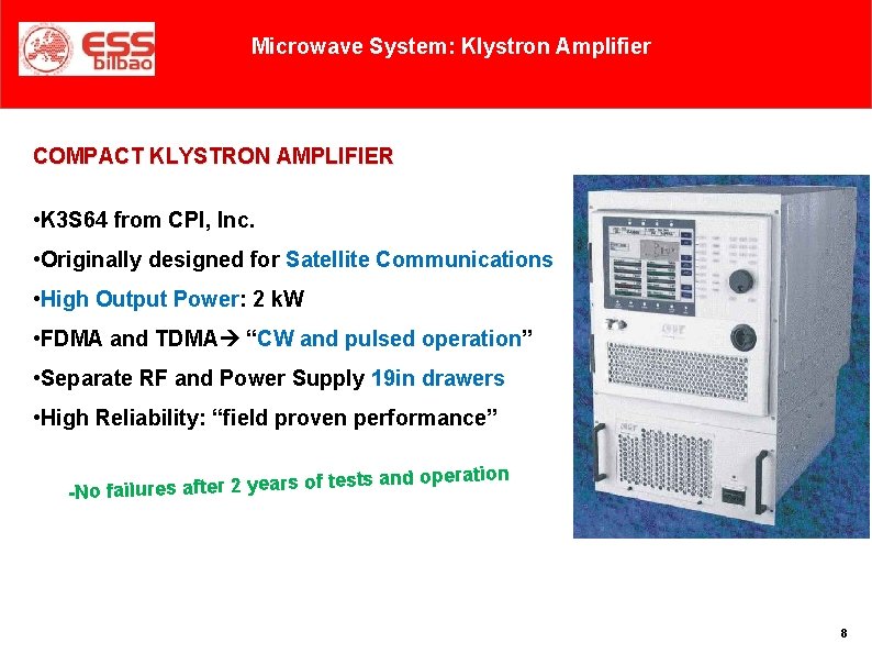
Microwave System: Klystron Amplifier COMPACT KLYSTRON AMPLIFIER • K 3 S 64 from CPI, Inc. • Originally designed for Satellite Communications • High Output Power: 2 k. W • FDMA and TDMA “CW and pulsed operation” • Separate RF and Power Supply 19 in drawers • High Reliability: “field proven performance” s of tests -No failures after 2 year and operation 8

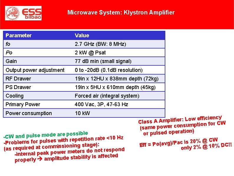
Microwave System: Klystron Amplifier Parameter Value fo 2. 7 GHz (BW: 8 MHz) Po 2 k. W @ Psat Gain 77 d. B min (small signal) Output power adjustment 0 to -20 d. B (0. 1 d. B resolution) RF Drawer 19 in x 12 HU x 838 mm depth (72 kg) PS Drawer 19 in x 5 HU x 610 mm depth (45 kg) Cooling Forced air (integral system) Primary Power 400 Vac, 3 P, 47 -63 Hz Power consumption 10 k. W e possible -CW and pulse mode ar rate <10 Hz n io it et p re h it w es ls u p -Problems for ning stage): o si is m m co at ed ir u q (as re not respond o d s er et m er w o p k ea -internal p ability is affected properly amplitude st efficiency w o L r: e fi li p m A A Class tion for CW p m u s n o c r e w o p (same n) or pulsed operatio @ CW % 0 2 is c a P )/ g v Eff = Po(a DC!! only 2% @ 10%

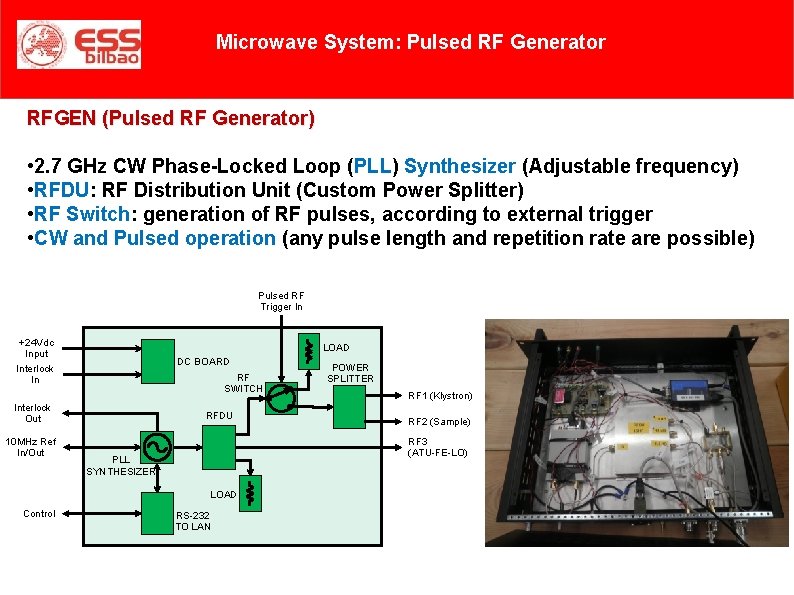
Microwave System: Pulsed RF Generator RFGEN (Pulsed RF Generator) • 2. 7 GHz CW Phase-Locked Loop (PLL) Synthesizer (Adjustable frequency) • RFDU: RF Distribution Unit (Custom Power Splitter) • RF Switch: generation of RF pulses, according to external trigger • CW and Pulsed operation (any pulse length and repetition rate are possible) Pulsed RF Trigger In +24 Vdc Input Interlock In LOAD DC BOARD RF SWITCH Interlock Out 10 MHz Ref In/Out RFDU RF 1 (Klystron) RF 2 (Sample) RF 3 (ATU-FE-LO) PLL SYNTHESIZER LOAD Control POWER SPLITTER RS-232 TO LAN

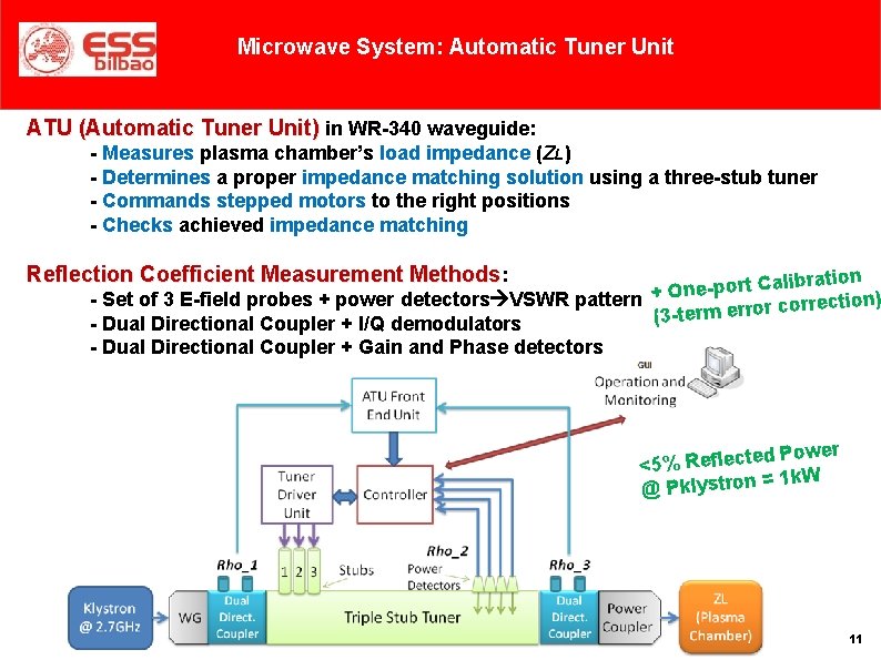
Microwave System: Automatic Tuner Unit ATU (Automatic Tuner Unit) in WR-340 waveguide: - Measures plasma chamber’s load impedance (ZL) - Determines a proper impedance matching solution using a three-stub tuner - Commands stepped motors to the right positions - Checks achieved impedance matching Reflection Coefficient Measurement Methods: bration li a C t r o -p e n - Set of 3 E-field probes + power detectors VSWR pattern + O ection) r r o c r o r r e m (3 -ter - Dual Directional Coupler + I/Q demodulators - Dual Directional Coupler + Gain and Phase detectors ower P d te c e fl e R <5% = 1 k. W @ Pklystron 11

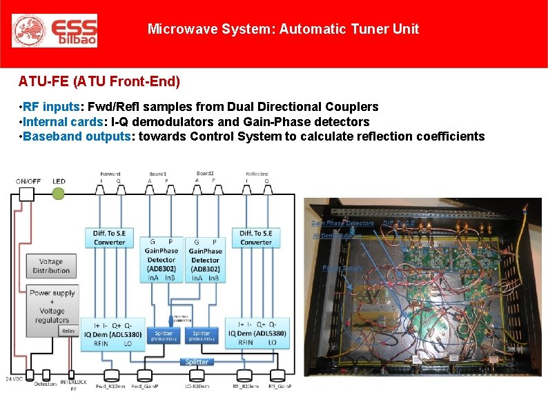
Microwave System: Automatic Tuner Unit ATU-FE (ATU Front-End) • RF inputs: Fwd/Refl samples from Dual Directional Couplers • Internal cards: I-Q demodulators and Gain-Phase detectors • Baseband outputs: towards Control System to calculate reflection coefficients

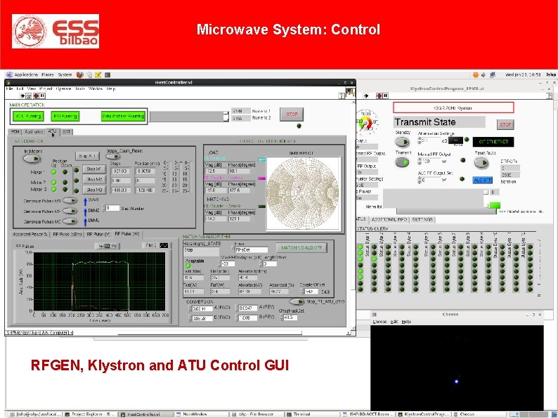
Microwave System: Control RFGEN, Klystron and ATU Control GUI

Microwave System: Why an SSPA? Why a solid state replacement for tube amplifiers? SSPA: Solid State Power Amplifier • Cost-Effective Solution • Lower Cost of Spares • Smaller Size and Weight • Higher Efficiency in Pulse Mode Energy and cost saving • More Reliable (? ? ) Predicted MTBF SSPA >> Tubes (20, 000 - 50, 000 hours) • No HV Power Supplies Required The Tube Guy: “Most SSPA systems are redundant, include redundant hot-swappable power supplies and justify high reliability figures. That suggests there is a major problem!” Increasing number of manufacturers of power transistors and amplifiers (LDMOS, Ga. N HEMT), providing higher power levels (even hundreds of Watts up to 3 GHz), for ISM (2. 45 GHz) and S-Band RADAR (2. 7 -3. 5 GHz) applications (markets traditionally served by tubes such as magnetrons, klystrons or TWTs) e. g. : NXP, Freescale, RFHIC, Cree, Sumitomo, Toshiba, Nitronex, Triquint, RFMD, . . . 14

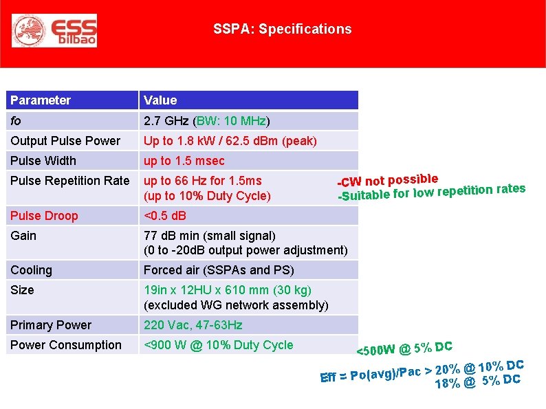
SSPA: Specifications Parameter Value fo 2. 7 GHz (BW: 10 MHz) Output Pulse Power Up to 1. 8 k. W / 62. 5 d. Bm (peak) Pulse Width up to 1. 5 msec Pulse Repetition Rate up to 66 Hz for 1. 5 ms (up to 10% Duty Cycle) Pulse Droop <0. 5 d. B Gain 77 d. B min (small signal) (0 to -20 d. B output power adjustment) Cooling Forced air (SSPAs and PS) Size 19 in x 12 HU x 610 mm (30 kg) (excluded WG network assembly) Primary Power 220 Vac, 47 -63 Hz Power Consumption <900 W @ 10% Duty Cycle -CW not possible ion rates it et p re w lo r fo le ab it u -S <500 W @ 5% DC @ 10% DC % 0 2 > c a P )/ g v (a Eff = Po 18% @ 5% DC

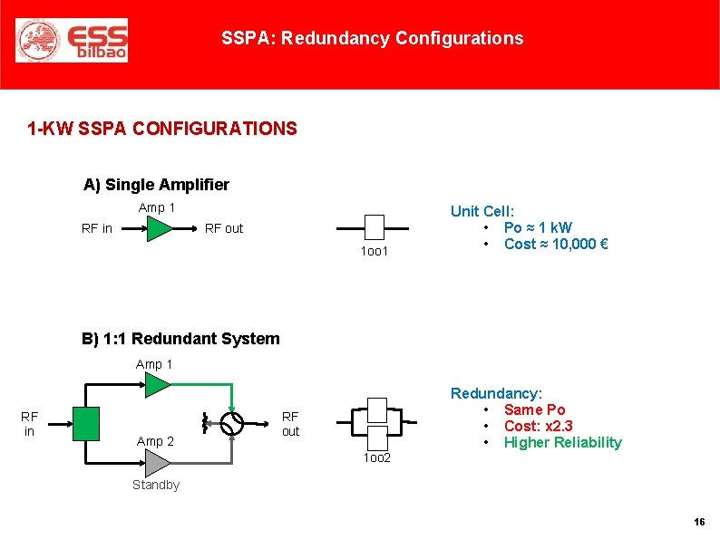
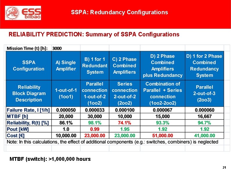
SSPA: Redundancy Configurations 1 -KW SSPA CONFIGURATIONS A) Single Amplifier Amp 1 RF in RF out 1 oo 1 Unit Cell: • Po ≈ 1 k. W • Cost ≈ 10, 000 € B) 1: 1 Redundant System Amp 1 RF in Amp 2 Redundancy: • Same Po • Cost: x 2. 3 • Higher Reliability RF out 1 oo 2 Standby 16

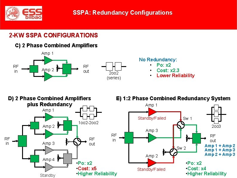
SSPA: Redundancy Configurations 2 -KW SSPA CONFIGURATIONS C) 2 Phase Combined Amplifiers Amp 1 RF in Amp 2 RF out D) 2 Phase Combined Amplifiers plus Redundancy 2 oo 2 (series) No Redundancy: • Po: x 2 • Cost: x 2. 3 • Lower Reliability E) 1: 2 Phase Combined Redundancy System Amp 1 Amp 2 RF in Amp 3 Amp 4 Standby/Failed 1 oo 2 -2 oo 2 Sw 1 2 oo 3 Amp 3 RF out RF in Standby Amp 2 • Po: x 2 • Cost: x 5 • Higher Reliability Standby/Failed Sw 2 RF out Amp 1 + Amp 2 Amp 1 + Amp 3 Amp 2 + Amp 3 • Po: x 2 • Cost: x 4 • Higher Reliability

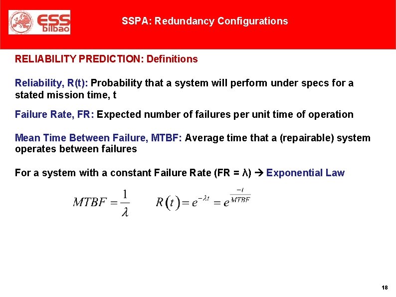
SSPA: Redundancy Configurations RELIABILITY PREDICTION: Definitions Reliability, R(t): Probability that a system will perform under specs for a stated mission time, t Failure Rate, FR: Expected number of failures per unit time of operation Mean Time Between Failure, MTBF: Average time that a (repairable) system operates between failures For a system with a constant Failure Rate (FR = λ) Exponential Law 18

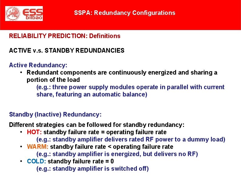
SSPA: Redundancy Configurations RELIABILITY PREDICTION: Definitions ACTIVE v. s. STANDBY REDUNDANCIES Active Redundancy: • Redundant components are continuously energized and sharing a portion of the load (e. g. : three power supply modules operate in parallel with current share, featuring an automatic balance) Standby (Inactive) Redundancy: Different strategies can be followed for standby redundancy: • HOT: standby failure rate = operating failure rate (e. g. : standby amplifier delivers rated RF power to a dummy load) • WARM: standby failure rate < operating failure rate (e. g. : standby amplifier is energized, but delivers no RF) • COLD: standby failure rate = 0 (e. g. : standby amplifier is switched off)

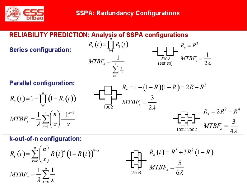
SSPA: Redundancy Configurations RELIABILITY PREDICTION: Analysis of SSPA configurations Series configuration: 2 oo 2 (series) Parallel configuration: 1 oo 2 -2 oo 2 k-out-of-n configuration: 2 oo 3

SSPA: Redundancy Configurations RELIABILITY PREDICTION: Summary of SSPA Configurations MTBF (switch): >1, 000 hours 21

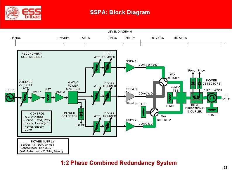
SSPA: Block Diagram LEVEL DIAGRAM -16 d. Bm +12 d. Bm +5 d. Bm REDUNDANCY CONTROL BOX 0 d. Bm +60 d. Bm +62. 7 d. Bm +62. 5 d. Bm PHASE ATT TRIMMER SSPA 1 COAX-WR 340 PFWD PREV WG SWITCH 1 AMP 2 ATT PHASE TRIMMER CONTROL -WG Switches -Pdrive, Pfwd, Prev -Psspa, Tsspa (x 3) -Power Supply -VVAtt MAGIC TEE SSPA 3 COAX-WG Standby LOAD POWER DETECTOR ATT PHASE TRIMMER PDRIVE CIRCULATOR RF OUT LOAD WG SWITCH 2 SSPA 2 POWER DETECTORS R ATT 4 -WAY POWER SPLITTER F RFGEN VOLTAGE VARIABLE ATT AMP 1 DUAL DIRECTIONAL COUPLER LOAD COAX-WG POWER SUPPLY -SSPAs (x 3) (50 V, 7 Amp) -Control box (12 V, 3. 3 V) -WG Switches (x 2) (24 V, 3 Amp) 1: 2 Phase Combined Redundancy System 22

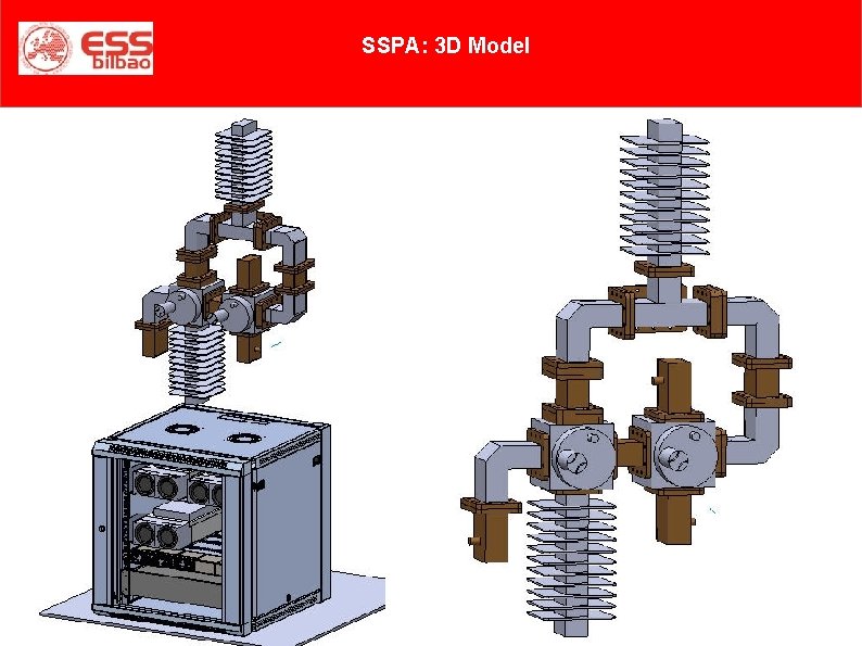
SSPA: 3 D Model

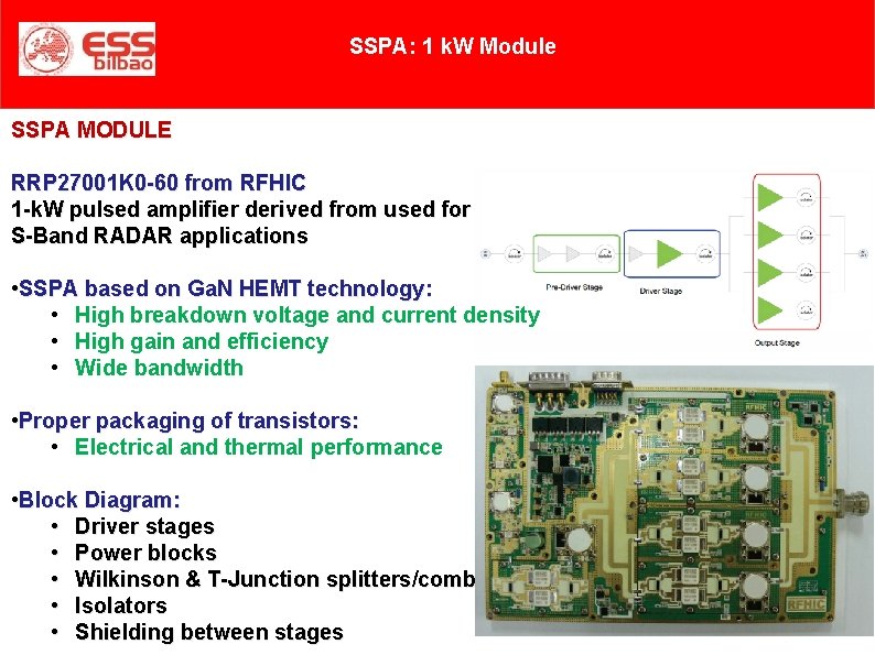
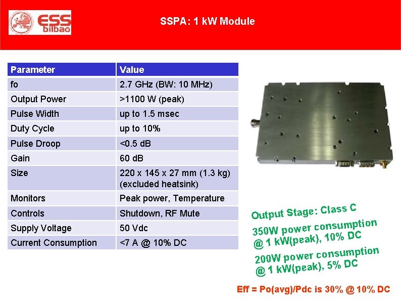
SSPA: 1 k. W Module SSPA MODULE RRP 27001 K 0 -60 from RFHIC 1 -k. W pulsed amplifier derived from used for S-Band RADAR applications • SSPA based on Ga. N HEMT technology: • High breakdown voltage and current density • High gain and efficiency • Wide bandwidth • Proper packaging of transistors: • Electrical and thermal performance • Block Diagram: • Driver stages • Power blocks • Wilkinson & T-Junction splitters/combiners • Isolators • Shielding between stages

SSPA: 1 k. W Module Parameter Value fo 2. 7 GHz (BW: 10 MHz) Output Power >1100 W (peak) Pulse Width up to 1. 5 msec Duty Cycle up to 10% Pulse Droop <0. 5 d. B Gain 60 d. B Size 220 x 145 x 27 mm (1. 3 kg) (excluded heatsink) Monitors Peak power, Temperature Controls Shutdown, RF Mute Supply Voltage 50 Vdc Current Consumption <7 A @ 10% DC lass C C : e g a t S t u p Out ption m u s n o c r e w 350 W po ), 10% DC k a e p ( W k 1 @ mption u s n o c r e w o 200 W p % DC 5 , ) k a e p ( W k @1 Eff = Po(avg)/Pdc is 30% @ 10% DC

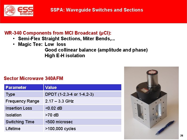
SSPA: Waveguide Switches and Sections WR-340 Components from MCI Broadcast (μCI): • Semi-Flex Straight Sections, Miter Bends, . . . • Magic Tee: Low loss Good collinear balance (amplitude and phase) High E-H isolation Sector Microwave 340 AFM Parameter Value Type DPDT (1 -2, 3 -4 or 1 -4, 2 -3) Frequency Range 2. 17 – 3. 3 GHz Insertion Loss <0. 02 d. B Isolation >70 d. B Switching Time <500 microsec Lifetime >100, 000 cycles 26

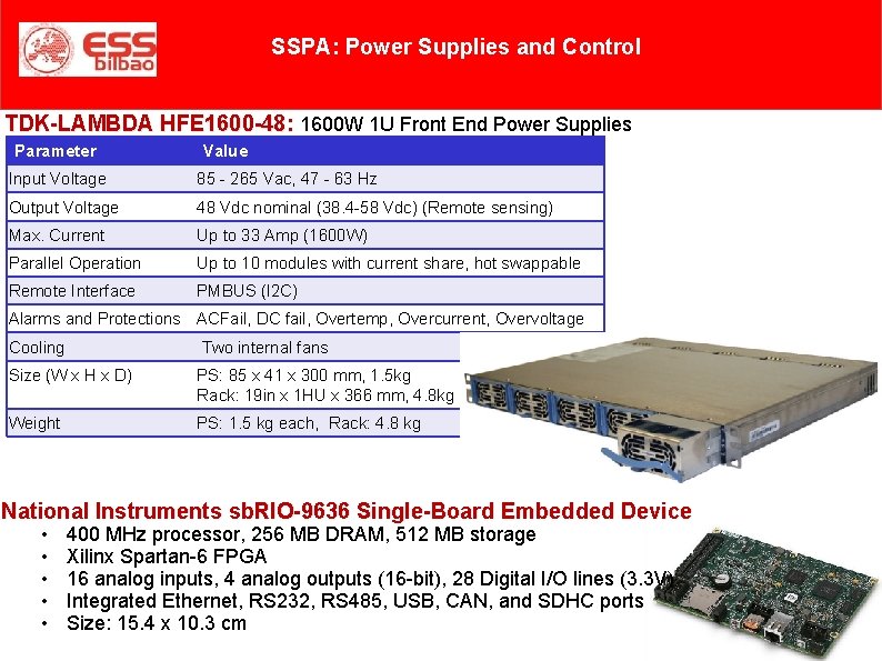
SSPA: Power Supplies and Control TDK-LAMBDA HFE 1600 -48: 1600 W 1 U Front End Power Supplies Parameter Value Input Voltage 85 - 265 Vac, 47 - 63 Hz Output Voltage 48 Vdc nominal (38. 4 -58 Vdc) (Remote sensing) Max. Current Up to 33 Amp (1600 W) Parallel Operation Up to 10 modules with current share, hot swappable Remote Interface PMBUS (I 2 C) Alarms and Protections ACFail, DC fail, Overtemp, Overcurrent, Overvoltage Cooling Two internal fans Size (W x H x D) PS: 85 x 41 x 300 mm, 1. 5 kg Rack: 19 in x 1 HU x 366 mm, 4. 8 kg Weight PS: 1. 5 kg each, Rack: 4. 8 kg National Instruments sb. RIO-9636 Single-Board Embedded Device • • • 400 MHz processor, 256 MB DRAM, 512 MB storage Xilinx Spartan-6 FPGA 16 analog inputs, 4 analog outputs (16 -bit), 28 Digital I/O lines (3. 3 V) Integrated Ethernet, RS 232, RS 485, USB, CAN, and SDHC ports Size: 15. 4 x 10. 3 cm

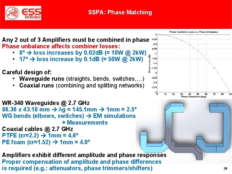
SSPA: Phase Matching Any 2 out of 3 Amplifiers must be combined in phase Phase unbalance affects combiner losses: • 8º loss increases by 0. 02 d. B (≈ 10 W @ 2 k. W) • 17º loss increase by 0. 1 d. B (≈ 50 W @ 2 k. W) Careful design of: • Waveguide runs (straights, bends, switches, …) • Coaxial runs (combining and splitting networks) WR-340 Waveguides @ 2. 7 GHz 86. 36 x 43. 18 mm λg = 145. 1 mm ≈ 2. 5º WG bends (elbows, switches) EM simulations + Measurements Coaxial cables @ 2. 7 GHz PTFE (εr≈2. 2) 1 mm ≈ 4. 6º PE foam (εr≈1. 52) 1 mm ≈ 4. 0º Amplifiers exhibit different amplitude and phase responses Proper compensation of amplitude and phase differences is required (e. g. : attenuators, phase trimmers/shifters) 28

Bibliography • Status of the Ion Sources at ESS-Bilbao, J. Feuchtwanger et al. , IPAC’ 12, New Orleans (USA), 2012. • Automatic Tuner Unit Operation for the Microwave System of the ESS-Bilbao H+ Ion Source, L. Muguira et al. , IPAC’ 12, New Orleans (USA), 2012. • Last results of the continuous-wave high-intensity light ion source at CEA Saclay, R. Gobin et al. , Rev. Sci. Instrum. 69, 1998 • Phase Combined Amplifiers as a Means of Achieving High Output Power and Redundancy (Whitepaper), Stephen D. Turner, Paradise Datacom. • Design for Reliability, D. Crow and A. Feinberg, CRC Press, 2000 • Design for Accelerator Reliability, P. Pierini and D. Sertore, TESLA Meeting, 2003 • 1 k. W S-band Solid State Radar Amplifier, Ju-Young Kwack, Ki-Won Kim, Samuel Cho, IEEE 12 th WAMICON, 2011.

Acknowledgements Thank you very much for your attention! Thanks also to ESS Bilbao ISHP Team: Ion Sources Control Diagnostics Jorge Feuchtwanger* Rosalba Miracoli Slobodan Djekic F. Javier Corres Iñigo Arredondo Mikel Eguiraun Daniel Piso* María del Campo* RF Electrical Accelerating Structures Giles Harper Xabier González Jon Bilbao Gorka Mugika Adolfo Vélez Oscar González Nagore Garmendia Leire Muguira Arash Kaftoosian Tomaso Poggi F. Javier Fernández Jordi Verdú* * No longer at ESS-Bilbao ** University of the Basque Country Daniel Belver Pablo Echevarria Seadat Varnasseri EHU/UPV** Víctor Echevarría Joaquín Portilla Josu Jugo