Design of a Nonvacuumcooling compact scientific CCD camera

- Slides: 1

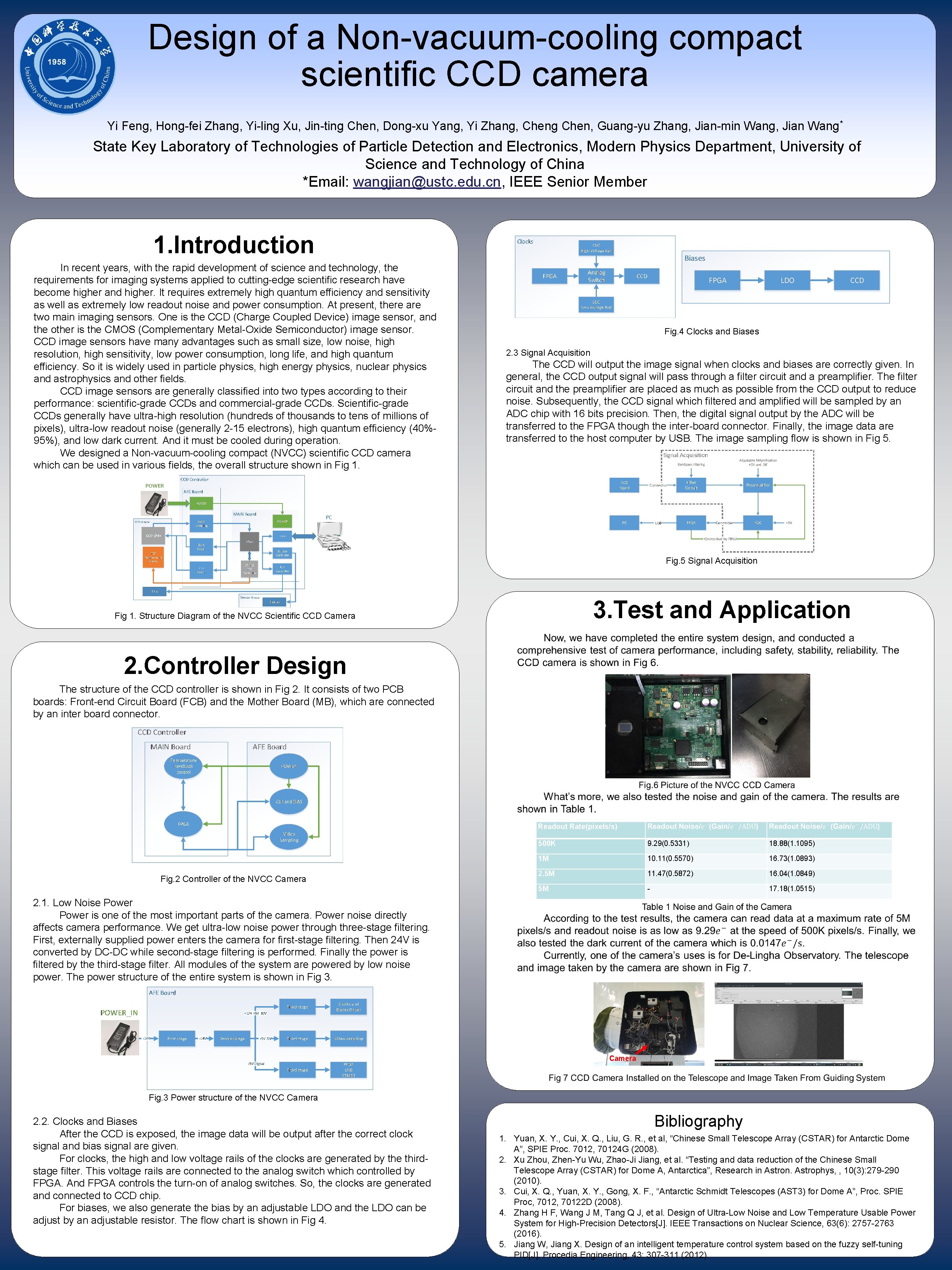
Design of a Non-vacuum-cooling compact scientific CCD camera Yi Feng, Hong-fei Zhang, Yi-ling Xu, Jin-ting Chen, Dong-xu Yang, Yi Zhang, Cheng Chen, Guang-yu Zhang, Jian-min Wang, Jian Wang* State Key Laboratory of Technologies of Particle Detection and Electronics, Modern Physics Department, University of Science and Technology of China *Email: wangjian@ustc. edu. cn, IEEE Senior Member 1. Introduction In recent years, with the rapid development of science and technology, the requirements for imaging systems applied to cutting-edge scientific research have become higher and higher. It requires extremely high quantum efficiency and sensitivity as well as extremely low readout noise and power consumption. At present, there are two main imaging sensors. One is the CCD (Charge Coupled Device) image sensor, and the other is the CMOS (Complementary Metal-Oxide Semiconductor) image sensor. CCD image sensors have many advantages such as small size, low noise, high resolution, high sensitivity, low power consumption, long life, and high quantum efficiency. So it is widely used in particle physics, high energy physics, nuclear physics and astrophysics and other fields. CCD image sensors are generally classified into two types according to their performance: scientific-grade CCDs and commercial-grade CCDs. Scientific-grade CCDs generally have ultra-high resolution (hundreds of thousands to tens of millions of pixels), ultra-low readout noise (generally 2 -15 electrons), high quantum efficiency (40%95%), and low dark current. And it must be cooled during operation. We designed a Non-vacuum-cooling compact (NVCC) scientific CCD camera which can be used in various fields, the overall structure shown in Fig 1. Fig. 4 Clocks and Biases 2. 3 Signal Acquisition The CCD will output the image signal when clocks and biases are correctly given. In general, the CCD output signal will pass through a filter circuit and a preamplifier. The filter circuit and the preamplifier are placed as much as possible from the CCD output to reduce noise. Subsequently, the CCD signal which filtered and amplified will be sampled by an ADC chip with 16 bits precision. Then, the digital signal output by the ADC will be transferred to the FPGA though the inter-board connector. Finally, the image data are transferred to the host computer by USB. The image sampling flow is shown in Fig 5. Fig. 5 Signal Acquisition 3. Test and Application Fig 1. Structure Diagram of the NVCC Scientific CCD Camera 2. Controller Design The structure of the CCD controller is shown in Fig 2. It consists of two PCB boards: Front-end Circuit Board (FCB) and the Mother Board (MB), which are connected by an inter board connector. Readout Rate(pixels/s) Fig. 2 Controller of the NVCC Camera 500 K 9. 29(0. 5331) 18. 88(1. 1095) 1 M 10. 11(0. 5570) 16. 73(1. 0893) 2. 5 M 11. 47(0. 5872) 16. 04(1. 0849) 5 M - 17. 18(1. 0515) 2. 1. Low Noise Power is one of the most important parts of the camera. Power noise directly affects camera performance. We get ultra-low noise power through three-stage filtering. First, externally supplied power enters the camera for first-stage filtering. Then 24 V is converted by DC-DC while second-stage filtering is performed. Finally the power is filtered by the third-stage filter. All modules of the system are powered by low noise power. The power structure of the entire system is shown in Fig 3. Camera Fig. 3 Power structure of the NVCC Camera Bibliography 1. Yuan, X. Y. , Cui, X. Q. , Liu, G. R. , et al, “Chinese Small Telescope Array (CSTAR) for Antarctic Dome A”, SPIE Proc. 7012, 70124 G (2008). 2. Xu Zhou, Zhen-Yu Wu, Zhao-Ji Jiang, et al. “Testing and data reduction of the Chinese Small Telescope Array (CSTAR) for Dome A, Antarctica”, Research in Astron. Astrophys, , 10(3): 279 -290 (2010). 3. Cui, X. Q. , Yuan, X. Y. , Gong, X. F. , “Antarctic Schmidt Telescopes (AST 3) for Dome A”, Proc. SPIE Proc, 70122 D (2008). 4. Zhang H F, Wang J M, Tang Q J, et al. Design of Ultra-Low Noise and Low Temperature Usable Power System for High-Precision Detectors[J]. IEEE Transactions on Nuclear Science, 63(6): 2757 -2763 (2016). 5. Jiang W, Jiang X. Design of an intelligent temperature control system based on the fuzzy self-tuning www. postersession. com PID[J]. Procedia Engineering, 43: 307 -311 (2012). www. postersession. com 2. 2. Clocks and Biases After the CCD is exposed, the image data will be output after the correct clock signal and bias signal are given. For clocks, the high and low voltage rails of the clocks are generated by the thirdstage filter. This voltage rails are connected to the analog switch which controlled by FPGA. And FPGA controls the turn-on of analog switches. So, the clocks are generated and connected to CCD chip. For biases, we also generate the bias by an adjustable LDO and the LDO can be adjust by an adjustable resistor. The flow chart is shown in Fig 4.