Design of a 16 bit DAC for ECAL
Design of a 16 bit DAC for ECAL calibration Status report D. Dzahini, L. Gallin-Martel, O. Rossetto, C. Vescovi Laboratoire de Physique Subatomique et de Cosmologie, Grenoble • • • Theory – modulators – 1 st order modulator implementation Design – Modulator – Dynamic Element Matching – SC DAC – SC Filter Conclusion – Remaining tasks Calice Meeting – Prague September 12 th 2007 1
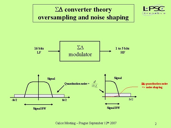
converter theory oversampling and noise shaping modulator 16 bits LF 1 to 5 bits HF Signal quantization noise => noise shaping Quantization noise = -fe/2 Signal BW Calice Meeting – Prague September 12 th 2007 2
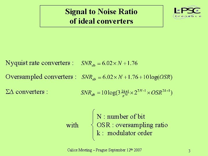
Signal to Noise Ratio of ideal converters Nyquist rate converters : Oversampled converters : with N : number of bit OSR : oversampling ratio k : modulator order Calice Meeting – Prague September 12 th 2007 3
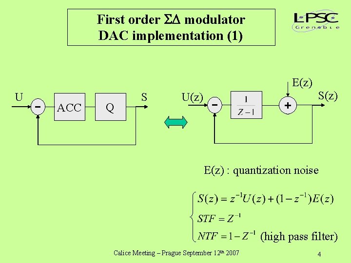
First order modulator DAC implementation (1) E(z) U ACC Q S S(z) U(z) E(z) : quantization noise (high pass filter) Calice Meeting – Prague September 12 th 2007 4
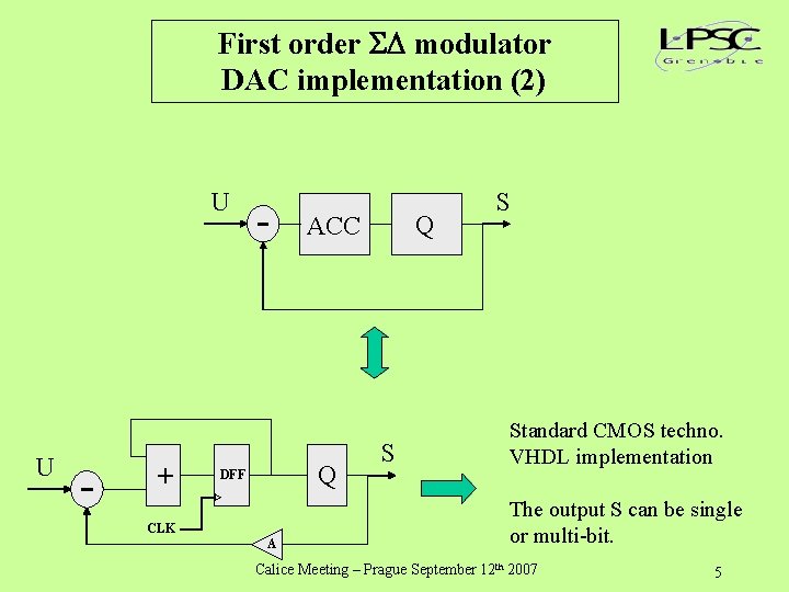
First order modulator DAC implementation (2) U U + Q ACC Q DFF CLK A S S Standard CMOS techno. VHDL implementation The output S can be single or multi-bit. Calice Meeting – Prague September 12 th 2007 5

A 16 bit DAC block diagram From pulser Offset cancelation 16 bits 3 rd order 9 level modulator 9 level DEM 9 level SC DAC 4 th order SC filter Diff to Single CT filter Single ended output voltage CLK Calice Meeting – Prague September 12 th 2007 6

A 16 bit DAC 3 rd order, 9 level modulator (1) A 96 d. B SNR is necessary to achieve a 16 bit resolution. A 3 rd order, 9 level (3. 2 bit) modulator leads to a SNR : 168 d. B for OSR=256 147 d. B for OSR=128 126 d. B for OSR=64 => related to the SC filter design (settling time). Multi-bit : SC filtering and OPA constraints are relaxed quantization noise is reduced, a DEM is necessary to reduce the DNL effect of the 9 level DAC. The modulator was designed using the Matlab toolbox written by R. Schreier Calice Meeting – Prague September 12 th 2007 7

A 16 bit DAC 3 rd order, 9 level modulator (2) b 1 + U 16 bits Z-1 x 1 c 1 + Z-1 x 2 c 2 + a 2 a 1 x 3 Z-1 a 3 c 3 Q S 4 bits (3. 2) VHDL implementation Can also be simulated using C language S=c 3*x 3; if (S>4) S=4; if (S<-4) S=-4; x 3=x 3 + c 2*x 2 - a 3*S; x 2=x 2 + c 1*x 1 - a 2*S; x 1=x 1 + U - a 1*S; Calice Meeting – Prague September 12 th 2007 Adders overflow is not simulated with this code. 8
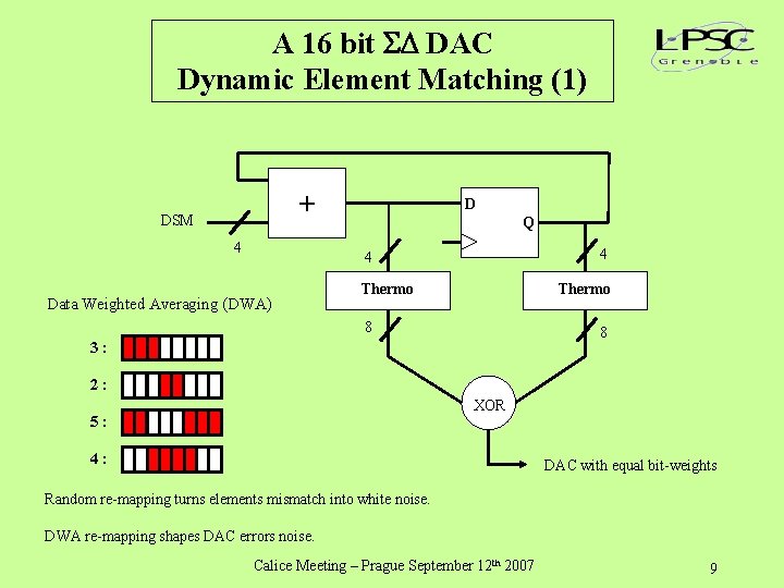
A 16 bit DAC Dynamic Element Matching (1) + DSM 4 D Q 4 4 Data Weighted Averaging (DWA) Thermo 8 8 3: 2: XOR 5: 4: DAC with equal bit-weights Random re-mapping turns elements mismatch into white noise. DWA re-mapping shapes DAC errors noise. Calice Meeting – Prague September 12 th 2007 9

A 16 bit DAC Dynamic Element Matching (2) Calice Meeting – Prague September 12 th 2007 10
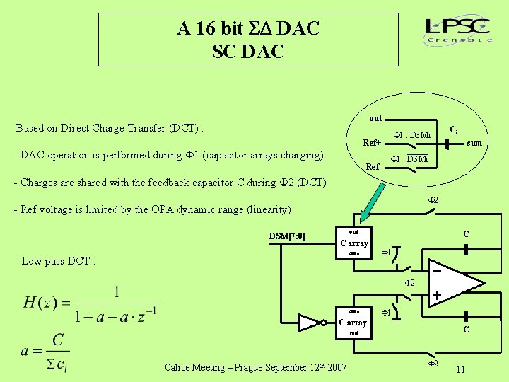
A 16 bit DAC SC DAC out Based on Direct Charge Transfer (DCT) : 1. DSMi Ref+ - DAC operation is performed during 1 (capacitor arrays charging) Ref- Ci sum 1. DSMi - Charges are shared with the feedback capacitor C during 2 (DCT) 2 - Ref voltage is limited by the OPA dynamic range (linearity) DSM[7: 0] out C array sum Low pass DCT : C 1 2 sum 1 C array C out Calice Meeting – Prague September 12 th 2007 2 11
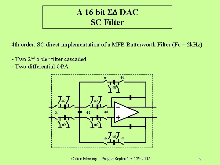
A 16 bit DAC SC Filter 4 th order, SC direct implementation of a MFB Butterworth Filter (Fc = 2 k. Hz) - Two 2 nd order filter cascaded - Two differential OPA 1 1 2 2 1 1 2 2 1 Calice Meeting – Prague September 12 th 2007 12
A 16 bit DAC Differential OPA (1) The OPA used in the SC DAC and in the SC Filter was designed (D. Dzahini) to be implemented in 12 bit , 25 MHz ADCs. The main features of this OPA are : - Open loop gain : - Gain-band product : - Dynamic range : - Power consumption : 100 d. B 130 MHz 1. 6 V 6 m. W (3 instances required => 18 m. W) Simulations have to be carried out to reduce the power consumption. Calice Meeting – Prague September 12 th 2007 13
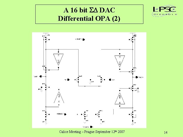
A 16 bit DAC Differential OPA (2) Calice Meeting – Prague September 12 th 2007 14
A 16 bit DAC Remaining tasks - Simulations have to be carried out to complete the SC filter design : filter topology & response OPA power consumption - The output stage has to be designed : differential to single ended converter (if implemented in the 1 st proto) CT filter (if implemented in the 1 st proto) output buffer (s) - Pulser & Offset cancellation : ? Pulser specification and design (who ? ) The modulator has an offset cancellation capability, its control depends on the pulser design. A first prototype will be submitted to the January 2008 run Calice Meeting – Prague September 12 th 2007 15
- Slides: 15