Design Fabrication and Characterization of Ga N High
Design, Fabrication, and Characterization of Ga. N High Power Rectifiers Ph. D. Dissertation Defense Kwang H. Baik Materials Science and Engineering, Univ. of Florida, Gainesville, FL November 2, 2004
Outline q Motivation q Theoretical Calculations § Ga. N Materials Parameters § Intrinsic carrier concentration § Breakdown Voltage (VB) § On-state Resistance (RON) § Forward Voltage Drop (VF) & Leakage Current (IR) q Device Modeling § Breakdown Study with Edge Termination Techniques § Electrical Characteristics of Ga. N Rectifiers q Experimental Data § Ga. N High Voltage Diodes with Field Plate Termination § High Power Schottky Diode Array (Ga. N & Si. C)
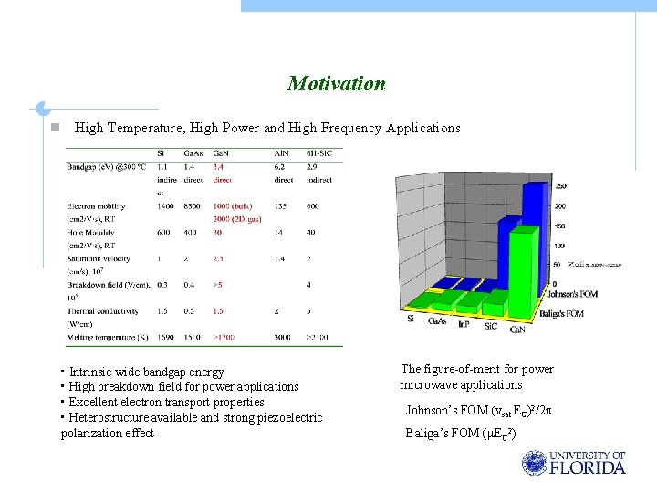
Motivation n High Temperature, High Power and High Frequency Applications • Intrinsic wide bandgap energy • High breakdown field for power applications • Excellent electron transport properties • Heterostructure available and strong piezoelectric polarization effect The figure-of-merit for power microwave applications Johnson’s FOM (vsat EC)2/2 Baliga’s FOM ( EC 2)
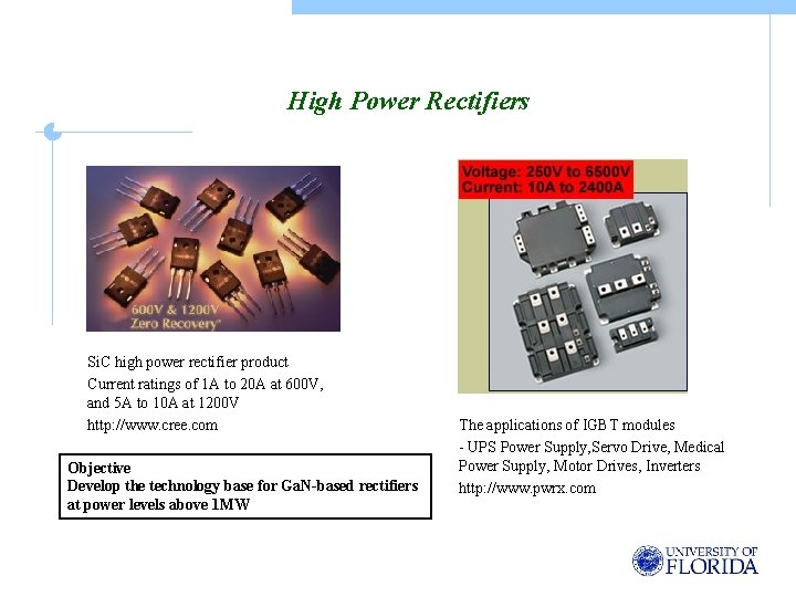
High Power Rectifiers Si. C high power rectifier product Current ratings of 1 A to 20 A at 600 V, and 5 A to 10 A at 1200 V http: //www. cree. com Objective Develop the technology base for Ga. N-based rectifiers at power levels above 1 MW The applications of IGBT modules - UPS Power Supply, Servo Drive, Medical Power Supply, Motor Drives, Inverters http: //www. pwrx. com
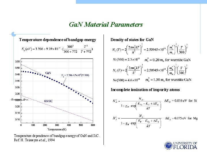
Ga. N Material Parameters Temperature dependence of bandgap energy Density of states for Ga. N Incomplete ionization of impurity atoms Temperature dependence of bandgap energy of Ga. N and Si. C. Ref. H. Teisseyre et al. , 1994
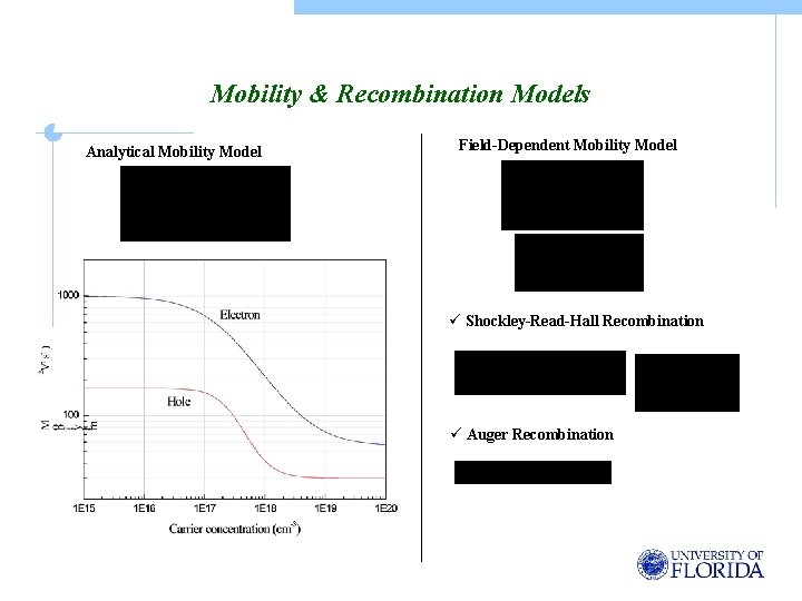
Mobility & Recombination Models Analytical Mobility Model Field-Dependent Mobility Model ü Shockley-Read-Hall Recombination ü Auger Recombination
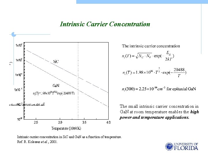
Intrinsic Carrier Concentration The small intrinsic carrier concentration in Ga. N at room temperature enables the high power and temperature applications. Intrinsic carrier concentration in Si. C and Ga. N as a function of temperature. Ref. R. Kolessar et al. , 2001.
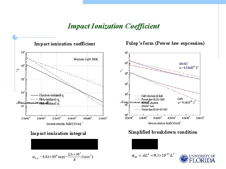
Impact Ionization Coefficient Impact ionization coefficient Impact ionization integral Fulop’s form (Power law expression) Simplified breakdown condition
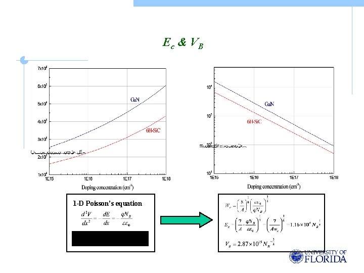
Ec & V B 1 -D Poisson’s equation
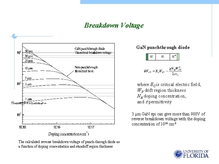
Breakdown Voltage Ga. N punchthrough diode n- n n+ where EC is critical electric field, WP drift region thickness NA doping concentration, and permittivity 3 µm Ga. N epi can give more than 900 V of reverse breakdown voltage with the doping concentration of 1016 cm-3 The calculated reverse breakdown voltage of punch-through diode as a function of doping concentration and standoff region thickness
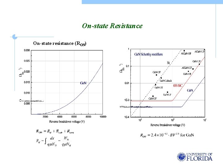
On-state Resistance On-state resistance (RON)
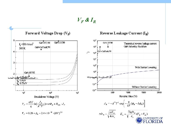
VF & IR Forward Voltage Drop (VF) Reverse Leakage Current (IR)
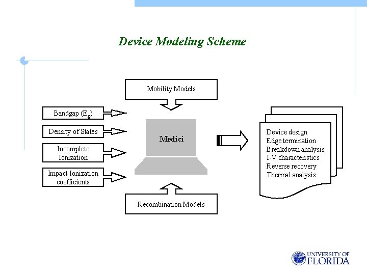
Device Modeling Scheme Mobility Models Bandgap (Eg) Density of States Medici Incomplete Ionization Impact Ionization coefficients Recombination Models Device design Edge termination Breakdown analysis I-V characteristics Reverse recovery Thermal analysis
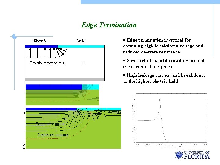
Edge Termination Electrode Depletion region contour Oxide n § Edge termination is critical for obtaining high breakdown voltage and reduced on-state resistance. § Severe electric field crowding around metal contact periphery. § High leakage current and breakdown at the highest electric field Potential contour Depletion contour
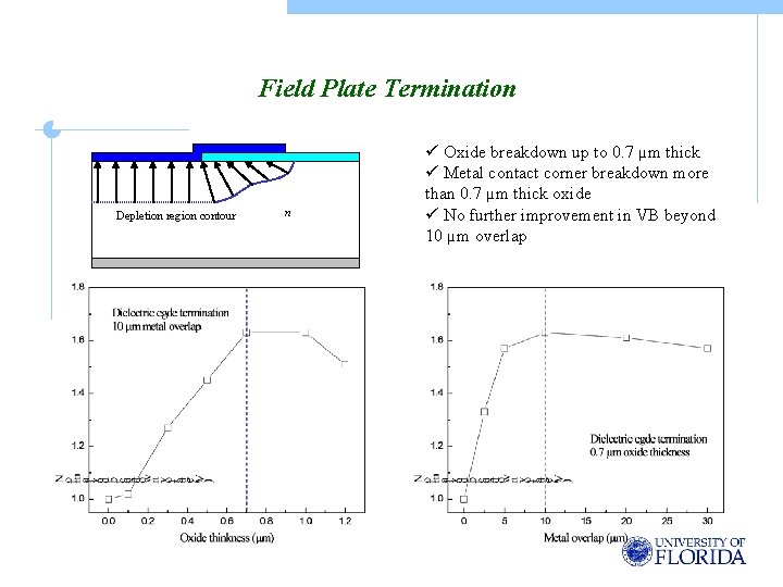
Field Plate Termination Depletion region contour n ü Oxide breakdown up to 0. 7 µm thick ü Metal contact corner breakdown more than 0. 7 µm thick oxide ü No further improvement in VB beyond 10 µm overlap
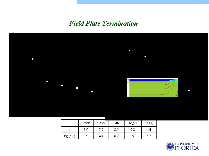
Field Plate Termination Oxide Nitride Al. N Mg. O Sc 2 O 3 3. 9 7. 5 8. 5 9. 8 14 Eg (e. V) 9 4. 7 6. 2 8 6. 3
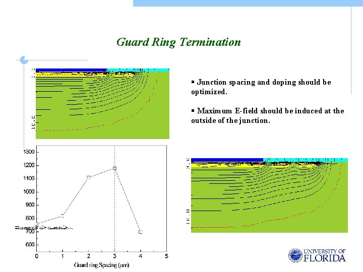
Guard Ring Termination § Junction spacing and doping should be optimized. § Maximum E-field should be induced at the outside of the junction.
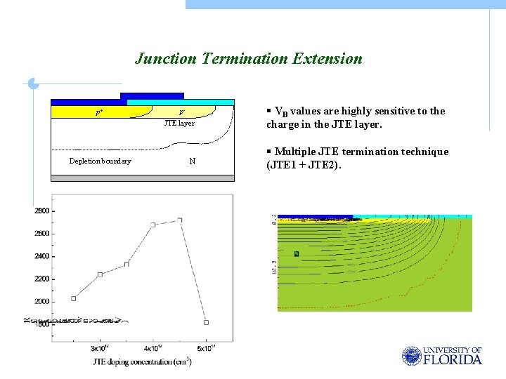
Junction Termination Extension p+ Depletion boundary p. JTE layer N § VB values are highly sensitive to the charge in the JTE layer. § Multiple JTE termination technique (JTE 1 + JTE 2).
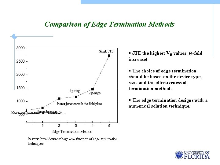
Comparison of Edge Termination Methods § JTE the highest VB values. (4 -fold increase) § The choice of edge termination should be based on the device type, size, and the effectiveness of termination method. § The edge termination designs with a numerical solution technique. Reverse breakdown voltage as a function of edge termination techniques.
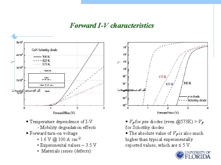
Forward I-V characteristics Anode (Pt) 5 µm n (1 1016 cm-3) 1 µm n+ (5 1019 cm-3) Cathode § Temperature dependence of I-V - Mobility degradation effects § Forward turn-on voltage ▫ 1. 6 V @ 100 A·cm-2 ▫ Experimental values ~ 3. 5 V ▫ Materials issues (defects) § VF for pin diodes (even @573 K) > VF for Schottky diodes § The absolute value of VF is also much higher than typical experimentally reported values, which are 5 V.
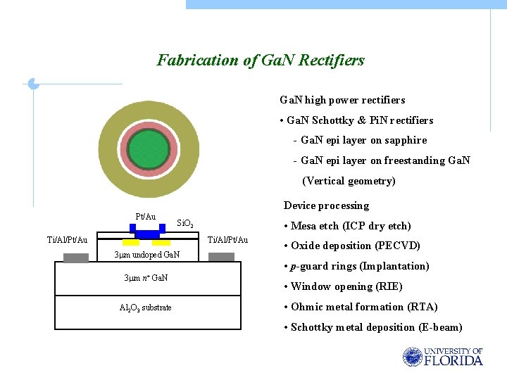
Fabrication of Ga. N Rectifiers Ga. N high power rectifiers • Ga. N Schottky & Pi. N rectifiers - Ga. N epi layer on sapphire - Ga. N epi layer on freestanding Ga. N (Vertical geometry) Device processing Pt/Au Si. O 2 Ti/Al/Pt/Au • Mesa etch (ICP dry etch) Ti/Al/Pt/Au 3 m undoped Ga. N • Oxide deposition (PECVD) • p-guard rings (Implantation) 3 m n+ Ga. N Al 2 O 3 substrate • Window opening (RIE) • Ohmic metal formation (RTA) • Schottky metal deposition (E-beam)
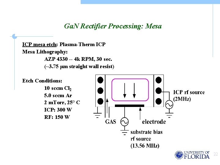
Ga. N Rectifier Processing: Mesa ICP mesa etch: Plasma-Therm ICP Mesa Lithography: AZP 4330 -- 4 k RPM, 30 sec. (~3. 75 µm straight wall resist) Etch Conditions: 10 sccm Cl 2 5. 0 sccm Ar 2 m. Torr, 25° C ICP: 300 W RF: 150 W 22
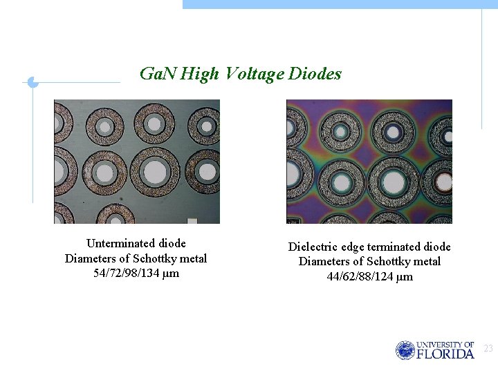
Ga. N High Voltage Diodes Unterminated diode Diameters of Schottky metal 54/72/98/134 µm Dielectric edge terminated diode Diameters of Schottky metal 44/62/88/124 µm 23
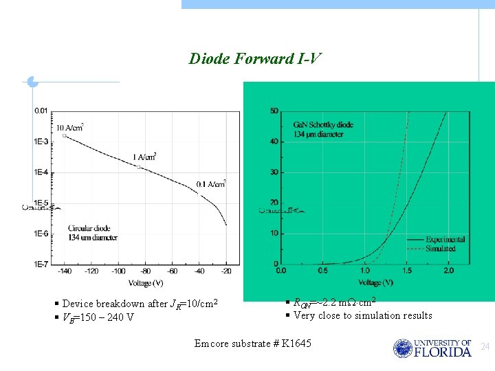
Diode Forward I-V § Device breakdown after JR=10/cm 2 § VB=150 – 240 V § RON=~2. 2 m cm 2 § Very close to simulation results Emcore substrate # K 1645 24
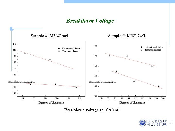
Breakdown Voltage Sample #: M 5221 sc 4 Sample #: M 5217 sc 3 Breakdown voltage at 10 A/cm 2 25
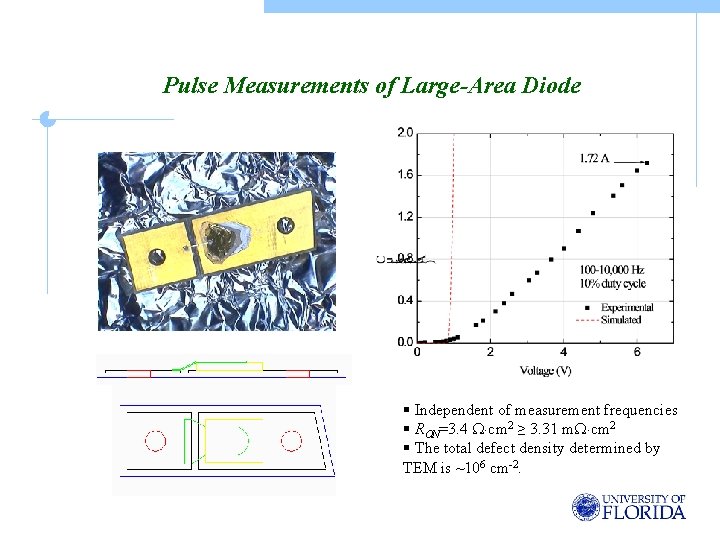
Pulse Measurements of Large-Area Diode § Independent of measurement frequencies § RON=3. 4 cm 2 ≥ 3. 31 m cm 2 § The total defect density determined by TEM is ~106 cm-2.
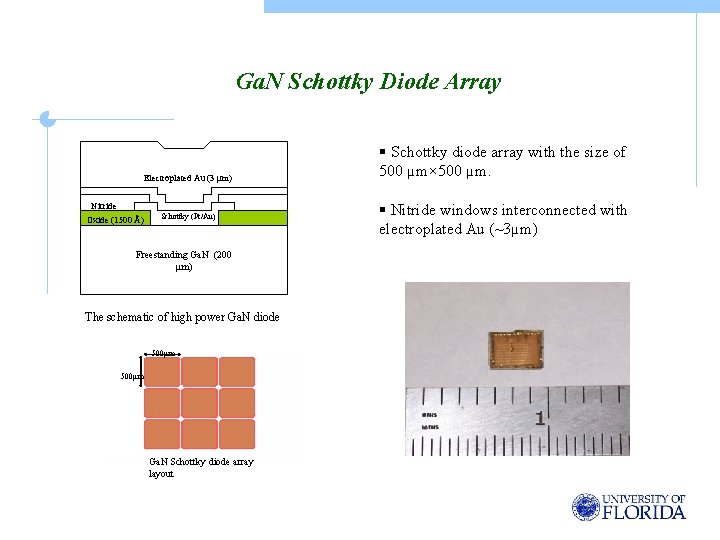
Ga. N Schottky Diode Array Electroplated Au (3 µm) Nitride Oxide (1500 Å) Schottky (Pt/Au) Freestanding Ga. N (200 µm) The schematic of high power Ga. N diode 500µm m 500 500µm Ga. N Schottky diode array layout § Schottky diode array with the size of 500 µm× 500 µm. § Nitride windows interconnected with electroplated Au (~3µm)
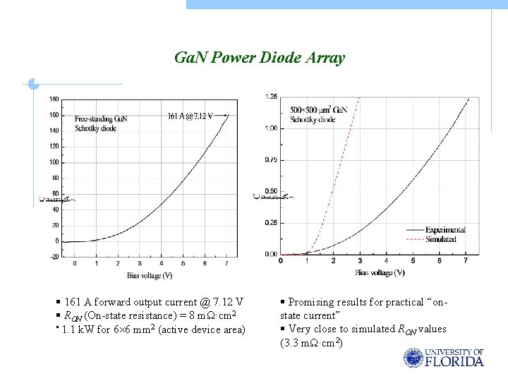
Ga. N Power Diode Array § 161 A forward output current @ 7. 12 V § RON (On-state resistance) = 8 mΩ·cm 2 § 1. 1 k. W for 6 6 mm 2 (active device area) § Promising results for practical “onstate current” § Very close to simulated RON values (3. 3 mΩ·cm 2)
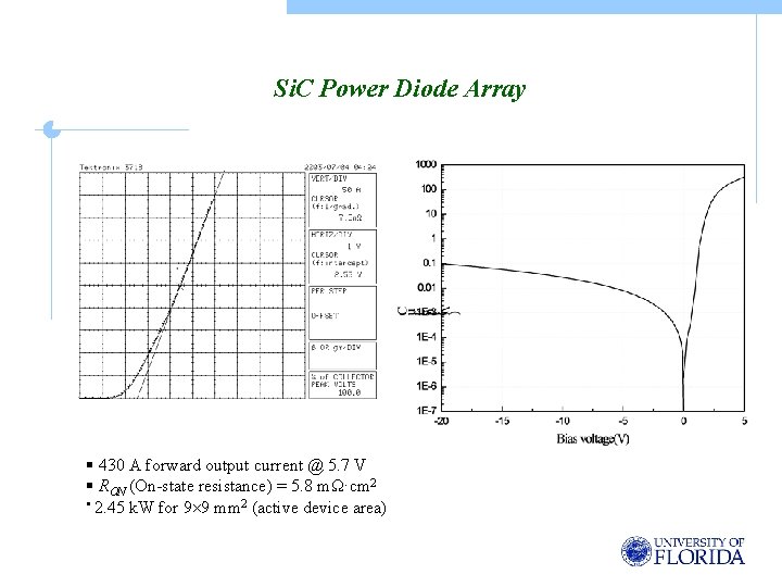
Si. C Power Diode Array § 430 A forward output current @ 5. 7 V § RON (On-state resistance) = 5. 8 mΩ·cm 2 § 2. 45 k. W for 9 9 mm 2 (active device area)
Acknowledgement § Y. Irokawa, J. R. La. Roche, B. S. Kang, J. Kim, and K. P. Lee § Professors F. Ren and S. J. Pearton § S. S. Park and S. K. Lee for Ga. N substrates § D. Sheridan and G. Y. Chung about device modeling
- Slides: 30