Design Examples Using VHDL UNITIV TOPICS COVERED Barrel
 UNIT-IV")
Design Examples (Using VHDL) UNIT-IV

TOPICS COVERED • • Barrel Shifter Comparators Floating-point encoder dual parity encoder

VHDL behavioral description of a 6 -function barrel shifter: use IEEE. std_logic_1164. all; use IEEE. std_logic_arith. all; entity barrel 16 is port ( DIN: in STD_LOGIC_VECTOR (15 downto 0); -Data inputs S: in UNSIGNED (3 downto 0); -- Shift amount, 015 C: in STD_LOGIC_VECTOR (2 downto 0); -- Mode control DOUT: out STD_LOGIC_VECTOR (15 downto 0) -Data bus output); constant Lrotate: STD_LOGIC_VECTOR : = "000"; - Define the coding of constant Rrotate: STD_LOGIC_VECTOR : = "001"; -- different shift modes constant Llogical: STD_LOGIC_VECTOR : = "010"; constant Rlogical: STD_LOGIC_VECTOR : = "011"; constant Larith: STD_LOGIC_VECTOR : = "100"; constant Rarith: STD_LOGIC_VECTOR : = "101"; end barrel 16; architecture barrel 16_behavioral of barrel 16 is subtype DATAWORD is STD_LOGIC_VECTOR(15 downto 0); function Vrol (D: DATAWORD; S: UNSIGNED) return DATAWORD is variable N: INTEGER; variable TMPD: DATAWORD; begin N : = CONV_INTEGER(S); TMPD : = D; for i in 1 to N loop TMPD : = TMPD(14 downto 0) & TMPD(15); end loop; return TMPD; end Vrol; . . . begin process(DIN, S, C) begin case C is when Lrotate => DOUT <= Vrol(DIN, S); when Rrotate => DOUT <= Vror(DIN, S); when Illogical => DOUT <= Vsll(DIN, S); when Rlogical => DOUT <= Vsrl(DIN, S); when Larith => DOUT <= Vsla(DIN, S); when Rarith => DOUT <= Vsra(DIN, S); when others => DOUT <= DIN; end case; end process; end barrel 16_behavioral;

VHDL program for a 16 -bit barrel shifter for left circular shifts only: library IEEE; use IEEE. std_logic_1164. all; entity rol 16 is port ( DIN: in STD_LOGIC_VECTOR(15 downto 0); -- Data inputs S: in STD_LOGIC_VECTOR (3 downto 0); -- Shift amount, 0 -15 DOUT: out STD_LOGIC_VECTOR(15 downto 0) -- Data bus output); end rol 16; architecture rol 16_arch of rol 16 is begin process(DIN, S) variable X, Y, Z: STD_LOGIC_VECTOR(15 downto 0); begin if S(0)='1' then X : = DIN(14 downto 0) & DIN(15); else X : = DIN; end if; if S(1)='1' then Y : = X(13 downto 0) & X(15 downto 14); else Y : = X; end if; if S(2)='1' then Z : = Y(11 downto 0) & Y(15 downto 12); else Z : = Y; end if; if S(3)='1' then DOUT <= Z(7 downto 0) & Z(15 downto 8); else DOUT <= Z; end if; end process; end rol 16_arch;

VHDL program for an 8 -bit comparator: library IEEE; use IEEE. std_logic_1164. all; use IEEE. std_logic_unsigned. all; entity comp 8 is port ( A, B: in STD_LOGIC_VECTOR (7 downto 0); EQ, GT: out STD_LOGIC ); end comp 8; architecture comp 8_arch of comp 8 is begin EQ <= '1' when A = B else '0'; GT <= '1' when A > B else '0'; end comp 8_arch;

Behavioral VHDL program for fixed-point to floating-point conversion: library IEEE; use IEEE. std_logic_1164. all; use IEEE. std_logic_arith. all; entity fpenc is port (B: in STD_LOGIC_VECTOR(10 downto 0); -- fixed-point number M: out STD_LOGIC_VECTOR(3 downto 0); -- floating-point mantissa E: out STD_LOGIC_VECTOR(2 downto 0) -- floating-point exponent); end fpenc; architecture fpenc_arch of fpenc is begin process(B) variable BU: UNSIGNED(10 downto 0); begin BU : = UNSIGNED(B); if BU < 16 then M <= B( 3 downto 0); E <= "000"; elsif BU < 32 then M <= B( 4 downto 1); E <= "001"; elsif BU < 64 then M <= B( 5 downto 2); E <= "010"; elsif BU < 128 then M <= B( 6 downto 3); E <= "011"; elsif BU < 256 then M <= B( 7 downto 4); E <= "100"; elsif BU < 512 then M <= B( 8 downto 5); E <= "101"; elsif BU < 1024 then M <= B( 9 downto 6); E <= "110"; else M <= B(10 downto 7); E <= "111"; end if; end process; end fpenc_arch;

Alternative VHDL architecture for fixed-point to floating-point conversion: architecture fpence_arch of fpenc is begin process(B) begin if B(10) = '1' then M <= B(10 downto 7); E <= "111"; elsif B(9) = '1' then M <= B( 9 downto 6); E <= "110"; elsif B(8) = '1' then M <= B( 8 downto 5); E <= "101"; elsif B(7) = '1' then M <= B( 7 downto 4); E <= "100"; elsif B(6) = '1' then M <= B( 6 downto 3); E <= "011"; elsif B(5) = '1' then M <= B( 5 downto 2); E <= "010"; elsif B(4) = '1' then M <= B( 4 downto 1); E <= "001"; else M <= B( 3 downto 0); E <= "000"; end if; end process; end fpence_arch;

dual-priority encoder: library IEEE; use IEEE. std_logic_1164. all; use IEEE. std_logic_arith. all; entity Vprior 2 is port ( R: in STD_LOGIC_VECTOR (0 to 7); A, B: out STD_LOGIC_VECTOR (2 downto 0); AVALID, BVALID: buffer STD_LOGIC ); end Vprior 2; architecture Vprior 2_arch of Vprior 2 is begin process(R, AVALID, BVALID) begin AVALID <= '0'; BVALID <= '0'; A <= "000"; B <= "000"; for i in 0 to 7 loop if R(i) = '1' and AVALID = '0' then A <= CONV_STD_LOGIC_VECTOR(i, 3); AVALID <= '1'; elsif R(i) = '1' and BVALID = '0' then B <= CONV_STD_LOGIC_VECTOR(i, 3); BVALID <= '1'; end if; end loop; end process; end Vprior 2_arch;

Alternative VHDL architecture for a dual-priority encoder: architecture Vprior 2 i_arch of Vprior 2 is begin process(R, A, AVALID, BVALID) begin if R(0) = '1' then A <= "000"; AVALID <= '1'; elsif R(1) = '1' then A <= "001"; AVALID <= '1'; elsif R(2) = '1' then A <= "010"; AVALID <= '1'; elsif R(3) = '1' then A <= "011"; AVALID <= '1'; elsif R(4) = '1' then A <= "100"; AVALID <= '1'; elsif R(5) = '1' then A <= "101"; AVALID <= '1'; elsif R(6) = '1' then A <= "110"; AVALID <= '1'; elsif R(7) = '1' then A <= "111"; AVALID <= '1'; else A <= "000"; AVALID <= '0'; end if; if R(1) = '1' and A /= "001" then B <= "001"; BVALID <= '1'; elsif R(2) = '1' and A /= "010" then B <= "010"; BVALID <= '1'; elsif R(3) = '1' and A /= "011" then B <= "011"; BVALID <= '1'; elsif R(4) = '1' and A /= "100" then B <= "100"; BVALID <= '1'; elsif R(5) = '1' and A /= "101" then B <= "101"; BVALID <= '1'; elsif R(6) = '1' and A /= "110" then B <= "110"; BVALID <= '1'; elsif R(7) = '1' and A /= "111" then B <= "111"; BVALID <= '1'; else B <= "000"; BVALID <= '0'; end if; end process; end Vprior 2 i_arch;

SEQUENTIAL LOGIC DESIGN

Difference between combinational and sequential logic circuits A combinational logic circuit is one whose outputs depend only on its current inputs. A sequential logic circuit is one whose outputs depend not only on its current inputs, but also on the past sequence of inputs, possibly arbitrarily far back in time. Eg: The rotary channel selector knob on an old-fashioned TV is like a combinational circuit—its “output” selects a channel based only on its current “input”—the position of the knob. Eg: The circuit controlled by the channel-up and channeldown pushbuttons on a TV or VCR is a sequential circuit—the channel selection depends on the past sequence of up/down pushes, at least since when you started viewing 10 hours before, and perhaps as far back as when you first plugged the device into the wall. It is convenient to describe the behavior of a sequential circuit by means of a table that lists outputs as a function of the input sequence. It is inconvenient, and often impossible, to describe the behavior of a sequential circuit by means of a table that lists outputs as a function of the input sequence that has been received up until the current time.

Clock signals

Metastable behavior

Contd. , • random noise will tend to drive a circuit that is operating at the metastable point toward one of the stable operating points • assume that a small amount of circuit noise reduces Vin 1 by a tiny amount. This causes Vout 1 to increase by a small amount. • But since Vout 1 produces Vin 2, we can follow the first horizontal arrow from near the metastable point to the second transfer characteristic, which now demands a lower voltage for Vout 2, which is Vin 1. • Now we’re back where we started, except we have a much larger change in voltage at Vin 1 than the original noise produced, and the operating point is still changing.

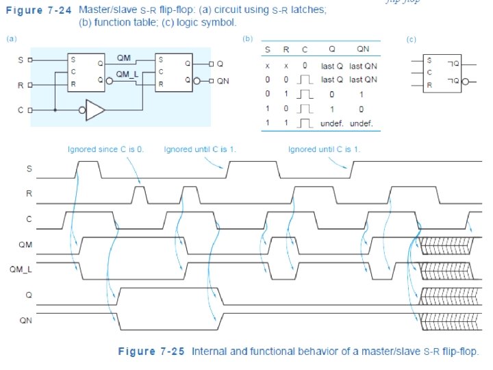
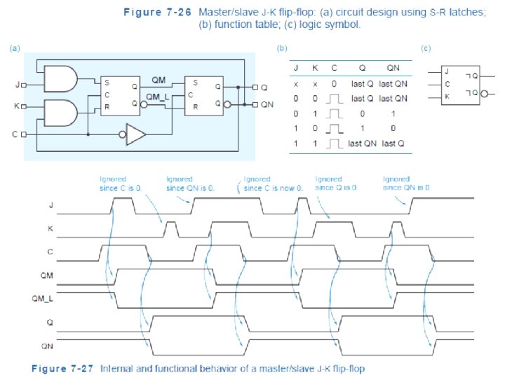
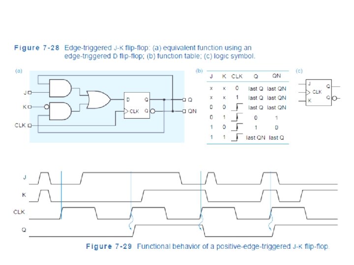
Latches and Flip-Flops Latches Flip-Flops Latch is a device which is used as switch Flip-flop is a storing element They are sensitive to the duration of pulse and can transfer data until they are switched on. They hold the last logic at the output if we put it off(bring the strobe pin to low). They are sensitive to signal change(low to high or high to low) and not the level. Hence they transfer data only at that instant and it cannot be changed until next signal change. They are used as temporary buffers. They are used as registers Latch works without clock signal, but works with a control signal and it is level triggered device. Flip flop is a 1 bit storage element and works with a clock signal. its a edge triggered device. Latches are avoided. Flip flops are preferred. Latch is an asynchronous device and does not need to be synchronized with a clock input. It may have an enable (low or high) and the latch will store the input to the latch when the enable is in its active state. Flip-flop is synchronous and will change states in synch with a clock on either the low-high edge or high-low edge of the clock, depending if the flip-flop is positive or negative edge triggered. By level sensitive we mean that output will respond to change in input as long as the control signal is high. Control signal can be a clock in case of flip flop or any other asynchronous signal in case of latch. By edge sensitive we mean that output will only respond to input at the point when the control signal goes to high from low. Now when the control signal is high the output will not change with change in input. It will again change at the next rising edge of the clock.

Basic SR latch

SR latch with enable

Contd. ,

D latch

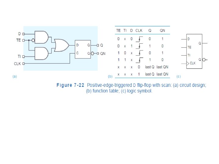
Positive edge triggered D Flip-Flop

Negative edge triggered D Flip-Flop

Positive edge triggered D flip-Flop – IC 74 LS 74

Scan Flip-Flop

PLDs
. A PLA is")
Combinational PLDs • The first PLDs were programmable logic arrays (PLAs). A PLA is a combinational, two-level AND-OR device that can be programmed to realize any sum-of-products logic expression, subject to the size limitations of the device. Limitations are • the number of inputs (n), • the number of outputs (m), and • the number of product terms (p). • • • We might describe such a device as “an n ´ m PLA with p product terms. ” In general, p is far less than the number of n-variable minterms (2 n). Thus, a PLA cannot perform arbitrary n-input, moutput logic functions; its usefulness is limited to functions that can be expressed in sum-ofproducts form using p or fewer product terms. An n ´ m PLA with p product terms contains p 2 n-input AND gates and m p-input OR gates. Figure 521 shows a small PLA with four inputs, six AND gates, and three OR gates and outputs. Each input is connected to a buffer that produces both a true and a complemented version of the signal for use within the array. Potential connections in the array are indicated by X’s; the device is programmed by establishing only the connections that are actually needed. The needed connections are made by fuses, which are actual fusible links or nonvolatile memory cells, depending on technology as we explain in Sections 5. 3. 4 and 5. 3. 5. Thus, each AND gate’s inputs can be any subset of the primary input signals and their complements. Similarly, each OR gate’s inputs can be any subset of the ANDgate outputs. As shown in Figure 5 -22, a more compact diagram can be used to represent a PLA. Moreover, the layout of this diagram more closely resembles the actual internal layout of a PLA chip (e. g. , Figure 5 -28 on page 308).

Combinational PLDs • An n ´ m PLA with p product terms contains p 2 n-input AND gates and m pinput OR gates. Figure 5 -21 shows a small PLA with four inputs, six AND gates, and three OR gates and outputs. Each input is connected to a buffer that produces both a true and a complemented version of the signal for use within the array. Potential connections in the array are indicated by X’s; the device is programmed by establishing only the connections that are actually needed. The needed connections are made by fuses, which are actual fusible links or nonvolatile memory cells, depending on technology as we explain in Sections 5. 3. 4 and 5. 3. 5. Thus, each AND gate’s inputs can be any subset of the primary input signals and their complements. Similarly, each OR gate’s inputs can be any subset of the AND-gate outputs. • As shown in Figure 5 -22, a more compact diagram can be used to represent a PLA. Moreover, the layout of this diagram more closely resembles the actual internal layout of a PLA chip (e. g. , Figure 5 -28 on page 308).

• • The PLA in Figure 5 -22 can perform any three 4 -input combinational logic functions that can be written as sums of products using a total of six or fewer distinct product terms, for example: These equations have a total of eight product terms, but the first two terms in the O 3 equation are the same as the first terms in the O 1 and O 2 equations. The programmed connection pattern in Figure 5 -23 matches these logic equations. Sometimes a PLA output must be programmed to be a constant 1 or a constant 0. That’s no problem, as shown in Figure 5 -24. Product term P 1 is always 1 because its product line is connected to no inputs and is therefore always pulled HIGH; this constant-1 term drives the O 1 output. No product term drives the O 2 output, which is therefore always 0. Another method of obtaining a constant-0 output is shown for O 3. Product term P 2 is connected to each input variable and its complement; therefore, it’s always 0 (X × X¢ = 0). Our example PLA has too few inputs, outputs, and AND gates (product terms) to be very useful. An n-input PLA could conceivably use as many as 2 n product terms, to realize all possible n-variable minterms. The actual number of product terms in typical commercial PLAs is far fewer, on the order of 4 to 16 per output, regardless of the value of n. The Signetics 82 S 100 was a typical example of the PLAs that were introduced in the mid-1970 s. It had 16 inputs, 48 AND gates, and 8 outputs. Thus, it had 2 ´ 16 ´ 48 = 1536 fuses in the AND array and 8 ´ 48 = 384 in the OR array. Off-the-shelf PLAs like the 82 S 100 have since been supplanted by PALs, CPLDs, and FPGAs, but custom PLAs are often synthesized to perform complex combinational logic within a larger ASIC.

• • • • 5. 3. 2 Programmable Array Logic Devices A special case of a PLA, and today’s most commonly used type of PLD, is the programmable array logic (PAL) device. Unlike a PLA, in which both the AND and OR arrays are programmable, a PAL device has a fixed OR array. The first PAL devices used TTL-compatible bipolar technology and were introduced in the late 1970 s. Key innovations in the first PAL devices, besides the introduction of a catchy acronym, were the use of a fixed OR array and bidirectional input/output pins. These ideas are well illustrated by the PAL 16 L 8, shown in Figures 5 -25 and 5 -26 and one of today’s most commonly used combinational PLD structures. Its programmable AND array has 64 rows and 32 columns, identified for programming purposes by the small numbers in the figure, and 64 ´ 32 = 2048 fuses. Each of the 64 AND gates in the array has 32 inputs, accommodating 16 variables and their complements; hence, the “ 16” in “PAL 16 L 8”.

• • • • • Eight AND gates are associated with each output pin of the PAL 16 L 8. Seven of them provide inputs to a fixed 7 -input OR gate. The eighth, which we call the output-enable gate, is connected to the three-state enable input of the output buffer; the buffer is enabled only when the output-enable gate has a 1 output. Thus, an output of the PAL 16 L 8 can perform only logic functions that can be written as sums of seven or fewer product terms. Each product term can be a function of any or all 16 inputs, but only seven such product terms are available. Although the PAL 16 L 8 has up to 16 inputs and up to 8 outputs, it is housed in a dual in-line package with only 20 pins, including two for power and ground (the corner pins, 10 and 20). This magic is the result of six bidirectional pins (13– 18) that may be used as inputs or outputs or both. This and other differences between the PAL 16 L 8 and a PLA structure are summarized below: • The PAL 16 L 8 has a fixed OR array, with seven AND gates permanently connected to each OR gate. AND-gate outputs cannot be shared; if a product term is needed by two OR gates, it must be generated twice. • Each output of the PAL 16 L 8 has an individual three-state output enable signal, controlled by a dedicated AND gate (the output-enable gate). Thus, outputs may be programmed as always enabled, always disabled, or enabled by a product term involving the device inputs.

• • • • • There is an inverter between the output of each OR gate and the external pin of the device. • Six of the output pins, called I/O pins, may also be used as inputs. This provides many possibilities for using each I/O pin, depending on how the device is programmed: – If an I/O pin’s output-control gate produces a constant 0, then the output is always disabled and the pin is used strictly as an input. – If the input signal on an I/O pin is not used by any gates in the AND array, then the pin may be used strictly as an output. Depending on the programming of the output-enable gate, the output may always be enabled, or it may be enabled only for certain input conditions. – If an I/O pin’s output-control gate produces a constant 1, then the output is always enabled, but the pin may still be used as an input too. In this way, outputs can be used to generate first-pass “helper terms” for logic functions that cannot be performed in a single pass with the limited number of AND terms available for a single output. We’ll show an example of this case on page 325. In another case with an I/O pin always output-enabled, the output may be used as an input to AND gates that affect the very same output. That is, we can embed a feedback sequential circuit in a PAL 16 L 8. We’ll discuss this case in secref{palatch}. The PAL 20 L 8 is another combinational PLD similar to the PAL 16 L 8, except that its package has four more input-only pins and each of its AND gates has eight more inputs to accommodate them. Its output structure is the same as the PAL 16 L 8’s.

Shift Registers
 & SERIN; SEROUT <= Q(7);")
Shift Registers Q <= Q( 7 downto 1 ) & SERIN; SEROUT <= Q(7); Q <= Q( 7 downto 1 ) & SERIN; SEROUT <= Q;

Shift Registers

Shift Registers
 then If (ldsh=‘ 1’) then Q<=")
Shift Register logic If (clk=‘ 1’ and clk’event) then If (ldsh=‘ 1’) then Q<= d; Else if (ldsh=‘ 0’) then Q <= Q( 7 downto 1 ) & SERIN; SEROUT <= Q(7); End if; If (clk=‘ 1’ and clk’event) then If (ldsh=‘ 1’) then Q<= d; Else if (ldsh=‘ 0’) then Q <= Q( 7 downto 1 ) & SERIN; QOUT <= Q; End if;

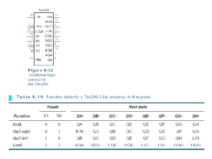
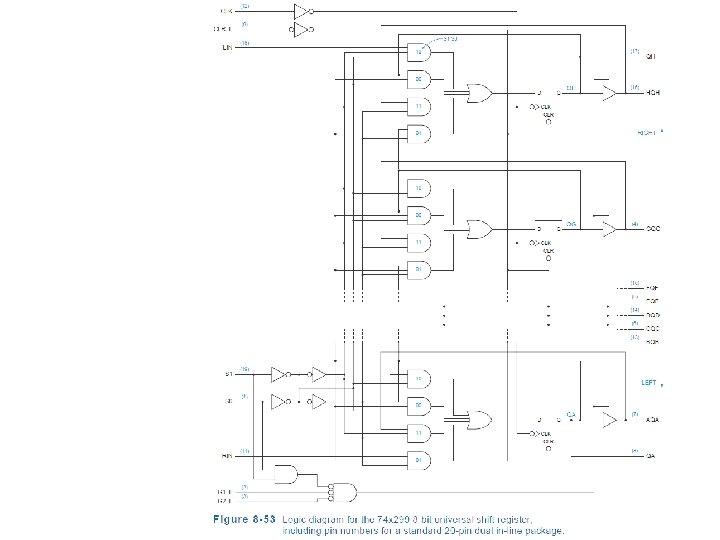
MSI Shift Registers

case s is when “ 00” => qn 1<=q ; When “ 01” => qn 1<= RIN & q(3 downto 1); When “ 10” => qn 1<= q(2 downto 0) & LIN; When “ 11” => qn 1<= d; end case;
- Slides: 47