Design Development and Validation Testing of a Versatile
- Slides: 30

Design, Development and Validation Testing of a Versatile PLD Implementable Single-Chip Heterogeneous, Hybrid and Reconfigurable Multiprocessor Architecture (HDCA) By J. Robert (Bob) Heath**, Sridhar Hegde, Kanchan Bhide, Paul Maxwell, Xiaohui Zhao and Venugopal Duvvuri Department of Electrical and Computer Engineering University of Kentucky Lexington, Kentucky 40506 **heath@engr. uky. edu Heath MAPLD 2005/247 -W

Abstract There appear to be an increasing number of real-time and non-real-time computer applications where the application may be described by process and/or data-flow graphs (from here on we use the term “process flow graphs”). Such applications include radar signal processing, sonar signal processing, various system simulation environments utilized within Computer Aided Design (CAD) software systems, communications signal processing, routing, collection and processing of data from multiple sensors/instruments, its storage, etc. For such applications, a first goal is the availability of a computer system/architecture platform which will allow an application described by a process flow graph of any topology to be mapped to and executed on the computer system/architecture. The application process flow graph could be single or multiple input/output and cyclic or acyclic. Processes are represented by nodes of the graphs. Further, it would be desirable for the computer system/architecture to be able to continue execution of the application with minimum interruption if the application process flow graph topology were to dynamically change during application execution. This goal is referred to as application level reconfigurability. A second goal for the same computer system/architecture would be that it have the ability to dynamically on-the-fly configure, move, or assign processors or other physical resources to application processes (and/or vice versa, the assignment of additional copies of a process to additional processors) that may need them at any time. This goal is referred to as node level reconfigurability. A third goal for the same computer system/architecture would be that it be a single-chip heterogeneous multiprocessor system and that it would have the capability to dynamically on-the-fly configure and reconfigure, if and when needed, single processor architectures within the overall multiprocessor architecture. We refer to this goal as processor architecture level reconfigurability. With proper Operating System (OS) and other system software support, a computer system/architecture platform which can meet these three goals should be able to execute a wide range of non-real and real-time applications described by process flow graphs of any topology in a fault tolerant manner. The contributions of this paper are in that it describes the research and development and current status of the development, testing and evaluation of such a computer system architecture. HDL “virtual prototype” functional and performance simulation testing results are shown for the architecture executing simple hypothetical applications. Future research, development and testing of the architecture is addressed. The described architecture paradigm and platform is known as a single-chip Hybrid Data/Command Driven Architecture (HDCA) system. A reconfigurable/dynamic production HDCA system would be implemented to Programmable Logic Devices (PLDs). Heath 2 MAPLD 2005/247 -W

Goals, Objectives and Functionality of HDCA System • • • Applicable to a wide-range of applications, especially those modeled by process flow graphs. Heterogeneous Shared-Memory Model Multiprocessor Architecture. Allows a mix of Simple and Complex Special-Purpose and General-Purpose Processors Including Core Processors. Single-Chip Architecture Implemented to Programmable Logic Device (PLD) Technology. May be used for real-time or non-real-time applications. Scalable architecture. Fault-tolerant architecture. May operate in a data-driven or command-driven mode at process level. Supports multithreading, MIMD, SIMD and multiple-copy application modes of operation. For data-driven mode, idea is for a small number of short control-tokens to flow through the architecture rather than more voluminous data. Dynamic/Reconfigurable at the “application level”. Dynamic/Reconfigurable at the “node level”. Dynamic/Reconfigurable at the “processor architecture level”. Heath 3 MAPLD 2005/247 -W

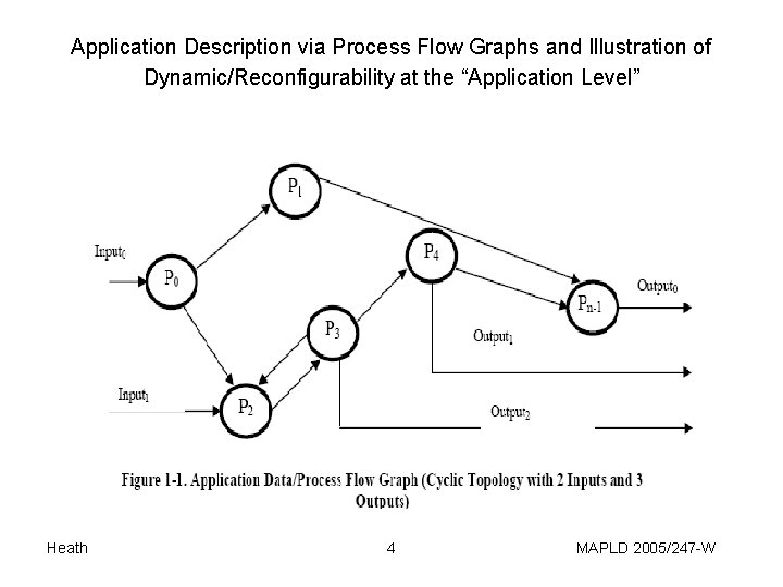
Application Description via Process Flow Graphs and Illustration of Dynamic/Reconfigurability at the “Application Level” Heath 4 MAPLD 2005/247 -W

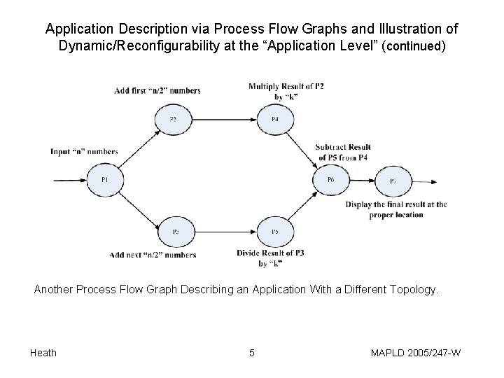
Application Description via Process Flow Graphs and Illustration of Dynamic/Reconfigurability at the “Application Level” (continued) Another Process Flow Graph Describing an Application With a Different Topology. Heath 5 MAPLD 2005/247 -W

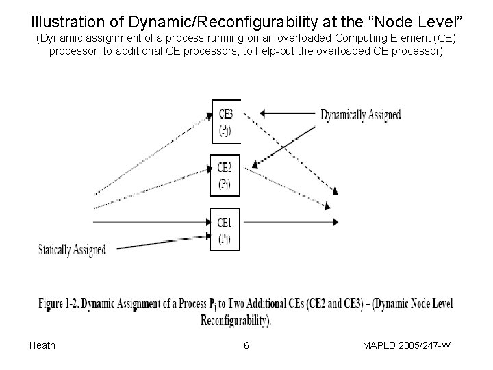
Illustration of Dynamic/Reconfigurability at the “Node Level” (Dynamic assignment of a process running on an overloaded Computing Element (CE) processor, to additional CE processors, to help-out the overloaded CE processor) Heath 6 MAPLD 2005/247 -W

Dynamic/Reconfigurability at the “Processor Architecture Level” Goal - Dynamically, while an application is running, be able to reconfigure (restructure) a Processor Architecture to enhance performance as dynamic changes may occur in application data and process algorithmic structure. Heath 7 MAPLD 2005/247 -W

HDCA System Organization and Architecture (High-Level Functional View) Heath 8 MAPLD 2005/247 -W

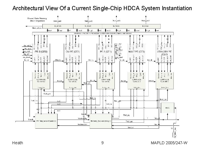
Architectural View Of a Current Single-Chip HDCA System Instantiation Heath 9 MAPLD 2005/247 -W

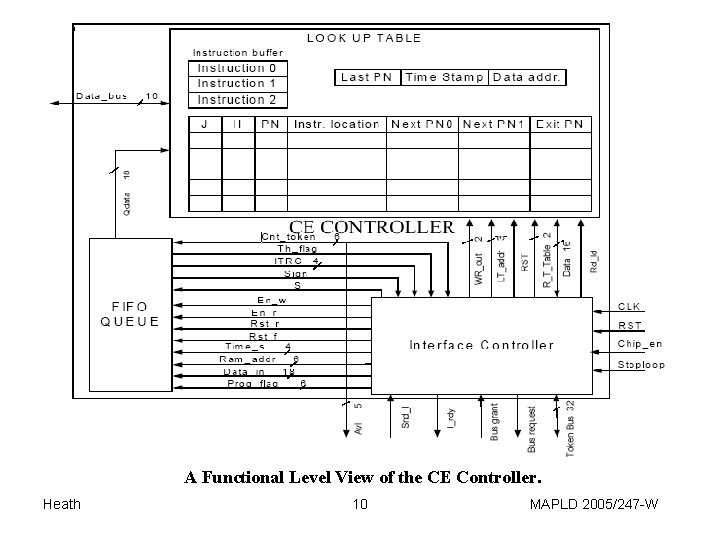
A Functional Level View of the CE Controller. Heath 10 MAPLD 2005/247 -W

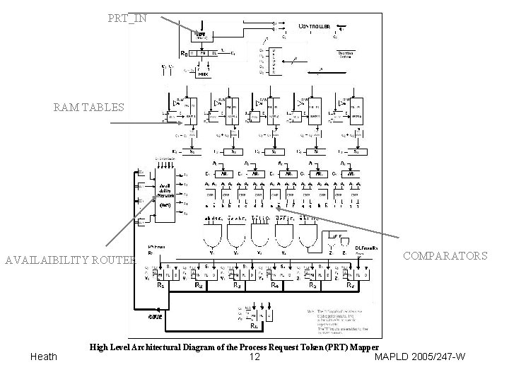
Brief Overview of HDCA Functional Units • Process Request Token (PRT) Mapper. – A Hardware Dynamic Load-Balancing System. – For a Process Requested by a Control Token, It Determines the CE Containing a Copy of the Process Where Wait-Time to Execute the Requested Process is Minimum. CE Input Queue Depth is Used as the Parameter to Determine Minimum Wait Time (Least Depth) to Execution. CE Queue Depth is Directly Proportional to Wait Time via Utilization of “Dummy Tokens”. – Detects Some Faults and System Failures. Heath 11 MAPLD 2005/247 -W

PRT_IN RAM TABLES COMPARATORS AVAILAIBILITY ROUTER Heath High Level Architectural Diagram of the Process Request Token (PRT) Mapper 12 MAPLD 2005/247 -W

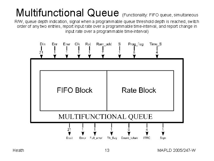
Multifunctional Queue (Functionality: FIFO queue, simultaneous R/W, queue depth indication, signal when a programmable queue threshold depth is reached, switch order of any two entries, report input rate over a programmable time-interval, and report change in input rate over a programmable time-interval) Heath 13 MAPLD 2005/247 -W

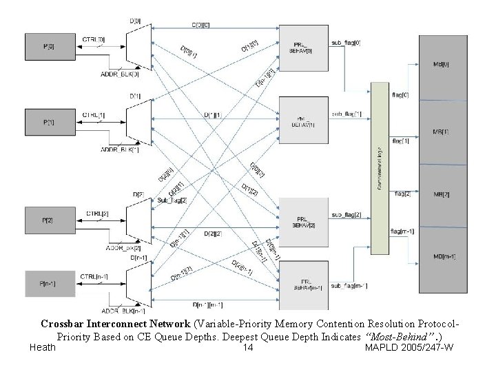
Crossbar Interconnect Network (Variable-Priority Memory Contention Resolution Protocol. Priority Based on CE Queue Depths. Deepest Queue Depth Indicates “Most-Behind”. ) Heath 14 MAPLD 2005/247 -W

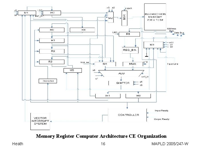
HDCA System CEs (Processors) for Previously Shown Instantiation • Memory Register Computer Architecture CE – For ALU Instructions, one operand in Memory and another in Register. – 16 -Bit Wide Words/Operands. – 16 and 32 -Bit Wide Instructions. – Sixteen Assembly Language Instructions. – I/O Structure. – Hardware Vectored Priority Interrupt System, etc. Heath 15 MAPLD 2005/247 -W

Memory Register Computer Architecture CE Organization Heath 16 MAPLD 2005/247 -W

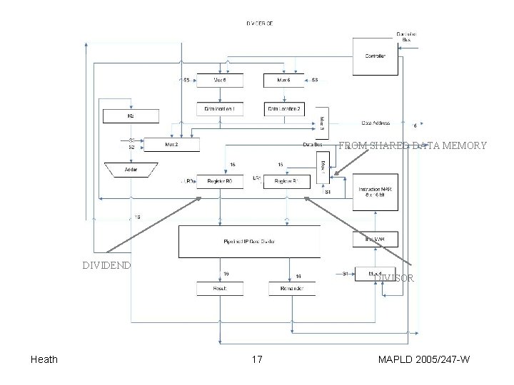
FROM SHARED DATA MEMORY DIVIDEND DIVISOR Heath 17 MAPLD 2005/247 -W

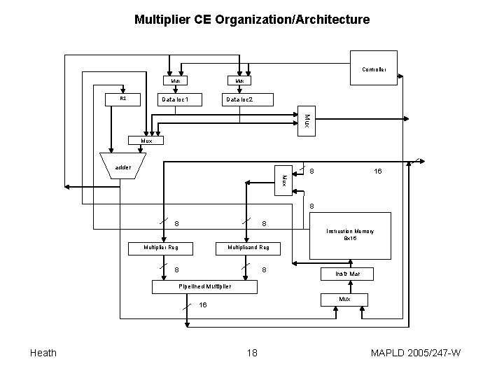
Multiplier CE Organization/Architecture Controller R 2 Mux Data loc 1 Data loc 2 Mux adder Mux 8 16 8 8 8 Instruction Memory 8 x 16 Multiplier Reg Multiplicand Reg 8 8 Instr Mar Pipelined Multiplier Mux 16 Heath 18 MAPLD 2005/247 -W

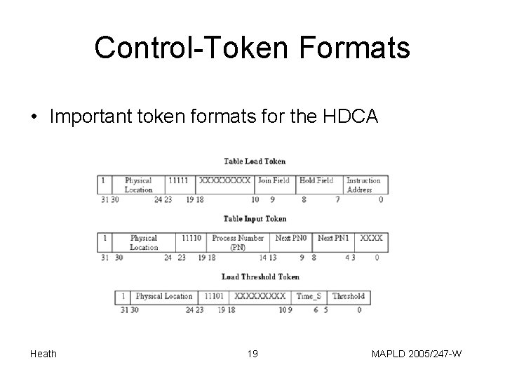
Control-Token Formats • Important token formats for the HDCA Heath 19 MAPLD 2005/247 -W

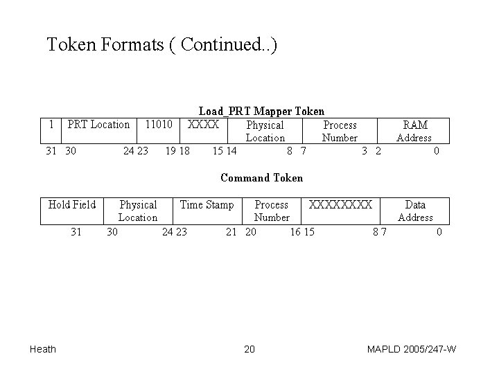
Token Formats ( Continued. . ) Heath 20 MAPLD 2005/247 -W

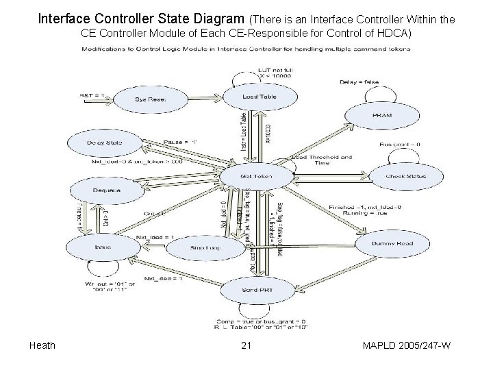
Interface Controller State Diagram (There is an Interface Controller Within the CE Controller Module of Each CE-Responsible for Control of HDCA) Heath 21 MAPLD 2005/247 -W

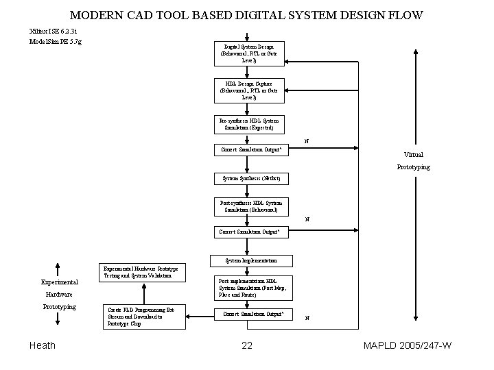
MODERN CAD TOOL BASED DIGITAL SYSTEM DESIGN FLOW Xilinx ISE 6. 2. 3 i Model. Sim PE 5. 7 g Digital System Design (Behavioral, RTL or Gate Level) HDL Design Capture (Behavioral, , RTL or Gate Level) Pre-synthesis HDL System Simulation (Expected) N Correct Simulation Output? Virtual Prototyping System Synthesis (Netlist) Post-synthesis HDL System Simulation (Behavioral) N Correct Simulation Output? System Implementation Experimental Hardware Prototype Testing and System Validation Hardware Prototyping Heath Create PLD Programming Bit. Stream and Download to Prototype Chip Post-implementation HDL System Simulation (Post Map, Place and Route) Correct Simulation Output? 22 N MAPLD 2005/247 -W

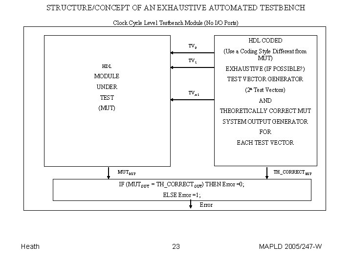
STRUCTURE/CONCEPT OF AN EXHAUSTIVE AUTOMATED TESTBENCH Clock Cycle Level Testbench Module (No I/O Ports) HDL CODED TV 0 (Use a Coding Style Different from MUT) TV 1 HDL EXHAUSTIVE (IF POSSIBLE? ) MODULE TEST VECTOR GENERATOR UNDER (2 n Test Vectors) TVn-1 TEST AND (MUT) THEORETICALLY CORRECT MUT SYSTEM OUTPUT GENERATOR FOR EACH TEST VECTOR MUTOUT TH_CORRECTOUT IF (MUTOUT = TH_CORRECTOUT) THEN Error =0; ELSE Error =1; Error Heath 23 MAPLD 2005/247 -W

Hardware Description Language (HDL) Description of HDCA System • VHDL Used as HDL. • Mostly Behavioral and RTL Level Coding Style Used. • Top-Down HDCA System Architecture Development and Design Style Used. • Structural Bottom-Up Coding and Testing Style Used (Lower Level Functional Units First Described and Tested Before Being Integrated Into Higher Level Functional Units). • Generic and Parameterized Coding Style Used When Applicable. • Approximately 150 Pages (8. 5” x 11”) of Single-Spaced 10 -Point Font VHDL Code for Shown 5 CE Configuration. Heath 24 MAPLD 2005/247 -W

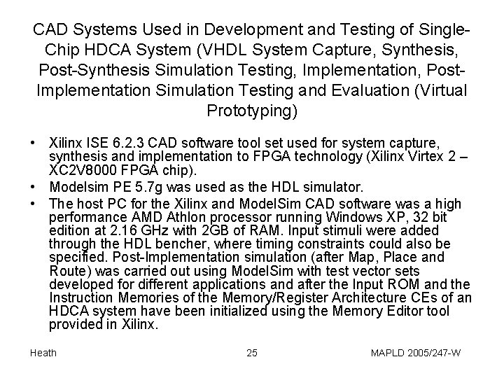
CAD Systems Used in Development and Testing of Single. Chip HDCA System (VHDL System Capture, Synthesis, Post-Synthesis Simulation Testing, Implementation, Post. Implementation Simulation Testing and Evaluation (Virtual Prototyping) • Xilinx ISE 6. 2. 3 CAD software tool set used for system capture, synthesis and implementation to FPGA technology (Xilinx Virtex 2 – XC 2 V 8000 FPGA chip). • Modelsim PE 5. 7 g was used as the HDL simulator. • The host PC for the Xilinx and Model. Sim CAD software was a high performance AMD Athlon processor running Windows XP, 32 bit edition at 2. 16 GHz with 2 GB of RAM. Input stimuli were added through the HDL bencher, where timing constraints could also be specified. Post-Implementation simulation (after Map, Place and Route) was carried out using Model. Sim with test vector sets developed for different applications and after the Input ROM and the Instruction Memories of the Memory/Register Architecture CEs of an HDCA system have been initialized using the Memory Editor tool provided in Xilinx. Heath 25 MAPLD 2005/247 -W

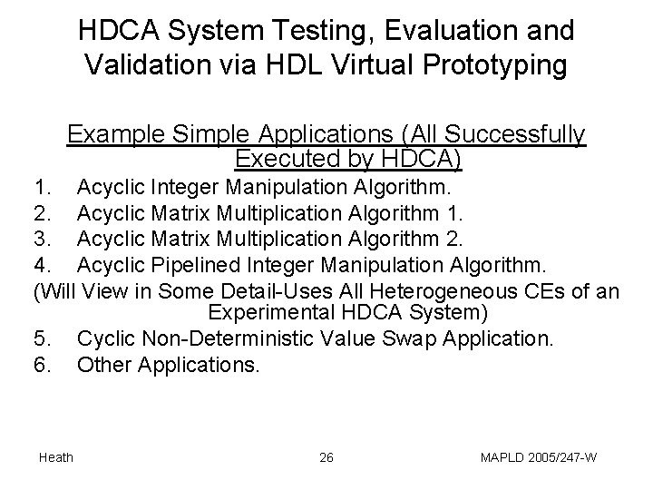
HDCA System Testing, Evaluation and Validation via HDL Virtual Prototyping Example Simple Applications (All Successfully Executed by HDCA) 1. Acyclic Integer Manipulation Algorithm. 2. Acyclic Matrix Multiplication Algorithm 1. 3. Acyclic Matrix Multiplication Algorithm 2. 4. Acyclic Pipelined Integer Manipulation Algorithm. (Will View in Some Detail-Uses All Heterogeneous CEs of an Experimental HDCA System) 5. Cyclic Non-Deterministic Value Swap Application. 6. Other Applications. Heath 26 MAPLD 2005/247 -W

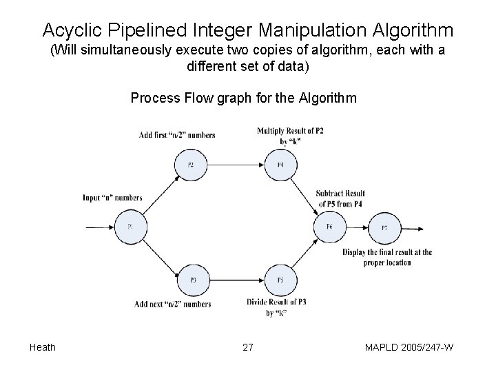
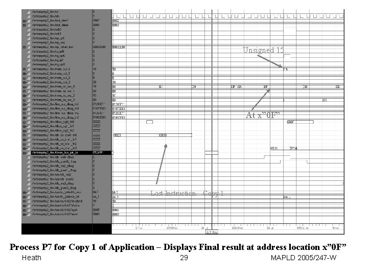
Acyclic Pipelined Integer Manipulation Algorithm (Will simultaneously execute two copies of algorithm, each with a different set of data) Process Flow graph for the Algorithm Heath 27 MAPLD 2005/247 -W

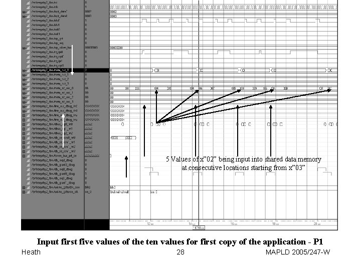
5 Values of x” 02” being input into shared data memory at consecutive locations starting from x” 03” Input first five values of the ten values for first copy of the application - P 1 Heath 28 MAPLD 2005/247 -W

Unsigned 15 At x” 0 F” Last Instruction – Copy 1 Process P 7 for Copy 1 of Application – Displays Final result at address location x” 0 F” Heath 29 MAPLD 2005/247 -W

Conclusions and Future Research • • Conclusions – Validation of the Concept of a HDCA Accomplished via Virtual Prototyping – Parallel Single-Chip Multiprocessor System, Hybrid, Heterogeneous, Dynamic/Reconfigurable at Application and Node Levels, Implementable to PLD Technology, etc. – Scalable Architecture/Design at the same time also a So. C. – Can Simultaneously Execute Multiple Copies of an Application, each with different sets of data. – Potential for Execution of a Wide Range of Applications (Radar signal processing; communications (packet driven) processing; image (pixel driven) processing; satellite data-stream processing; embedded computing applications including control applications; collection, processing and storage of data from multiple sensors/instruments, etc) – Can Execute More Complex Applications. Future Research – Include More Complex Processors Into Experimental Model of HDCA In Addition to an Operating System (Linux, etc? ). – Further Research Into Development and Refinement of the Concept of “Reconfigurability at the Processor Architecture Level”. – Identification and Adaptation to Several “Real Applications”!! Heath 30 MAPLD 2005/247 -W