Design Consideration of Using Zynq HLS to Implement




- Slides: 19

Design Consideration of Using Zynq & HLS to Implement Face Detection Algorithm © Copyright 2013 Xilinx.

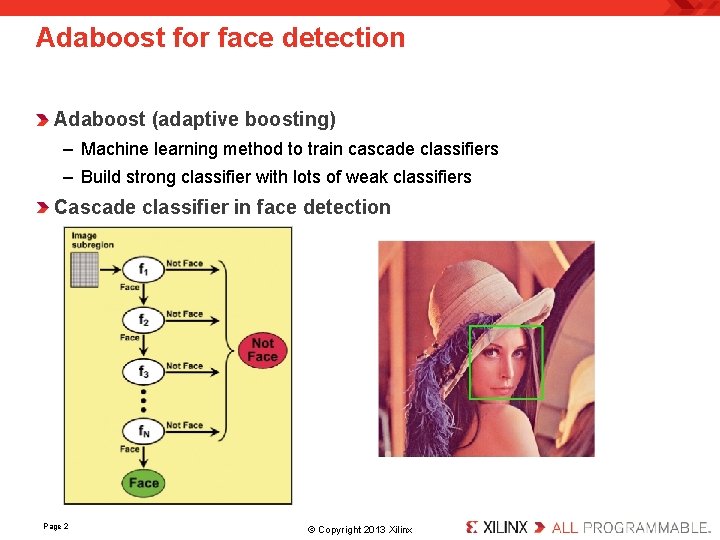
Adaboost for face detection Adaboost (adaptive boosting) – Machine learning method to train cascade classifiers – Build strong classifier with lots of weak classifiers Cascade classifier in face detection Page 2 . © Copyright 2013 Xilinx.

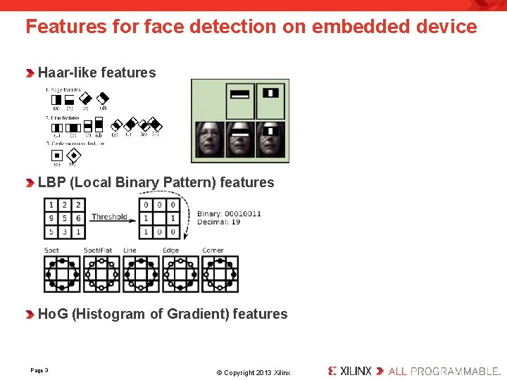
Features for face detection on embedded device Haar-like features LBP (Local Binary Pattern) features Ho. G (Histogram of Gradient) features Page 3 . © Copyright 2013 Xilinx.

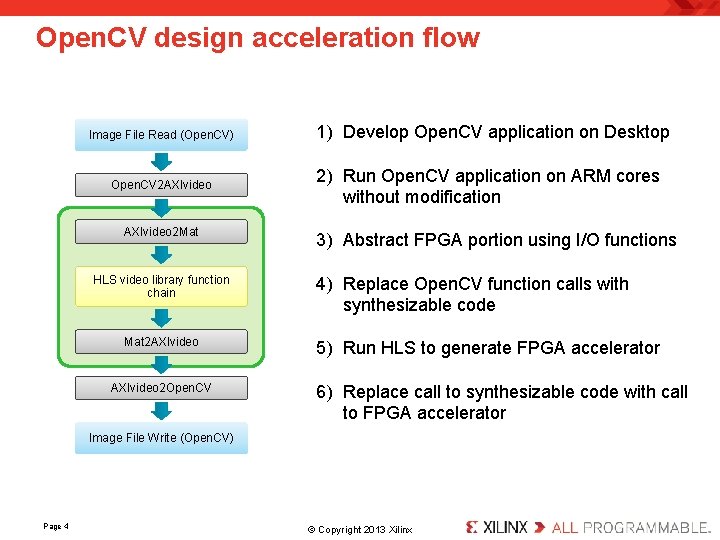
Open. CV design acceleration flow Image File Read (Open. CV) Open. CV 2 AXIvideo 2 Mat HLS video library function chain Mat 2 AXIvideo 2 Open. CV 1) Develop Open. CV application on Desktop 2) Run Open. CV application on ARM cores without modification 3) Abstract FPGA portion using I/O functions 4) Replace Open. CV function calls with synthesizable code 5) Run HLS to generate FPGA accelerator 6) Replace call to synthesizable code with call to FPGA accelerator Image File Write (Open. CV) Page 4 . © Copyright 2013 Xilinx.

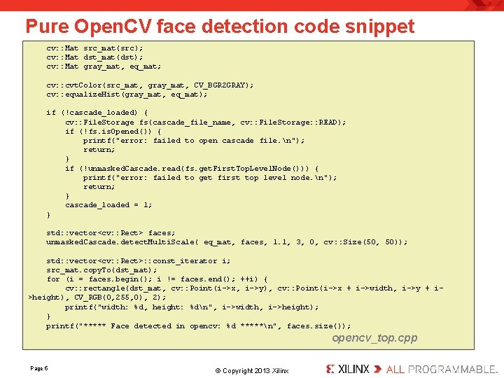
Pure Open. CV face detection code snippet cv: : Mat src_mat(src); cv: : Mat dst_mat(dst); cv: : Mat gray_mat, eq_mat; cv: : cvt. Color(src_mat, gray_mat, CV_BGR 2 GRAY); cv: : equalize. Hist(gray_mat, eq_mat); if (!cascade_loaded) { cv: : File. Storage fs(cascade_file_name, cv: : File. Storage: : READ); if (!fs. is. Opened()) { printf("error: failed to open cascade file. n"); return; } if (!unmasked. Cascade. read(fs. get. First. Top. Level. Node())) { printf("error: failed to get first top level node. n"); return; } cascade_loaded = 1; } std: : vector<cv: : Rect> faces; unmasked. Cascade. detect. Multi. Scale( eq_mat, faces, 1. 1, 3, 0, cv : : Size(50, 50)); std: : vector<cv: : Rect>: : const_iterator i; src_mat. copy. To(dst_mat); for (i = faces. begin(); i != faces. end(); ++i) { cv: : rectangle(dst_mat, cv: : Point(i->x, i->y), cv: : Point(i->x + i->width, i->y + i>height), CV_RGB(0, 255, 0), 2); printf("width: %d, height: %dn", i->width, i->height); } printf("***** Face detected in opencv: %d *****n", faces. size()); opencv_top. cpp Page 5 . © Copyright 2013 Xilinx.

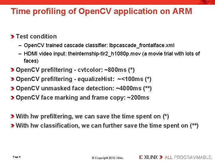
Time profiling of Open. CV application on ARM Test condition – Open. CV trained cascade classifier: lbpcascade_frontalface. xml – HDMI video input: theinternship-tlr 2_h 1080 p. mov (a movie trial with lots of faces) Open. CV prefiltering - cvtcolor: ~800 ms (*) Open. CV prefiltering - equalize. Hist: ~<100 ms (*) Open. CV unmasked face detection: ~4000 ms (**) Open. CV face marking and frame copy: ~200 ms With hw prefiltering, we can save the time spent on (*) With hw classification, we can further save the time spent on (**) Page 6 . © Copyright 2013 Xilinx.

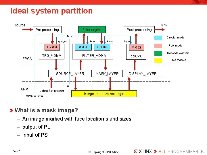
Ideal system partition source sink Pre-processing Filter engine Post-processing Mux Circular mode fsync_out S 2 MM FPGA MM 2 S TPG_VDMA fsync S 2 MM MM 2 S FILTER_VDMA logi. CVC MASK_LAYER DISPLAY_LAYER sel video file reader GPIO: ext_fsync Merge and draw rectangle What is a mask image? – An image marked with face location s and sizes – output of PL – input of PS Page 7 Cascade classifier Face marker SOURCE_LAYER ARM Park mode . © Copyright 2013 Xilinx.

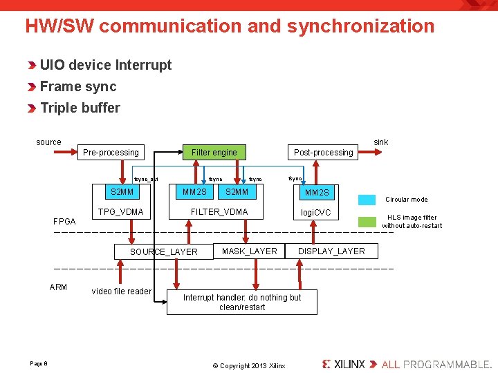
HW/SW communication and synchronization UIO device Interrupt Frame sync Triple buffer source sink Pre-processing Filter engine fsync_out S 2 MM TPG_VDMA fsync MM 2 S Post-processing S 2 MM MM 2 S FILTER_VDMA logi. CVC FPGA SOURCE_LAYER ARM Page 8 video file reader fsync MASK_LAYER DISPLAY_LAYER Interrupt handler: do nothing but clean/restart . © Copyright 2013 Xilinx. Circular mode HLS image filter without auto-restart

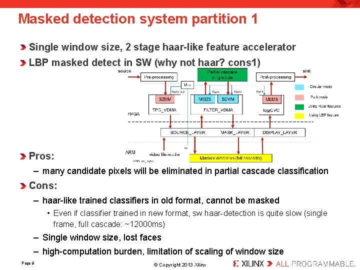
Masked detection system partition 1 Single window size, 2 stage haar-like feature accelerator LBP masked detect in SW (why not haar? cons 1) Pros: – many candidate pixels will be eliminated in partial cascade classification Cons: – haar-like trained classifiers in old format, cannot be masked • Even if classifier trained in new format, sw haar-detection is quite slow (single frame, full cascade: ~12000 ms) – Single window size, lost faces – high-computation burden, limitation of scaling of window size Page 9 . © Copyright 2013 Xilinx.

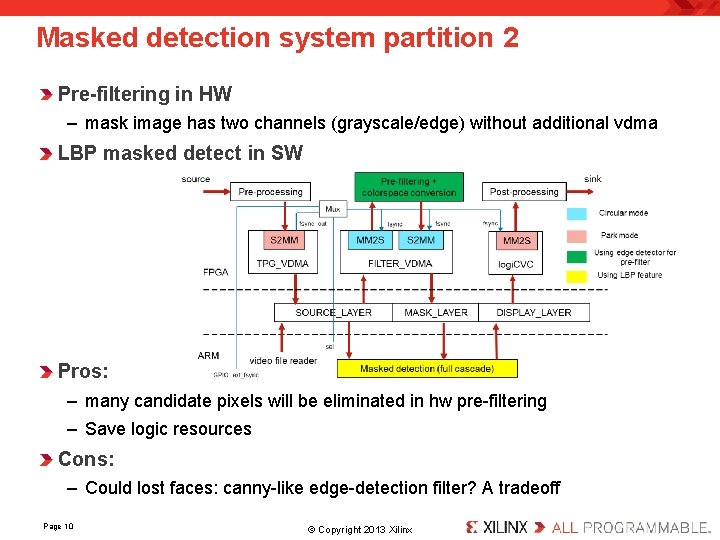
Masked detection system partition 2 Pre-filtering in HW – mask image has two channels (grayscale/edge) without additional vdma LBP masked detect in SW Pros: – many candidate pixels will be eliminated in hw pre-filtering – Save logic resources Cons: – Could lost faces: canny-like edge-detection filter? A tradeoff Page 10 . © Copyright 2013 Xilinx.

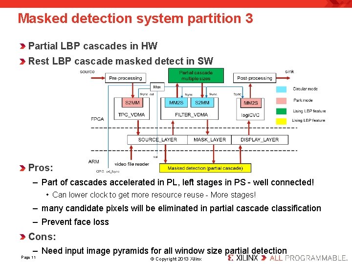
Masked detection system partition 3 Partial LBP cascades in HW Rest LBP cascade masked detect in SW Pros: – Part of cascades accelerated in PL, left stages in PS - well connected! • Can lower clock to get more resource reuse - More stages! – many candidate pixels will be eliminated in partial cascade classification – Prevent face loss Cons: – Need input image pyramids for all window size partial detection Page 11 . © Copyright 2013 Xilinx.

An example of face detection algorithm implementation Xilinx Confidential . © Copyright 2013 Xilinx.

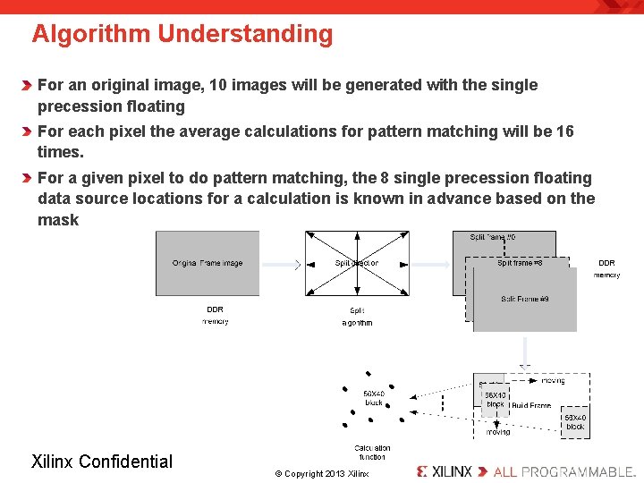
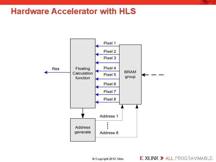
Algorithm Understanding For an original image, 10 images will be generated with the single precession floating For each pixel the average calculations for pattern matching will be 16 times. For a given pixel to do pattern matching, the 8 single precession floating data source locations for a calculation is known in advance based on the mask Xilinx Confidential . © Copyright 2013 Xilinx.

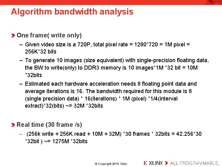
Algorithm bandwidth analysis One frame( write only) – Given video size is a 720 P, total pixel rate = 1280*720 = 1 M pixel = 256 K*32 bits – To generate 10 images (size equivalent) with single-precision floating data, the BW to write(only) to DDR 3 memory is 10 images*1 M *32 bit = 10 M *32 bits – Estimated each hardware acceleration needs 8 floating point data and average iterations is 16. The bandwidth required for this module is 8 (single precision data) * 16(iterations) * 1 M (pixel) *1/4(interval extract)*32(bits) ~= 32 M *32 bits Real time (30 frame /s) – (256 k write + 256 K read + 10 M + 32 M) *30 frames * 32 bits = 42. 256*30 *32 bit ) ~= 1275 M *32 bits . © Copyright 2013 Xilinx.

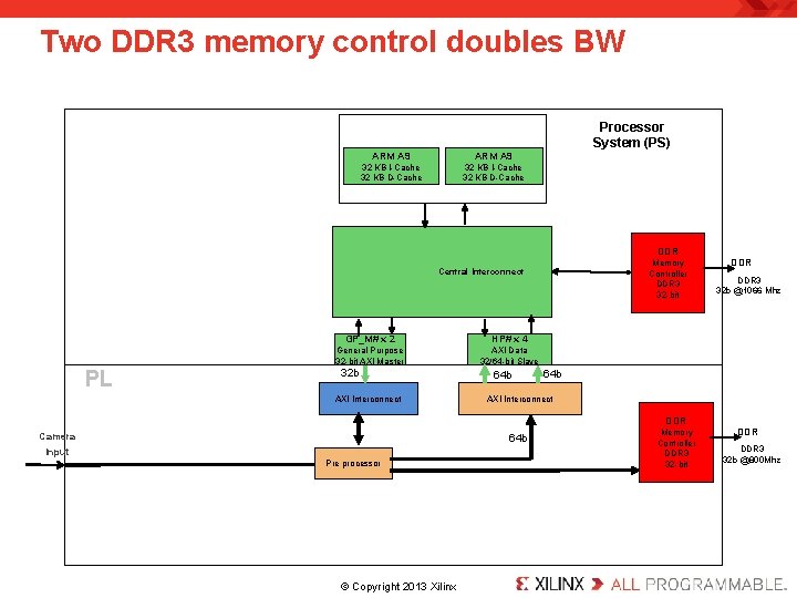
Algorithm bandwidth analysis ~ cont Conclusion: – The algorithm definitely needs 5100 MB/s for real-time performance based on the data flow. – Single 32 bit DDR 3 memory can’t meet this requirement • 1066(Mbps)*0. 6(DDR 3 efficiency) *32 bits(pin) = 2558 MB/s Proposal: – Use one PS DDR 3 control and one PL DDR 3 control to double the bandwidth . © Copyright 2013 Xilinx.

Two DDR 3 memory control doubles BW ARM A 9 32 KB I-Cache 32 KB D-Cache Processor System (PS) DDR Memory Controller DDR 3 32 -bit Central Interconnect PL GP_M# x 2 HP# x 4 General Purpose 32 -bit AXI Master AXI Data 32/64 -bit Slave 32 b 64 b AXI Interconnect 64 b Input Pre processor . © Copyright 2013 Xilinx. DDR 3 32 b @1066 Mhz 64 b DDR Camera DDR Memory Controller DDR 3 32 -bit DDR 3 32 b @800 Mhz

Hardware Accelerator with HLS . © Copyright 2013 Xilinx.

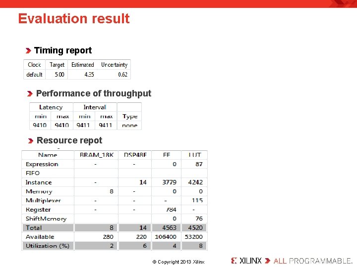
Evaluation result Timing report Performance of throughput Resource repot . © Copyright 2013 Xilinx.

Summary 8 pixels Calculating operation can run at per clock cycle. (Interval = 9000 + 324 + latency of calculation function). Per calculation function run time = (9411/9000)*5 ns = 5. 23 ns. When LUTs utilization is up to 64%, 8*parallel calculation function run time = 5. 23/8 ns = 0. 6535 ns for each calculation. That is to say, up to 1500 MHz/s calculating frequency. . © Copyright 2013 Xilinx.