Design and TCAD simulation of a new generation


![PERFORMANCE COMPARISON FBK [4] Signal Efficiency = Ratio of max. signal after irradiation and PERFORMANCE COMPARISON FBK [4] Signal Efficiency = Ratio of max. signal after irradiation and](https://slidetodoc.com/presentation_image/256c343b7852b5963956566b669223e7/image-22.jpg)
- Slides: 22

Design and TCAD simulation of a new generation of 3 D Sensors for HL-LHC within the INFN (ATLAS-CMS) R&D program in collaboration with FBK Roberto Mendicino, Gian-Franco Dalla Betta, D M S Sultan Maurizio Boscardin, Gabriele Giacomini, Nicola Zorzi, Sabina Ronchin 10 th TREDI Workshop Trento, Italy 17 th February-19 th February 2015

Outline • Introduction: Modified 3 D sensor technology at FBK • New technology developed for new thin sensors generation • Layout design • TCAD Simulation: • Electrical simulation • Functional results for irradiated sensors • Conclusions

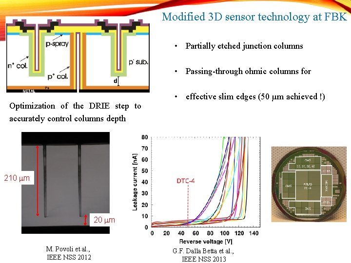
Modified 3 D sensor technology at FBK • Partially etched junction columns • Passing-through ohmic columns for Optimization of the DRIE step to accurately control columns depth • effective slim edges (50 µm achieved !) 210 mm 20 mm M. Povoli et al. , IEEE NSS 2012 G. F. Dalla Betta et al. , IEEE NSS 2013

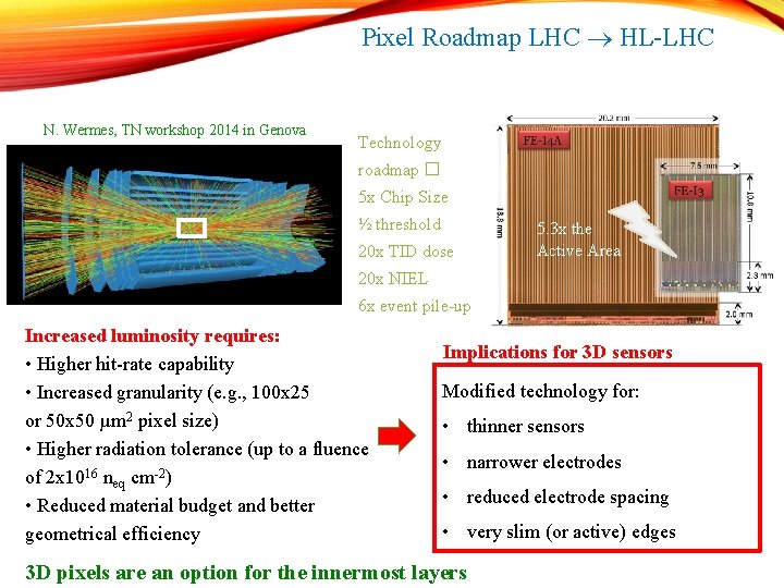
Pixel Roadmap LHC HL-LHC N. Wermes, TN workshop 2014 in Genova Technology roadmap � 5 x Chip Size ½ threshold 20 x TID dose 5. 3 x the Active Area 20 x NIEL 6 x event pile-up Increased luminosity requires: • Higher hit-rate capability • Increased granularity (e. g. , 100 x 25 or 50 x 50 µm 2 pixel size) • Higher radiation tolerance (up to a fluence of 2 x 10¹⁶ neq cm-2) • Reduced material budget and better geometrical efficiency Implications for 3 D sensors Modified technology for: • thinner sensors • narrower electrodes • reduced electrode spacing • very slim (or active) edges 3 D pixels are an option for the innermost layers

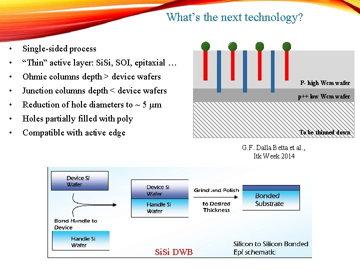
What’s the next technology? • Single-sided process • “Thin” active layer: Si. Si, SOI, epitaxial … • Ohmic columns depth > device wafers • Junction columns depth < device wafers • Reduction of hole diameters to ~ 5 µm • Holes partially filled with poly • Compatible with active edge P- high Wcm wafer p++ low Wcm wafer To be thinned down G. F. Dalla Betta et al. , Itk Week 2014 Si. Si DWB

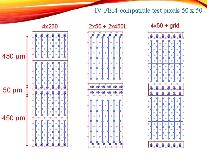
IV FEI 4 -compatible test pixels 50 x 50 4 x 250 450 mm 2 x 50 + 2 x 450 L 4 x 50 + grid

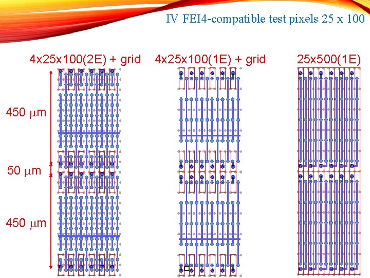
IV FEI 4 -compatible test pixels 25 x 100 4 x 25 x 100(2 E) + grid 450 mm 4 x 25 x 100(1 E) + grid 25 x 500(1 E)

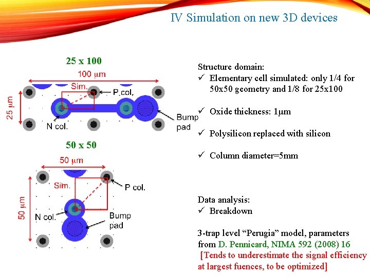
IV Simulation on new 3 D devices 25 x 100 Structure domain: ü Elementary cell simulated: only 1/4 for 50 x 50 geometry and 1/8 for 25 x 100 ü Oxide thickness: 1µm ü Polysilicon replaced with silicon 50 x 50 ü Column diameter=5 mm Data analysis: ü Breakdown 3 -trap level “Perugia” model, parameters from D. Pennicard, NIMA 592 (2008) 16 [Tends to underestimate the signal efficiency at largest fuences, to be optimized]

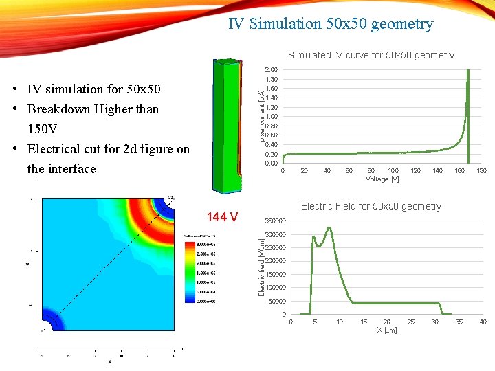
IV Simulation 50 x 50 geometry Simulated IV curve for 50 x 50 geometry 2. 00 1. 80 pixel current [p. A] • IV simulation for 50 x 50 • Breakdown Higher than 150 V • Electrical cut for 2 d figure on the interface 1. 60 1. 40 1. 20 1. 00 0. 80 0. 60 0. 40 0. 20 0. 00 0 20 40 60 80 100 120 140 160 180 35 40 Voltage [V] Electric Field for 50 x 50 geometry 144 V 350000 Electric field [V/cm] 300000 250000 200000 150000 100000 50000 0 0 5 10 15 20 X [µm] 25 30

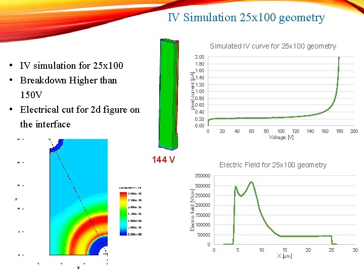
IV Simulation 25 x 100 geometry Simulated IV curve for 25 x 100 geometry 2. 00 • IV simulation for 25 x 100 • Breakdown Higher than 150 V • Electrical cut for 2 d figure on the interface pixel current [p. A] 1. 80 1. 60 1. 40 1. 20 1. 00 0. 80 0. 60 0. 40 0. 20 0. 00 0 20 40 60 80 100 120 140 160 180 200 Voltage [V] 144 V Electric Field for 25 x 100 geometry 350000 Electric field [V/cm] 300000 250000 200000 150000 100000 50000 0 0 5 10 15 X [µm] 20 25 30

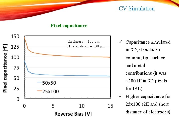
CV Simulation Pixel capacitance Thickness = 150 µm N+ col. depth = 130 µm ü Capacitance simulated in 3 D, it includes column, tip, surface and metal contributions (it was ~200 f. F in 3 D pixels for IBL). ü Higher capacitance for 25 x 100 (2 E and short distance of electrodes)

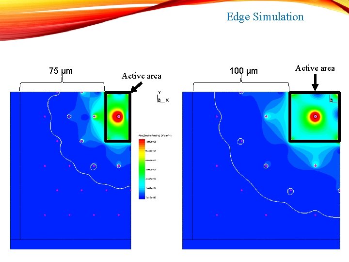
Edge Simulation 75 µm Active area 100 µm Active area

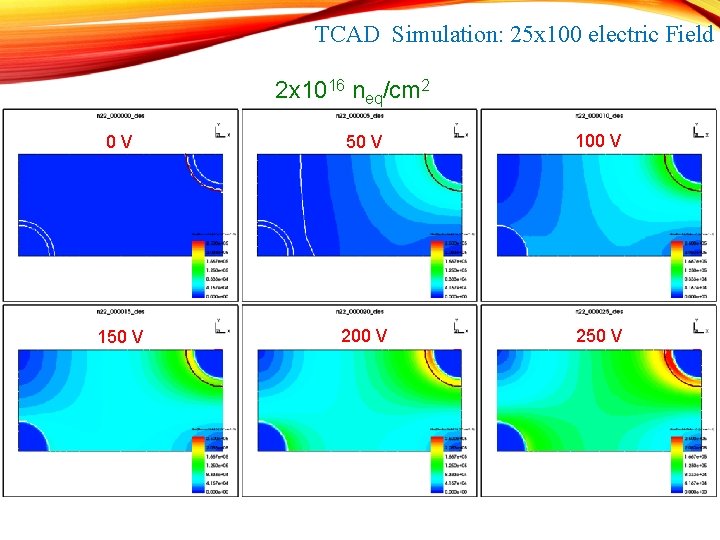
TCAD Simulation: 25 x 100 electric Field 2 x 10¹⁶ neq/cm 2 0 V 50 V 100 V 150 V 200 V 250 V

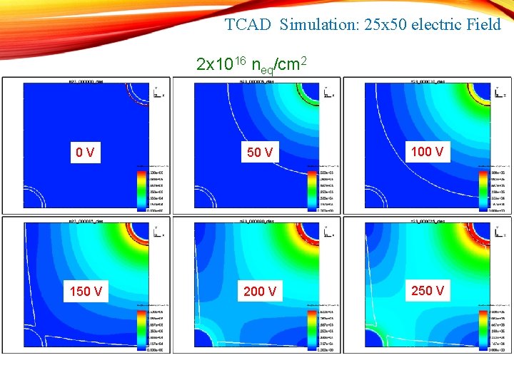
TCAD Simulation: 25 x 50 electric Field 2 x 10¹⁶ neq/cm 2 0 V 50 V 100 V 150 V 200 V 250 V

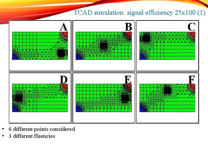
TCAD simulation: signal efficiency 25 x 100 (1) • 6 different points considered • 3 different fluencies

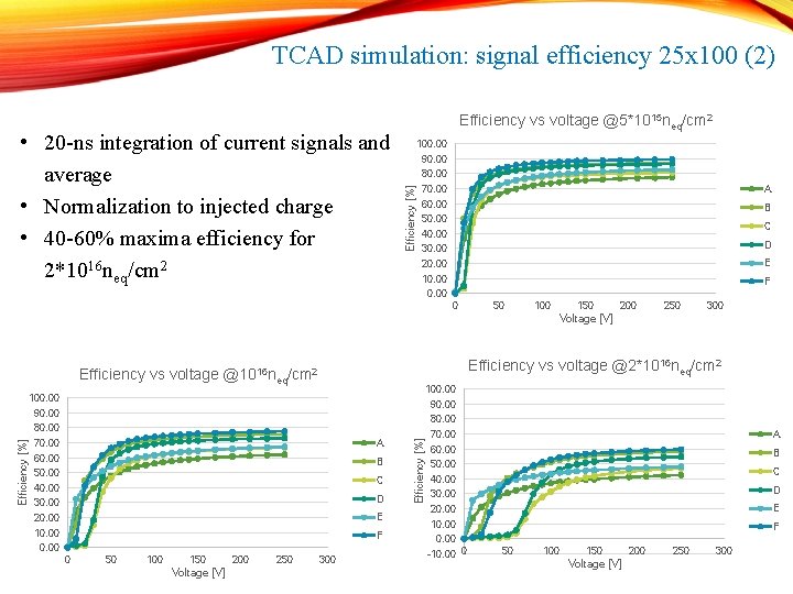
TCAD simulation: signal efficiency 25 x 100 (2) 100. 00 90. 00 80. 00 Efficiency [%] • 20 -ns integration of current signals and average • Normalization to injected charge • 40 -60% maxima efficiency for 2*1016 neq/cm 2 Efficiency vs voltage @5*1015 neq/cm 2 70. 00 A 60. 00 B 50. 00 C 40. 00 30. 00 D 20. 00 E 10. 00 F 0. 00 0 50 100 150 200 250 300 Voltage [V] Efficiency vs voltage @2*1016 neq/cm 2 Efficiency vs voltage @1016 neq/cm 2 100. 00 90. 00 80. 00 70. 00 A 60. 00 B 50. 00 C 40. 00 30. 00 D 20. 00 E 10. 00 F 0. 00 0 50 100 150 Voltage [V] 200 250 300 Efficiency [%] 80. 00 70. 00 A 60. 00 B 50. 00 C 40. 00 30. 00 D 20. 00 E 10. 00 F 0. 00 -10. 00 0 50 100 150 Voltage [V] 200 250 300

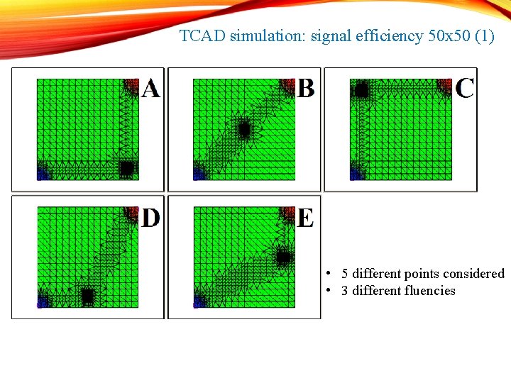
TCAD simulation: signal efficiency 50 x 50 (1) • 5 different points considered • 3 different fluencies

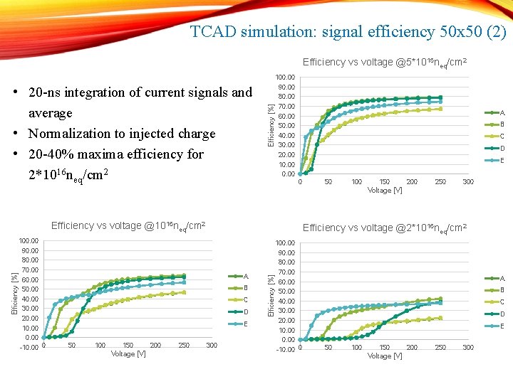
TCAD simulation: signal efficiency 50 x 50 (2) Efficiency vs voltage @5*1015 neq/cm 2 100. 00 90. 00 80. 00 Efficiency [%] • 20 -ns integration of current signals and average • Normalization to injected charge • 20 -40% maxima efficiency for 2*1016 neq/cm 2 70. 00 A 60. 00 50. 00 B 40. 00 C 30. 00 D 20. 00 E 10. 00 0 50 100 150 200 250 300 Voltage [V] Efficiency vs voltage @2*1016 neq/cm 2 100. 00 90. 00 80. 00 70. 00 A 60. 00 50. 00 B 40. 00 C 30. 00 D 20. 00 E 10. 00 -10. 00 0 50 100 150 Voltage [V] 200 250 300 Efficiency [%] Efficiency vs voltage @1016 neq/cm 2 70. 00 A 60. 00 50. 00 B 40. 00 C 30. 00 D 20. 00 E 10. 00 -10. 00 0 50 100 150 Voltage [V] 200 250 300

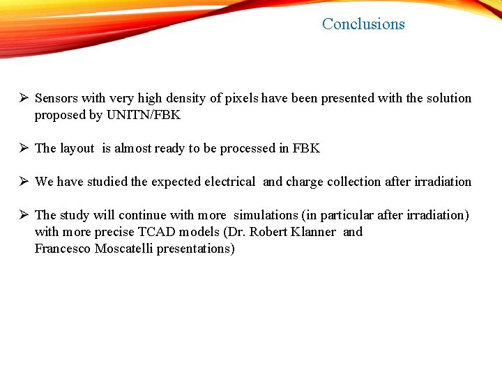
Conclusions Ø Sensors with very high density of pixels have been presented with the solution proposed by UNITN/FBK Ø The layout is almost ready to be processed in FBK Ø We have studied the expected electrical and charge collection after irradiation Ø The study will continue with more simulations (in particular after irradiation) with more precise TCAD models (Dr. Robert Klanner and Francesco Moscatelli presentations)


• backup
![PERFORMANCE COMPARISON FBK 4 Signal Efficiency Ratio of max signal after irradiation and PERFORMANCE COMPARISON FBK [4] Signal Efficiency = Ratio of max. signal after irradiation and](https://slidetodoc.com/presentation_image/256c343b7852b5963956566b669223e7/image-22.jpg)
PERFORMANCE COMPARISON FBK [4] Signal Efficiency = Ratio of max. signal after irradiation and before irradiation C. Da Via, S. Watts, NIMA 603 (2009) 319 [1] ATLAS IBL Collaboration, JINST 7 (2012) P 11010 [2] M. Koehler et al. NIMA 659 (2011) 272 [3] C. Da Via, et al. , NIMA 604 (2009) 505 [4] G. -F. Dalla Betta, et al. , HSTD 9 (2013) Original Compilation by C. Da Via