Design and Post Optimization Flow for Advanced Thermal

![Introduction (2) q Body Bias Control [5] Ø Figure 2 shows leakage current reduction Introduction (2) q Body Bias Control [5] Ø Figure 2 shows leakage current reduction](https://slidetodoc.com/presentation_image_h/90b919e6a42934ccf849919f3af6704a/image-3.jpg)
![References [1] D. Brooks and M. Martonosi, “Dynamic thermal management for high-performance microprocessors, ” References [1] D. Brooks and M. Martonosi, “Dynamic thermal management for high-performance microprocessors, ”](https://slidetodoc.com/presentation_image_h/90b919e6a42934ccf849919f3af6704a/image-13.jpg)
- Slides: 13

Design and Post Optimization Flow for Advanced Thermal Management by Use of Body Bias Hyung-Ock Kim, Jun Seomun, Jaehan Jeon, Chungki Oh, Wook Kim, Kyung-Tae Do, Jung Yun Choi, Hyo-Sig Won, Kee Sup Kim Samsung Electronics, Korea

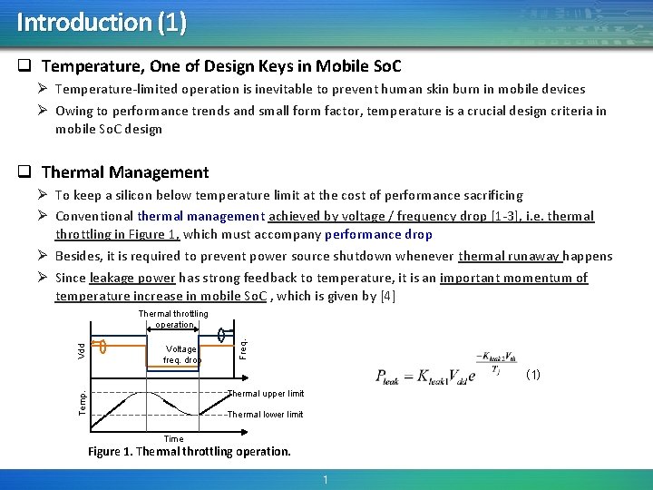
Introduction (1) q Temperature, One of Design Keys in Mobile So. C Ø Temperature-limited operation is inevitable to prevent human skin burn in mobile devices Ø Owing to performance trends and small form factor, temperature is a crucial design criteria in mobile So. C design q Thermal Management Ø To keep a silicon below temperature limit at the cost of performance sacrificing Ø Conventional thermal management achieved by voltage / frequency drop [1 -3], i. e. thermal throttling in Figure 1, which must accompany performance drop Ø Besides, it is required to prevent power source shutdown whenever thermal runaway happens Ø Since leakage power has strong feedback to temperature, it is an important momentum of temperature increase in mobile So. C , which is given by [4] Voltage, freq. drop Freq. Vdd Thermal throttling operation (1) Temp. Thermal upper limit Thermal lower limit Time Figure 1. Thermal throttling operation. 1
![Introduction 2 q Body Bias Control 5 Ø Figure 2 shows leakage current reduction Introduction (2) q Body Bias Control [5] Ø Figure 2 shows leakage current reduction](https://slidetodoc.com/presentation_image_h/90b919e6a42934ccf849919f3af6704a/image-3.jpg)
Introduction (2) q Body Bias Control [5] Ø Figure 2 shows leakage current reduction by use of reverse body bias (RBB) in nanometer-scale technologies Ø RBB can be utilized to relieve thermal throttling by weakening leakage-temperature feedback Figure 2. Leakage current reduction by RBB of 0. 4 V. q Advanced Thermal Design and Management by Body Bias Use Ø We propose body bias design and optimization scheme spanning from system-level design to post silicon tuning to enhance thermal management Ø In design stage, thermal-leakage feedback and body bias design cost are formulated so as to decide body bias use, which is followed by body bias implementation Ø In post silicon, body bias use is explored and optimized both to optimize peak performance and to save total power Ø The proposed scheme has been implemented in 32 nm HKMG commercial mobile So. C, Exynos 4 Quad, and it results in 12. 3% performance improvement in high speed mode and 19. 1% total power saving 2

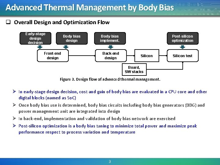
Advanced Thermal Management by Body Bias q Overall Design and Optimization Flow Early-stage design decision Body bias design Front-end design Body bias implement. Back-end design Post-silicon optimization Silicon test Board, SW stacks Figure 3. Design flow of advanced thermal management. Ø In early-stage design decision, cost and gain of body bias are evaluated in a CPU core and other digital blocks (named as So. C) Ø Once body bias use is determined, body bias circuits including body bias generators (BBG) and power management unit are integrated into design Ø In back-end, implementation and validation of body bias network are exercised Ø Post-silicon optimization is a body bias tuning to minimize total power and maximize peak performance respect to process variation and temperature 3

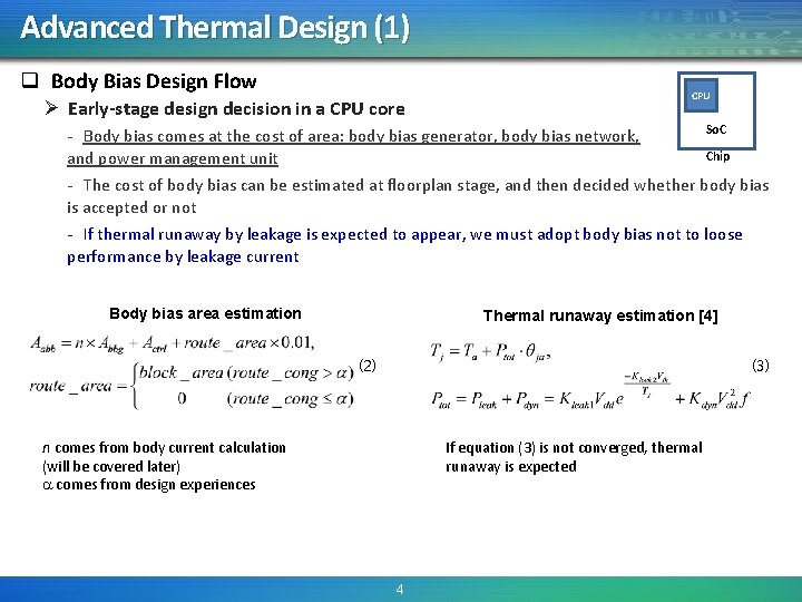
Advanced Thermal Design (1) q Body Bias Design Flow Ø Early-stage design decision in a CPU core CPU So. C - Body bias comes at the cost of area: body bias generator, body bias network, Chip and power management unit - The cost of body bias can be estimated at floorplan stage, and then decided whether body bias is accepted or not - If thermal runaway by leakage is expected to appear, we must adopt body bias not to loose performance by leakage current Body bias area estimation Thermal runaway estimation [4] (2) (3) n comes from body current calculation (will be covered later) comes from design experiences If equation (3) is not converged, thermal runaway is expected 4

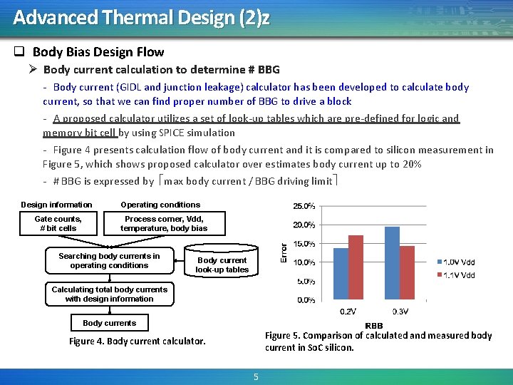
Advanced Thermal Design (2)z q Body Bias Design Flow Ø Body current calculation to determine # BBG - Body current (GIDL and junction leakage) calculator has been developed to calculate body current, so that we can find proper number of BBG to drive a block - A proposed calculator utilizes a set of look-up tables which are pre-defined for logic and memory bit cell by using SPICE simulation - Figure 4 presents calculation flow of body current and it is compared to silicon measurement in Figure 5, which shows proposed calculator over estimates body current up to 20% - # BBG is expressed by max body current / BBG driving limit Design information Gate counts, # bit cells Operating conditions Process corner, Vdd, temperature, body bias Searching body currents in operating conditions Body current look-up tables Calculating total body currents with design information Body currents Figure 5. Comparison of calculated and measured body current in So. C silicon. Figure 4. Body current calculator. 5

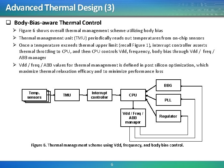
Advanced Thermal Design (3) q Body-Bias-aware Thermal Control Ø Figure 6 shows overall thermal management scheme utilizing body bias Ø Thermal management unit (TMU) periodically reads out temperatures from on-chip sensors Ø Once a temperature exceeds thermal upper limit (recall Figure 1), interrupt controller asserts thermal throttling to CPU, and then CPU controls Vdd, frequency, body bias through Vdd / freq / ABB manager Ø Vdd / freq / ABB values for thermal management is defined in post silicon optimization, which maximize thermal relaxation efficacy and to minimize performance loss BBG Temp. sensors TMU Interrupt controller CPU PLL Vdd / Freq / ABB manager Regulator Figure 6. Thermal management scheme using Vdd, frequency, and body bias control. 6

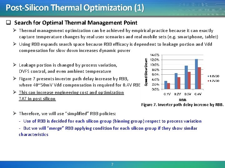
Post-Silicon Thermal Optimization (1) q Search for Optimal Thermal Management Point Ø Thermal management optimization can be achieved by empirical practice because it can exactly capture temperature changes by real user scenarios and real mobile sets (e. g. smartphone, tablet) Ø Using RBB expands search space because RBB efficacy is dependent to leakage portion and Vdd compensation for slow down increases dynamic power Ø Leakage portion is changed by process variation, DVFS control, and even ambient temperature Ø Figure 7 presents inverter path delay increase by RBB, where 40~50 m. V Vdd compensation is required for 0. 4 V RBB Ø This can increase engineering cost and optimization TAT in post silicon Figure 7. Inverter path delay increase by RBB. Ø Therefore, we will use “simplified” RBB policies: - Use of RBB is decided for each silicon group (binning group) respect to process variation - But we will “merge” RBB applying condition for each silicon group if they show similar characteristics 7

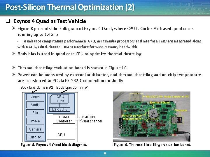
Post-Silicon Thermal Optimization (2) q Exynos 4 Quad as Test Vehicle Ø Figure 8 presents block diagram of Exynos 4 Quad, where CPU is Cortex A 9 -based quad cores running up to 1. 4 GHz - To enhance computation performance, GPU, multimedia processors and interface units are integrated along with 6. 4 GB/s dual-channel DRAM interface for wide memory bandwidth Ø Body bias is used in quad core CPU to optimize thermal throttling Ø Thermal throttling evaluation board is shown in Figure 10 Ø Power can be measured by external multimeter, and thermal throttling and on-chip temperature are transferred to PC via RS-232 -C connection on the fly Body bias domain #2 Body bias domain #1 Video CPU core Audio File Image L 2 Cache DRAM Controller 6. 4 GB/s dual channel Camera Display GPU Figure 9. Thermal throttling evaluation board. Figure 8. Exynos 4 Quad block diagram. 8

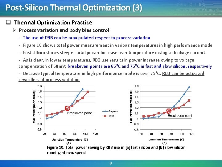
Post-Silicon Thermal Optimization (3) q Thermal Optimization Practice Ø Process variation and body bias control - The use of RBB can be manipulated respect to process variation - Figure 10 shows total power measurement in various temperatures in high performance mode - Fast silicon shows steeper total power increase over temperature owing to leakage current - As is clear, in lower temperatures, RBB use results in power increase owing to voltage compensation of 50 m. V; breakeven points are 65°C and 75°C in fast and slow silicon, respectively - Because typical temperature in high performance mode is over 75°C, RBB can be activated regardless of process variation Breakeven point (b) (a) Figure 10. Total power saving by RBB use in (a) fast silicon and (b) slow silicon running at max speed. 9

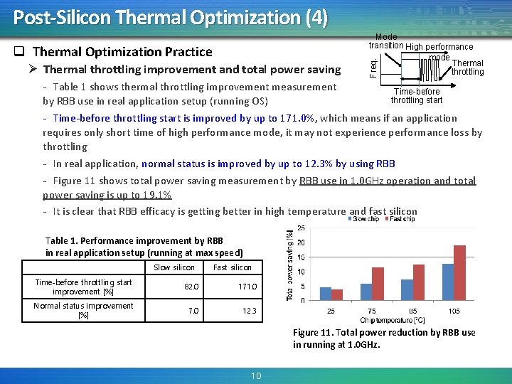
Post-Silicon Thermal Optimization (4) Ø Thermal throttling improvement and total power saving Freq. q Thermal Optimization Practice Mode transition High performance mode Thermal throttling - Table 1 shows thermal throttling improvement measurement Time-before throttling start by RBB use in real application setup (running OS) - Time-before throttling start is improved by up to 171. 0%, which means if an application requires only short time of high performance mode, it may not experience performance loss by throttling - In real application, normal status is improved by up to 12. 3% by using RBB - Figure 11 shows total power saving measurement by RBB use in 1. 0 GHz operation and total power saving is up to 19. 1% - It is clear that RBB efficacy is getting better in high temperature and fast silicon Table 1. Performance improvement by RBB in real application setup (running at max speed) Slow silicon Fast silicon Time-before throttling start improvement [%] 82. 0 171. 0 Normal status improvement [%] 7. 0 12. 3 Figure 11. Total power reduction by RBB use in running at 1. 0 GHz. 10

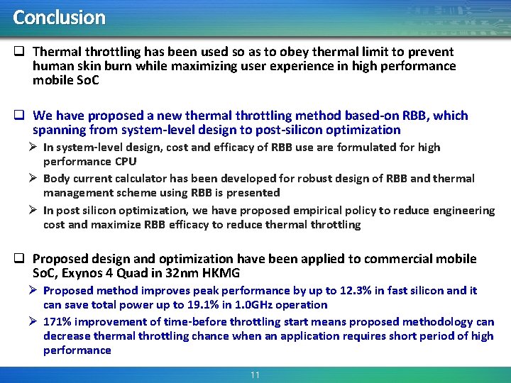
Conclusion q Thermal throttling has been used so as to obey thermal limit to prevent human skin burn while maximizing user experience in high performance mobile So. C q We have proposed a new thermal throttling method based-on RBB, which spanning from system-level design to post-silicon optimization Ø In system-level design, cost and efficacy of RBB use are formulated for high performance CPU Ø Body current calculator has been developed for robust design of RBB and thermal management scheme using RBB is presented Ø In post silicon optimization, we have proposed empirical policy to reduce engineering cost and maximize RBB efficacy to reduce thermal throttling q Proposed design and optimization have been applied to commercial mobile So. C, Exynos 4 Quad in 32 nm HKMG Ø Proposed method improves peak performance by up to 12. 3% in fast silicon and it can save total power up to 19. 1% in 1. 0 GHz operation Ø 171% improvement of time-before throttling start means proposed methodology can decrease thermal throttling chance when an application requires short period of high performance 11
![References 1 D Brooks and M Martonosi Dynamic thermal management for highperformance microprocessors References [1] D. Brooks and M. Martonosi, “Dynamic thermal management for high-performance microprocessors, ”](https://slidetodoc.com/presentation_image_h/90b919e6a42934ccf849919f3af6704a/image-13.jpg)
References [1] D. Brooks and M. Martonosi, “Dynamic thermal management for high-performance microprocessors, ” in Proc. ISCA, pp. 171‒ 182, 2001. [2] K. Skadron and et al, “Temperature-aware micro-architecture: modeling and implementation, ” ACM Transaction on Architecture and Code Optimization, Vol. 1, No. 1, pp. 94‒ 125, 2004. [3] A. Naveh and et al, “Power and thermal management in the Intel Core Duo processor, ” Intel Technology Journal, Vol. 10, No. 2, pp. 109‒ 122, 2006. [4] J. H. Choi, A. Bansal, M. Meterelliyoz, J. Murthy, and K. Roy, “Self-consistent approach to leakage power and temperature estimation to predict thermal runaway in Fin. FET circuits, ” IEEE Transaction on Computer-Aided. Design, Vol. 26, No. 11, pp. 2059‒ 2068, 2007. [5] J. W. Tschanz and et al, “Adaptive body bias for reducing impacts of die-to-die and within-die parameter variations on microprocessor frequency and leakage, ” IEEE Journal of Solid-State Circuits, Vol. 37, No. 11, pp. 1396‒ 1402, 2002. [6] D. Markovic, C. C. Wang, L. P. Alarcon, T. -T. Liu, and J. M. Rabaey, “Ultralow-power design in near-threshold region, ” Proc. IEEE, Vol. 98, Issue 2, pp. 237 -252, 2010. [7] Y. Wang and et al, “A 4. 0 GHz 291 Mb voltage-scalable SRAM design in 32 nm high-κ metal-gate CMOS with integrated power management, ” in Proc. ISSCC, pp. 456‒ 457, 2009. [8] C. -H. Jan and et al, “A 32 nm So. C platform technology with 2 nd generation high-k/metal gate transistors optimized for ultra low power, high performance, and high density product applications, ” in Proc. IEDM, pp. 1‒ 4, 2009. [9] S. Borkar, T. Karnik, S. Narenda, A. Keshavarzi, and V. De, “Parameter variations and impact on circuits and microarchitecture, ” in Proc. Design Automation Conference, June 2003, pp 338‒ 342. 12