Design and Implementation of VLSI Systems EN 0160
![Possible solution: interface to a CMOS inverter 3. 0 Voltage [V] In 2. 0 Possible solution: interface to a CMOS inverter 3. 0 Voltage [V] In 2. 0](https://slidetodoc.com/presentation_image/5c049fafba6852b6de09fe344a810059/image-13.jpg)
- Slides: 15

Design and Implementation of VLSI Systems (EN 0160) Lecture 18: Static Combinational Circuit Design (2/2) Prof. Sherief Reda Division of Engineering, Brown University Spring 2007 [sources: Weste/Addison Wesley – Rabaey/Pearson] S. Reda EN 160 SP’ 07

Last lecture • Conversion of AND/OR circuits to NAND/NOR/INV circuits. • An asymmetric gate favor one input over the other(s). • A skewed gate favor one transition over the other(s). S. Reda EN 160 SP’ 07

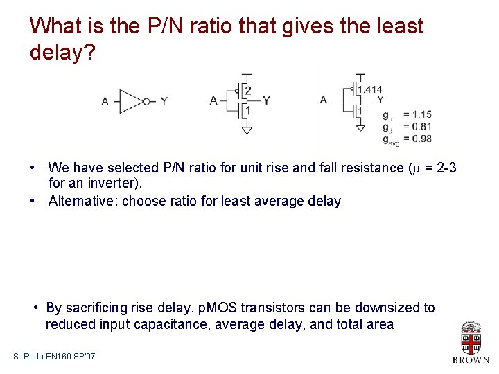
What is the P/N ratio that gives the least delay? • We have selected P/N ratio for unit rise and fall resistance (m = 2 -3 for an inverter). • Alternative: choose ratio for least average delay • By sacrificing rise delay, p. MOS transistors can be downsized to reduced input capacitance, average delay, and total area S. Reda EN 160 SP’ 07

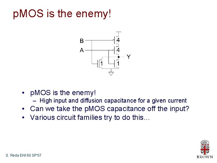
p. MOS is the enemy! • p. MOS is the enemy! – High input and diffusion capacitance for a given current • Can we take the p. MOS capacitance off the input? • Various circuit families try to do this… S. Reda EN 160 SP’ 07

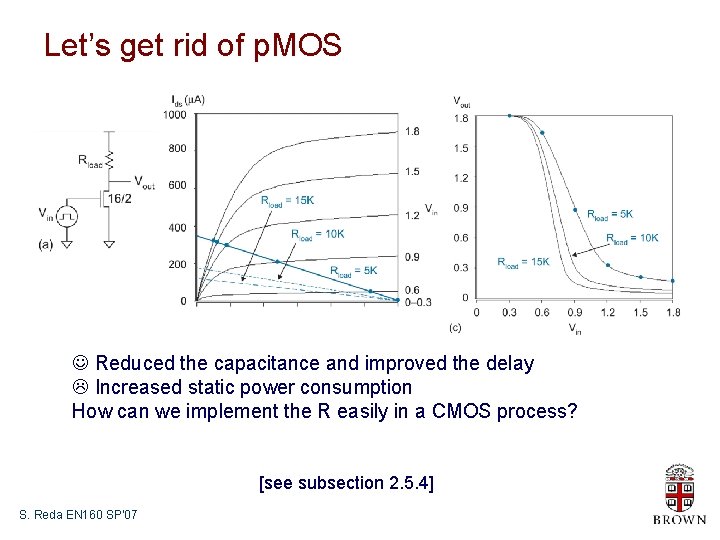
Let’s get rid of p. MOS J Reduced the capacitance and improved the delay L Increased static power consumption How can we implement the R easily in a CMOS process? [see subsection 2. 5. 4] S. Reda EN 160 SP’ 07

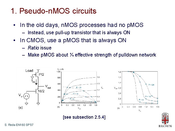
1. Pseudo-n. MOS circuits • In the old days, n. MOS processes had no p. MOS – Instead, use pull-up transistor that is always ON • In CMOS, use a p. MOS that is always ON – Ratio issue – Make p. MOS about ¼ effective strength of pulldown network [see subsection 2. 5. 4] S. Reda EN 160 SP’ 07

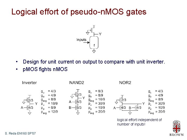
Logical effort of pseudo-n. MOS gates • Design for unit current on output to compare with unit inverter. • p. MOS fights n. MOS logical effort independent of number of inputs! S. Reda EN 160 SP’ 07

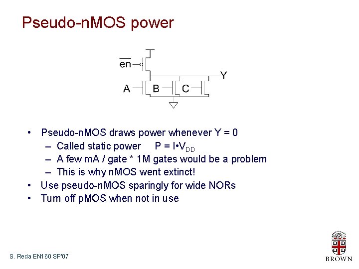
Pseudo-n. MOS power • Pseudo-n. MOS draws power whenever Y = 0 – Called static power P = I • VDD – A few m. A / gate * 1 M gates would be a problem – This is why n. MOS went extinct! • Use pseudo-n. MOS sparingly for wide NORs • Turn off p. MOS when not in use S. Reda EN 160 SP’ 07

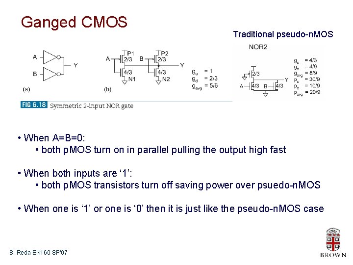
Ganged CMOS Traditional pseudo-n. MOS • When A=B=0: • both p. MOS turn on in parallel pulling the output high fast • When both inputs are ‘ 1’: • both p. MOS transistors turn off saving power over psuedo-n. MOS • When one is ‘ 1’ or one is ‘ 0’ then it is just like the pseudo-n. MOS case S. Reda EN 160 SP’ 07

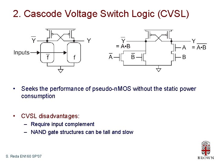
2. Cascode Voltage Switch Logic (CVSL) • Seeks the performance of pseudo-n. MOS without the static power consumption • CVSL disadvantages: – Require input complement – NAND gate structures can be tall and slow S. Reda EN 160 SP’ 07

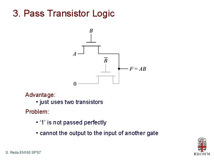
3. Pass Transistor Logic Advantage: • just uses two transistors Problem: • ‘ 1’ is not passed perfectly • cannot the output to the input of another gate S. Reda EN 160 SP’ 07

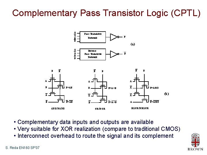
Complementary Pass Transistor Logic (CPTL) A A B B Pass-Transistor F Network (a) A A B B B Inverse Pass-Transistor Network B B A F B B A A B F=AB A B F=A+B F=AB AND/NAND A F=AÅB (b) A A B B F=A+B B OR/NOR A F=AÅB EXOR/NEXOR • Complementary data inputs and outputs are available • Very suitable for XOR realization (compare to traditional CMOS) • Interconnect overhead to route the signal and its complement S. Reda EN 160 SP’ 07
![Possible solution interface to a CMOS inverter 3 0 Voltage V In 2 0 Possible solution: interface to a CMOS inverter 3. 0 Voltage [V] In 2. 0](https://slidetodoc.com/presentation_image/5c049fafba6852b6de09fe344a810059/image-13.jpg)
Possible solution: interface to a CMOS inverter 3. 0 Voltage [V] In 2. 0 Out x 1. 0 0. 00 0. 5 1 1. 5 2 Time [ns] Threshold voltage loss causes static power consumption V DD Level Restorer Mr B A Mn M 2 X Out (AKA Lean Integration with Pass Transistors - LEAP) M 1 A better design: full swing; reduces static power S. Reda EN 160 SP’ 07

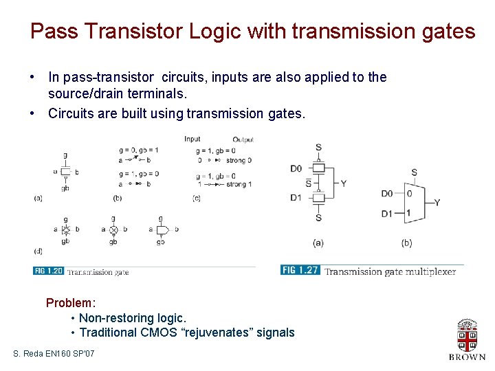
Pass Transistor Logic with transmission gates • In pass-transistor circuits, inputs are also applied to the source/drain terminals. • Circuits are built using transmission gates. Problem: • Non-restoring logic. • Traditional CMOS “rejuvenates” signals S. Reda EN 160 SP’ 07

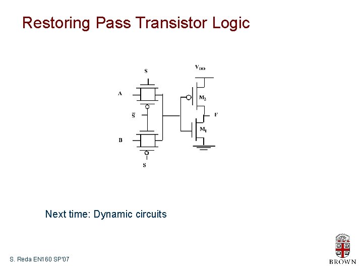
Restoring Pass Transistor Logic Next time: Dynamic circuits S. Reda EN 160 SP’ 07