
Design and commissioning of the ATLAS Muon Spectrometer
- Slides: 35
Design and commissioning of the ATLAS Muon Spectrometer RPC Read Out Driver Vincenzo Izzo Istituto Nazionale di Fisica Nucleare sez. di NAPOLI – ITALY on behalf of the ATLAS collaboration TWEPP 2008 Topical Workshop on Electronics for Particle Physics Naxos (Greece) September 17 th, 2008
Summary • The ATLAS Experiment • The Trigger and Read-out system of the spectrometer • The ROD board architecture • The ROD in the DAQ commissioning • Conclusions 2
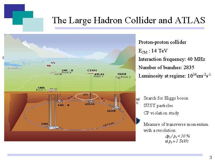
The Large Hadron Collider and ATLAS Proton-proton collider ECM : 14 Te. V Interaction frequency: 40 MHz Number of bunches: 2835 Luminosity at regime: 1034 cm-2 s-1 Search for Higgs boson SUSY particles CP violation study Measure of transverse momentum with a resolution pt / pt < 10 % at pt 1 Te. V/c 3
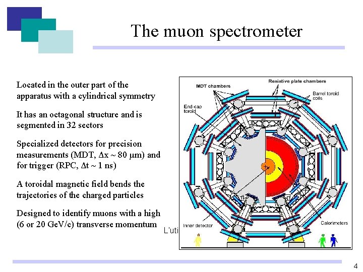
The muon spectrometer Located in the outer part of the apparatus with a cylindrical symmetry It has an octagonal structure and is segmented in 32 sectors Specialized detectors for precision measurements (MDT, Δx ~ 80 µm) and for trigger (RPC, Δt ~ 1 ns) A toroidal magnetic field bends the trajectories of the charged particles Designed to identify muons with a high (6 or 20 Ge. V/c) transverse momentum L’utilizzo di costrutti 4
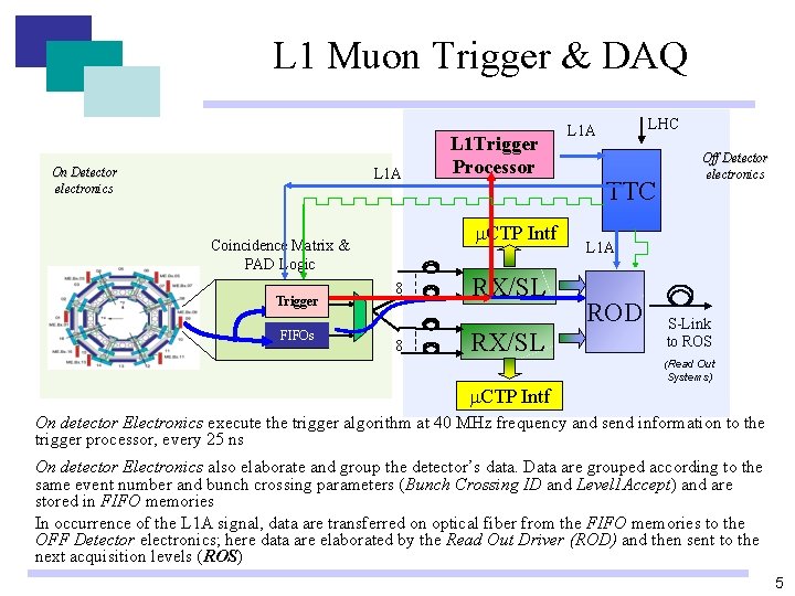
L 1 Muon Trigger & DAQ On Detector electronics L 1 A m. CTP Intf Coincidence Matrix & PAD Logic Trigger FIFOs L 1 Trigger Processor 8 8 RX/SL m. CTP Intf LHC L 1 A TTC Off Detector electronics L 1 A ROD S-Link to ROS (Read Out Systems) On detector Electronics execute the trigger algorithm at 40 MHz frequency and send information to the trigger processor, every 25 ns On detector Electronics also elaborate and group the detector’s data. Data are grouped according to the same event number and bunch crossing parameters (Bunch Crossing ID and Level 1 Accept) and are stored in FIFO memories In occurrence of the L 1 A signal, data are transferred on optical fiber from the FIFO memories to the OFF Detector electronics; here data are elaborated by the Read Out Driver (ROD) and then sent to the next acquisition levels (ROS) 5
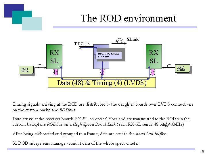
The ROD environment SLink TTC RX SL MUON ROD FRAME L 1 A = xxxx ROD RX SL PAD frame Timing (4) (LVDS) Data (48) & Timing (4) (LVDS) Timing signals arriving at the ROD are distributed to the daughter boards over LVDS connections on the custom backplane RODbus Data arrive at the receiver boards RX-SL on optical fiber and are transmitted to the ROD via the custom backplane RODbus on a High Speed Serial Link (each RX-SL sends 48 bit@40 MHz) After being elaborated and grouped in a frame, data are sent to the Read Out Buffer 32 ROD subsystems manage readout data of the whole spectrometer 6
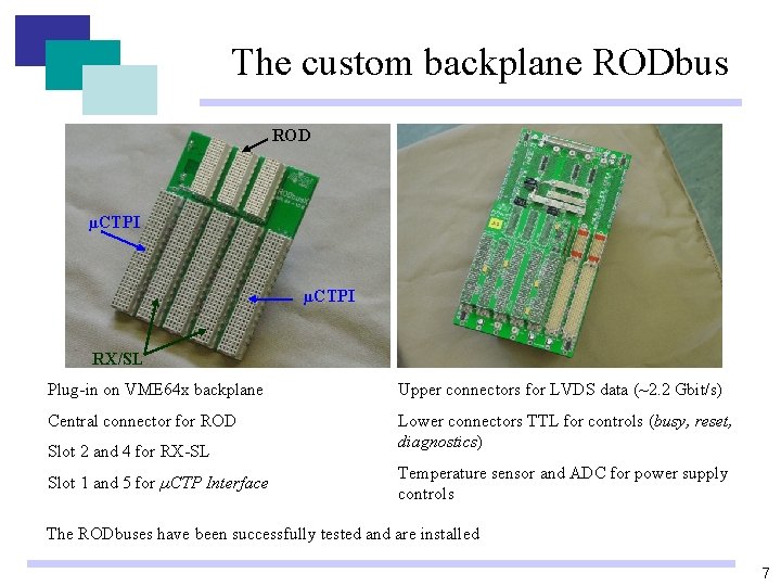
The custom backplane RODbus ROD µCTPI RX/SL Plug-in on VME 64 x backplane Upper connectors for LVDS data (~2. 2 Gbit/s) Central connector for ROD Lower connectors TTL for controls (busy, reset, diagnostics) Slot 2 and 4 for RX-SL Slot 1 and 5 for µCTP Interface Temperature sensor and ADC for power supply controls The RODbuses have been successfully tested and are installed 7
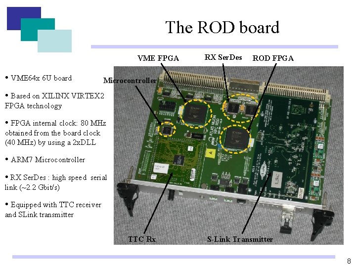
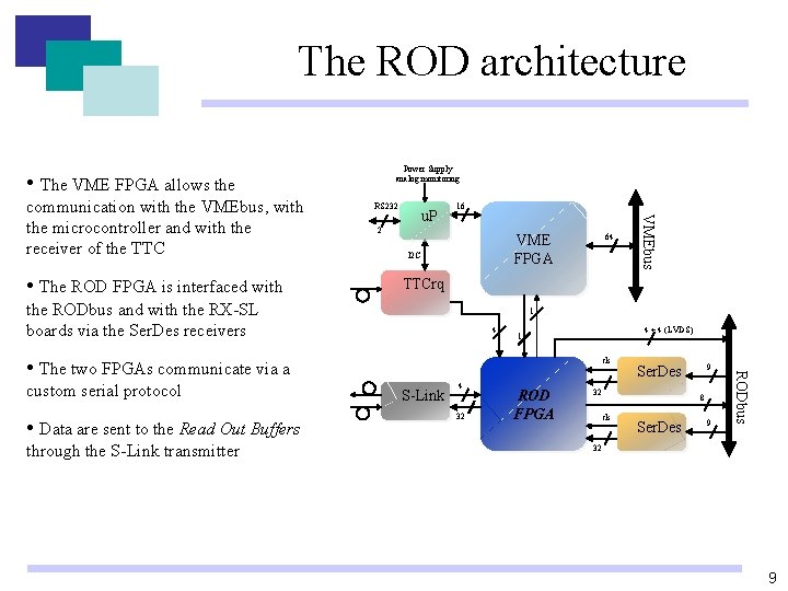
The ROD board VME FPGA • VME 64 x 6 U board RX Ser. Des ROD FPGA Microcontroller • Based on XILINX VIRTEX 2 FPGA technology • FPGA internal clock: 80 MHz obtained from the board clock (40 MHz) by using a 2 x. DLL • ARM 7 Microcontroller • RX Ser. Des : high speed serial link (~2. 2 Gbit/s) • Equipped with TTC receiver and SLink transmitter TTC Rx S-Link Transmitter 8
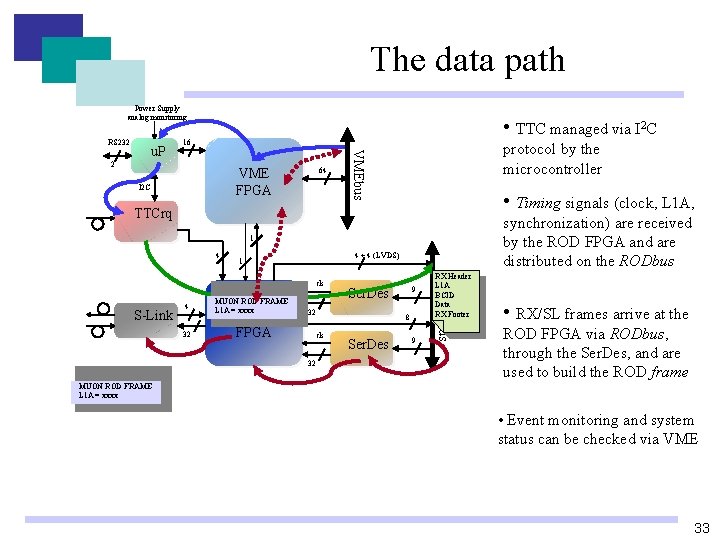
The ROD architecture Power Supply analog monitoring • The VME FPGA allows the • The ROD FPGA is interfaced with RS 232 u. P 16 2 VME FPGA I 2 C 64 TTCrq the RODbus and with the RX-SL boards via the Ser. Des receivers 1 4 4 + 4 (LVDS) 1 • Data are sent to the Read Out Buffers through the S-Link transmitter ck S-Link 4 32 ROD FPGA 9 Ser. Des 32 8 ck Ser. Des 9 RODbus • The two FPGAs communicate via a custom serial protocol VMEbus communication with the VMEbus, with the microcontroller and with the receiver of the TTC 32 9
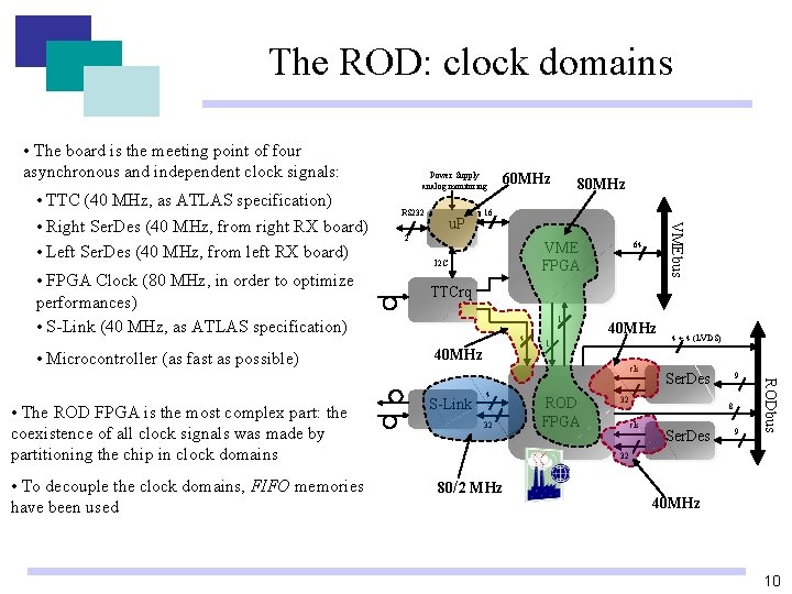
The ROD: clock domains • The board is the meeting point of four asynchronous and independent clock signals: • TTC (40 MHz, as ATLAS specification) • FPGA Clock (80 MHz, in order to optimize performances) • S-Link (40 MHz, as ATLAS specification) • Microcontroller (as fast as possible) • To decouple the clock domains, FIFO memories have been used u. P 80 MHz 16 2 VME FPGA I 2 C 64 TTCrq 1 4 40 MHz 1 ck S-Link 4 32 ROD FPGA 4 + 4 (LVDS) 9 Ser. Des 32 8 ck Ser. Des 9 RODbus • The ROD FPGA is the most complex part: the coexistence of all clock signals was made by partitioning the chip in clock domains RS 232 60 MHz VMEbus • Right Ser. Des (40 MHz, from right RX board) • Left Ser. Des (40 MHz, from left RX board) Power Supply analog monitoring 32 80/2 MHz 40 MHz 10
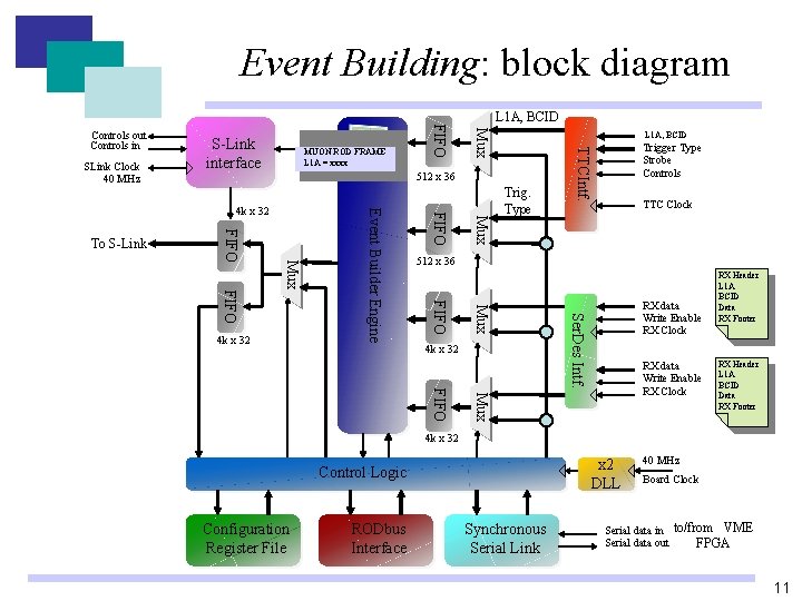
Event Building: block diagram 512 x 36 Mux FIFO Trig. Type TTC Clock 512 x 36 4 k x 32 RX data Write Enable RX Clock Ser. Des Intf. Mux FIFO 4 k x 32 Event Builder Engine 4 k x 32 To S-Link L 1 A, BCID Trigger Type Strobe Controls TTCIntf. MUON ROD FRAME L 1 A = xxxx Mux SLink Clock 40 MHz S-Link interface FIFO Controls out Controls in L 1 A, BCID Mux FIFO RX data Write Enable RX Clock RX Header L 1 A BCID Data RX Footer 4 k x 32 x 2 DLL Control Logic Configuration Register File RODbus Interface Synchronous Serial Link 40 MHz Board Clock Serial data in Serial data out to/from VME FPGA 11
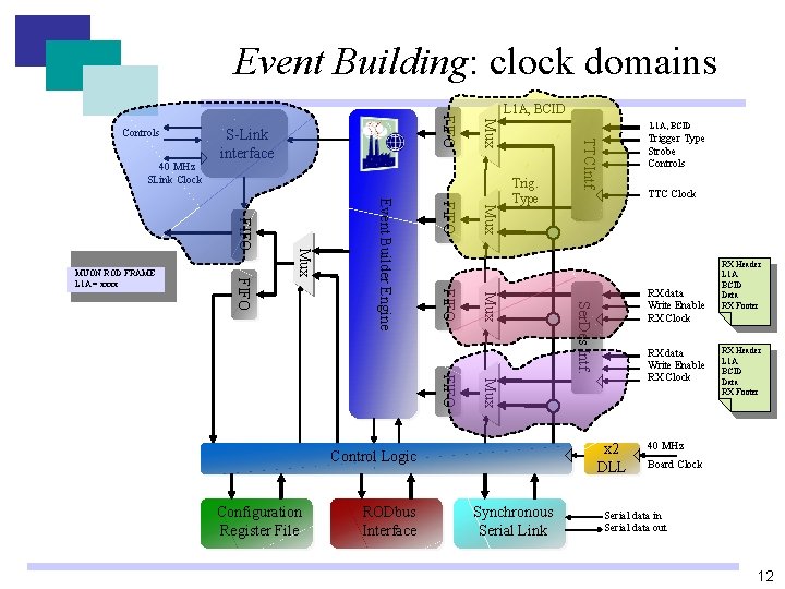
Event Building: clock domains Mux FIFO Trig. Type RX data Write Enable RX Clock Mux FIFO RODbus Interface RX data Write Enable RX Clock x 2 DLL Control Logic Configuration Register File TTC Clock Ser. Des Intf. Mux FIFO Event Builder Engine Mux FIFO MUON ROD FRAME L 1 A = xxxx L 1 A, BCID Trigger Type Strobe Controls TTCIntf. S-Link interface Mux 40 MHz SLink Clock FIFO Controls L 1 A, BCID Synchronous Serial Link RX Header L 1 A BCID Data RX Footer 40 MHz Board Clock Serial data in Serial data out 12
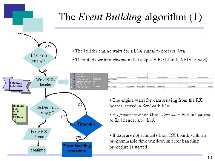
The Event Building algorithm (1) yes • The builder engine waits for a L 1 A signal to process data L 1 A Fifo empty ? • Then starts writing Header in the output FIFO (SLink, VME or both) no ROD Header L 1 A = xxxx RX Header L 1 A BCID Data RX Footer Write ROD header Ser. Des Fifos empty ? no Parse RX frame continue no yes Timeout ? yes Error handling procedure • The engine waits for data arriving from the RX boards, stored in Ser. Des FIFOs • RX frames retrieved from Ser. Des FIFOs are parsed to find header and L 1 A • If data are not available from RX boards within a programmable time window, an error handling procedure is started 13
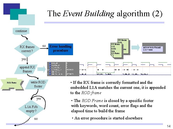
The Event Building algorithm (2) continue no RX frames correct ? Error handling procedure RX Header L 1 A RX Header BCID L 1 A Data BCID RX Footer Data RX Footer MUON ROD FRAME L 1 A = xxxx yes append RX frames ROD Footer write ROD footer yes L 1 A Fifo empty ? no • If the RX frame is correctly formatted and the embedded L 1 A matches the current one, it is appended to the ROD frame • The ROD Frame is closed by a specific footer with keywords, word count, error flags and the elapsed time to build the frame • An error procedure is started elsewhere 14
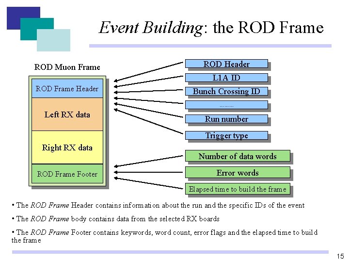
Event Building: the ROD Frame ROD Muon Frame ROD Header L 1 A ID ROD Frame Header Bunch Crossing ID ……… Left RX data Run number Trigger type Right RX data ROD Frame Footer Number of data words Error words Elapsed time to build the frame • The ROD Frame Header contains information about the run and the specific IDs of the event • The ROD Frame body contains data from the selected RX boards • The ROD Frame Footer contains keywords, word count, error flags and the elapsed time to build the frame 15
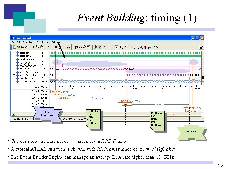
Event Building: timing (1) ROD Header L 1 A = xxxx RX Header L 1 A BCID Data RX Footer ROD Footer • Cursors show the time needed to assembly a ROD Frame • A typical ATLAS situation is shown, with RX Frames made of 80 words@32 bit • The Event Builder Engine can manage an average L 1 A rate higher than 100 KHz 16
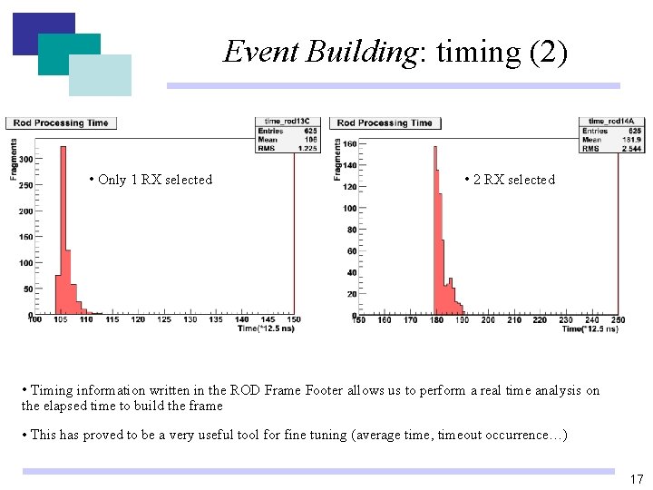
Event Building: timing (2) • Only 1 RX selected • 2 RX selected • Timing information written in the ROD Frame Footer allows us to perform a real time analysis on the elapsed time to build the frame • This has proved to be a very useful tool for fine tuning (average time, timeout occurrence…) 17
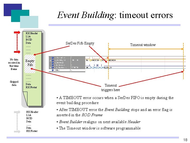
Event Building: timeout errors RX Header L 1 A BCID Data. . . . . No data received in this time frame Skipped data Ser. Des Fifo Empty Timeout window Empty Fifo. . . . . Data RX Footer Timeout triggers here • A TIMEOUT error occurs when a Ser. Des FIFO is empty during the event building procedure RX Header L 1 A BCID Data. . . . Data RX Footer • After TIMEOUT error the Event Building stops and an error flag is asserted in the ROD Frame • Event Builder realigns on next available Header • The Timeout window is software programmable 18
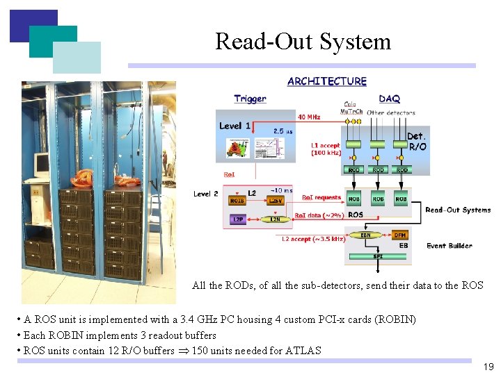
Read-Out System All the RODs, of all the sub-detectors, send their data to the ROS • A ROS unit is implemented with a 3. 4 GHz PC housing 4 custom PCI-x cards (ROBIN) • Each ROBIN implements 3 readout buffers • ROS units contain 12 R/O buffers 150 units needed for ATLAS 19
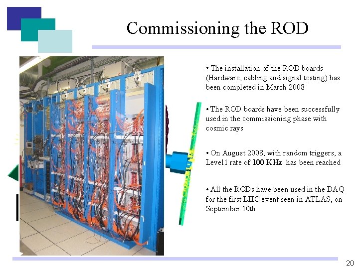
Commissioning the ROD • The installation of the ROD boards (Hardware, cabling and signal testing) has been completed in March 2008 • The ROD boards have been successfully used in the commissioning phase with cosmic rays • On August 2008, with random triggers, a Level 1 rate of 100 KHz has been reached • All the RODs have been used in the DAQ for the first LHC event seen in ATLAS, on September 10 th 20
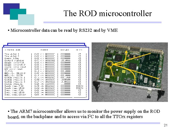
The ROD microcontroller • Microcontroller data can be read by RS 232 and by VME • The ARM 7 microcontroller allows us to monitor the power supply on the ROD board, on the backplane and to access via I 2 C to all the TTCrx registers 21
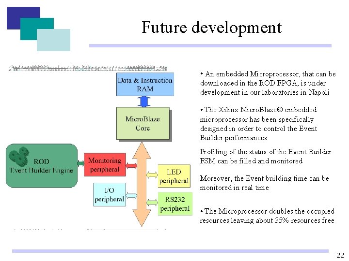
Future development • An embedded Microprocessor, that can be downloaded in the ROD FPGA, is under development in our laboratories in Napoli • The Xilinx Micro. Blaze© embedded microprocessor has been specifically designed in order to control the Event Builder performances Profiling of the status of the Event Builder FSM can be filled and monitored Moreover, the Event building time can be monitored in real time • The Microprocessor doubles the occupied resources leaving about 35% resources free 22
Conclusions We presented the design of the processor that performs the Event Building of data of the RPC detectors of the muon spectrometer The board architecture and some of the board features have been presented The project was not limited to the design of a single board. Instead we built a whole environment and we are presently taking care of its integration in the ATLAS DAQ system All the Read Out Driver boards have been installed in the ATLAS DAQ system and have been successfully used in the ATLAS DAQ commissioning phase New monitoring features, based on Xilinx Micro. Blaze© embedded microprocessor, are presently being developed 23
24
Backup slides 25
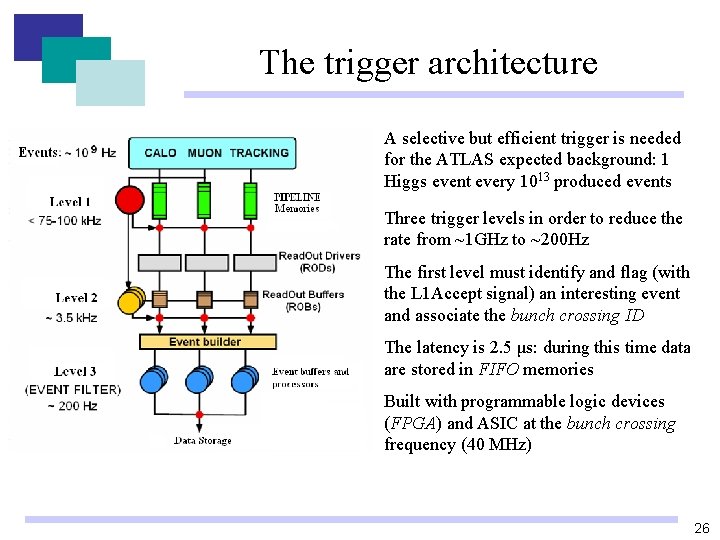
The trigger architecture A selective but efficient trigger is needed for the ATLAS expected background: 1 Higgs event every 1013 produced events Three trigger levels in order to reduce the rate from ~1 GHz to ~200 Hz The first level must identify and flag (with the L 1 Accept signal) an interesting event and associate the bunch crossing ID The latency is 2. 5 μs: during this time data are stored in FIFO memories Built with programmable logic devices (FPGA) and ASIC at the bunch crossing frequency (40 MHz) 26
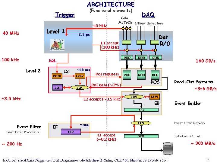
ARCHITECTURE (Functional elements) Trigger 40 MHz Level 1 40 MHz DAQ Calo Mu. Tr. Ch Other detectors 2. 5 ms Det. R/O L 1 accept (100 k. Hz) 100 k. Hz Ro. I Level 2 ROIB L 2 ~10 ms L 2 SV ~3. 5 k. Hz ROD ROB ROB ROS Ro. I data (~2%) L 2 N L 2 P Ro. I requests ROD L 2 accept (~3. 5 k. Hz) 160 GB/s Read-Out Systems ~3+6 GB/s DFM EBN EB Event Builder SFI Event Filter Processors ~ 200 Hz ~ sec EF EFP EF accept (~0. 2 k. Hz) EFN Event Filter Network SFO Sub-Farm Output B. Gorini, The ATLAS Trigger and Data Acquisition - Architecture & Status, CHEP 06, Mumbai 13 -19 Feb. 2006 ~ 300 MB/s 27
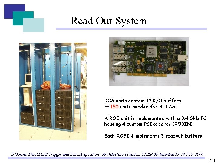
Read Out System ROS units contain 12 R/O buffers 150 units needed for ATLAS A ROS unit is implemented with a 3. 4 GHz PC housing 4 custom PCI-x cards (ROBIN) Each ROBIN implements 3 readout buffers B. Gorini, The ATLAS Trigger and Data Acquisition - Architecture & Status, CHEP 06, Mumbai 13 -19 Feb. 2006 28
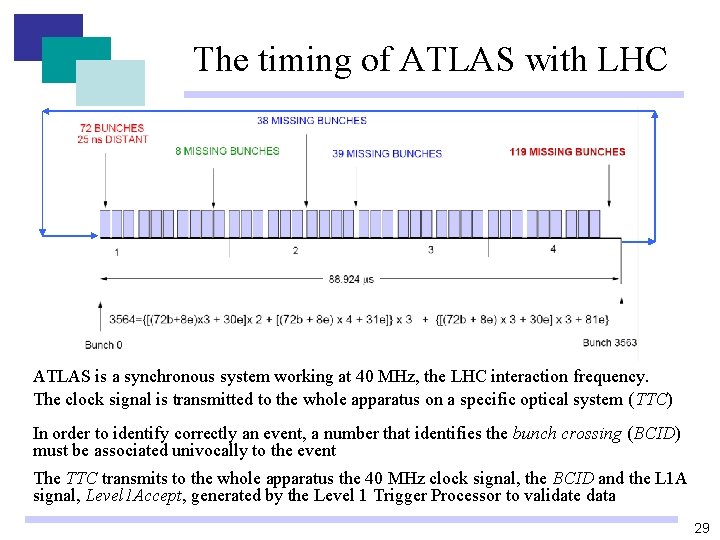
The timing of ATLAS with LHC ATLAS is a synchronous system working at 40 MHz, the LHC interaction frequency. The clock signal is transmitted to the whole apparatus on a specific optical system (TTC) In order to identify correctly an event, a number that identifies the bunch crossing (BCID) must be associated univocally to the event The TTC transmits to the whole apparatus the 40 MHz clock signal, the BCID and the L 1 A signal, Level 1 Accept, generated by the Level 1 Trigger Processor to validate data 29
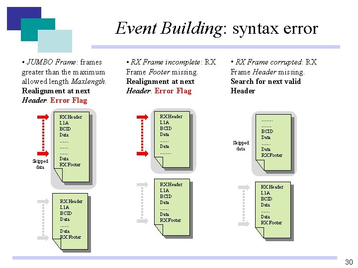
Event Building: syntax error • JUMBO Frame: frames greater than the maximum allowed length Maxlength. Realignment at next Header. Error Flag Skipped data RX Header L 1 A BCID Data. . . . . Data RX Footer RX Header L 1 A BCID Data. . . . Data RX Footer • RX Frame incomplete: RX Frame Footer missing. Realignment at next Header. Error Flag RX Header L 1 A BCID Data. . . . Data RX Footer • RX Frame corrupted: RX Frame Header missing. Search for next valid Header Skipped data . . . . BCID Data. . . . Data RX Footer RX Header L 1 A BCID Data. . . . Data RX Footer 30
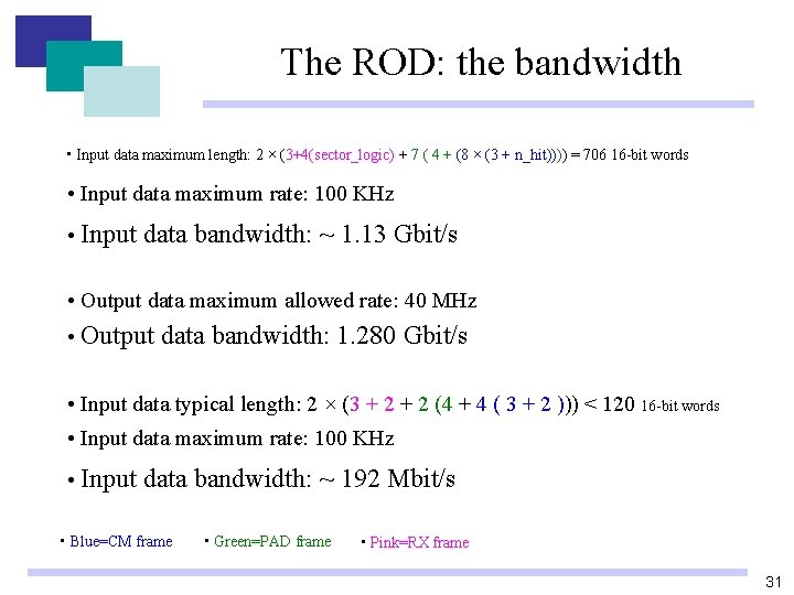
The ROD: the bandwidth • Input data maximum length: 2 × (3+4(sector_logic) + 7 ( 4 + (8 × (3 + n_hit)))) = 706 16 -bit words • Input data maximum rate: 100 KHz • Input data bandwidth: ~ 1. 13 Gbit/s • Output data maximum allowed rate: 40 MHz • Output data bandwidth: 1. 280 Gbit/s • Input data typical length: 2 × (3 + 2 (4 + 4 ( 3 + 2 ))) < 120 16 -bit words • Input data maximum rate: 100 KHz • Input data bandwidth: ~ 192 Mbit/s • Blue=CM frame • Green=PAD frame • Pink=RX frame 31
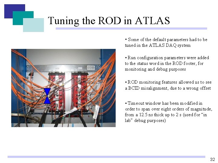
Tuning the ROD in ATLAS • Some of the default parameters had to be tuned in the ATLAS DAQ system • Run configuration parameters were added to the status word in the ROD footer, for monitoring and debug purposes • ROD monitoring features allowed us to see a BCID misalignment, due to a wrong offset • Timeout window has been modified in order to span over eight orders of magnitude, from a 12. 5 ns thick up to 2 s (used for “in lab” debug purposes) 32
The data path Power Supply analog monitoring RS 232 16 2 VME FPGA I 2 C 64 protocol by the microcontroller VMEbus u. P • TTC managed via I 2 C • Timing signals (clock, L 1 A, TTCrq synchronization) are received by the ROD FPGA and are distributed on the RODbus 1 4 4 + 4 (LVDS) 1 ck 4 32 ROD FPGA 32 8 ck 32 9 Ser. Des 9 RODbus S-Link MUON ROD FRAME L 1 A = xxxx RX Header L 1 A BCID Data RX Footer • RX/SL frames arrive at the ROD FPGA via RODbus, through the Ser. Des, and are used to build the ROD frame MUON ROD FRAME L 1 A = xxxx • Event monitoring and system status can be checked via VME 33
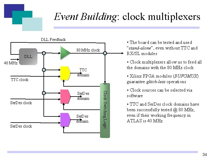
Event Building: clock multiplexers DLL Feedback • The board can be tested and used “stand-alone”, even without TTC and RX/SL modules 80 MHz clock DLL • Clock multiplexers allow us to feed all the domains with the 80 MHz clock 40 MHz TTC domain • Xilinx FPGA modules (BUFGMUX) guarantee glitch-less operations TTC clock Ser. Des domain Ser. Des clock Clock Switching Logic Ser. Des domain • Clock sources can be selected via software • TTC and Ser. Des clock domains have been successfully tested @ 80 MHz, even if their working frequency in ATLAS is 40 MHz 34
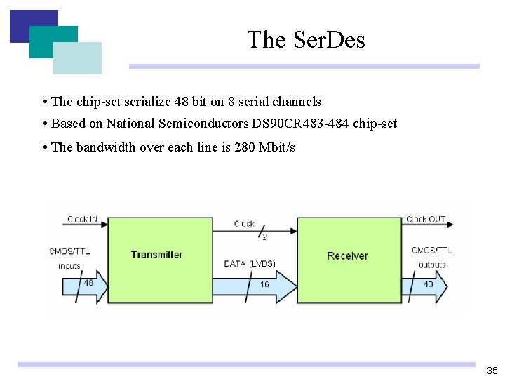
The Ser. Des • The chip-set serialize 48 bit on 8 serial channels • Based on National Semiconductors DS 90 CR 483 -484 chip-set • The bandwidth over each line is 280 Mbit/s 35