
Design and Assessment of a Robust Voltage Amplifier
Design and Assessment of a Robust Voltage Amplifier with 2. 5 GHz GBW and >100 k. Gy Total Dose Tolerance Jens Verbeeck TWEPP 2010
Outline = Introduction = Radiation and temperature effects = Constant gm amplifier = Matching structure = Conclusions Presentation: Jens Verbeeck 2
Outline = Introduction = Radiation and temperature effects = Constant gm amplifier = Matching structure = Conclusions Presentation: Jens Verbeeck 3
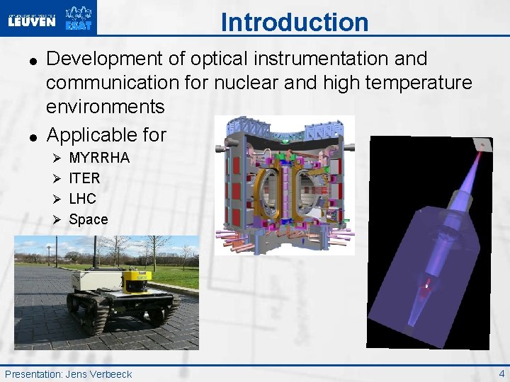
Introduction = = Development of optical instrumentation and communication for nuclear and high temperature environments Applicable for Ø MYRRHA Ø ITER Ø LHC Ø Space Presentation: Jens Verbeeck 4

Optical instrumentation PD: Photo diode AGC: Automatic gain controller TIA: Transimpedance amplifier TDC: Time to digital converter LA: Limiting amplifier Presentation: Jens Verbeeck 5
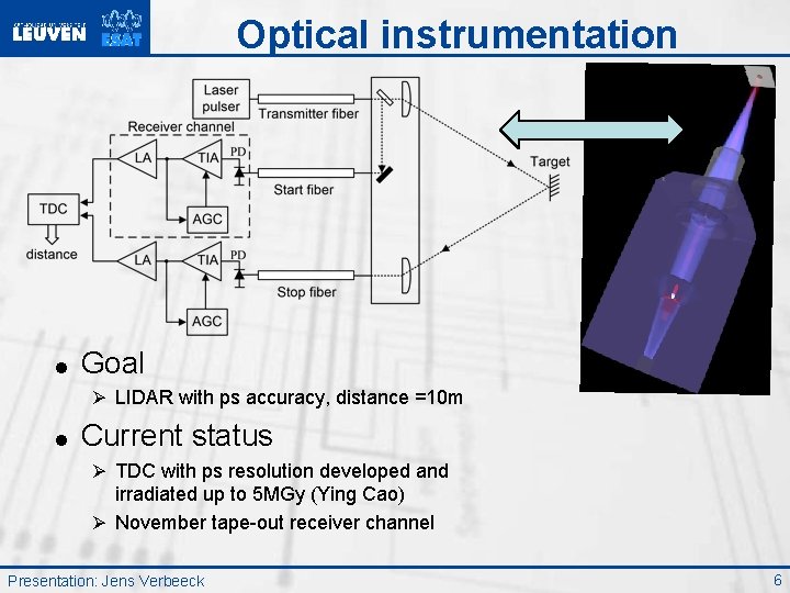
Optical instrumentation = Goal Ø LIDAR with ps accuracy, distance =10 m = Current status Ø TDC with ps resolution developed and irradiated up to 5 MGy (Ying Cao) Ø November tape-out receiver channel Presentation: Jens Verbeeck 6
Outline = Introduction = Radiation and temperature effects = Constant gm amplifier = Matching as a function of radiation dose = Conclusions Presentation: Jens Verbeeck 7
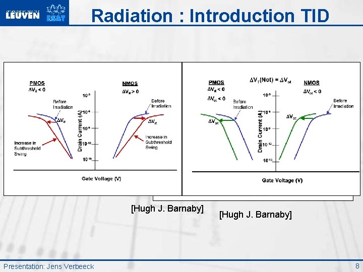
Radiation : Introduction TID Oxide: Net positive charge trapped at the oxide Si-Si. O 2 interface: vg > 0 => +∆vth (NMOS) vg < 0 => -∆vth (PMOS) [Hugh J. Barnaby] Presentation: Jens Verbeeck [Hugh J. Barnaby] 8
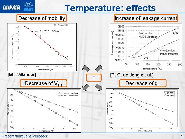
Temperature: effects Decrease of mobility [M. Willander] Decrease of VTH Presentation: Jens Verbeeck Increase of leakage current T [P. C. de Jong et. al. ] Decrease of gm 9
Outline = Introduction = Radiation and temperature effects = Constant gm amplifier = Matching as structure = Conclusions Presentation: Jens Verbeeck 10
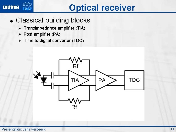
Optical receiver = Classical building blocks Ø Transimpedance amplifier (TIA) Ø Post amplifier (PA) Ø Time to digital convertor (TDC) Presentation: Jens Verbeeck 11

Constant gm amplifier: Why? Radiation/temperature causes variation in TIA parameters Ø gm and rout variable in formula A 0 § Make gain independent of gm and rout Presentation: Jens Verbeeck 12

Constant gm amplifier: Why? Radiation up to 300 k. Gy (M. Manghisoni et al. ) 0. 18µm 100 k. Gy 300 k. Gy CMOS NMOS +7 m. V +20 m. V PMOS -12 m. V -60 m. V Temperature (-40 up to 130°C) Presentation: Jens Verbeeck 13

Constant gm amplifier: Operation [B. Razavi] [Sean Nicalson et al. ] Presentation: Jens Verbeeck = RDSTOT >> RL Ø Transistor length ↑ Ø Trade-off: BB <=> temp/RAD tolerance 14
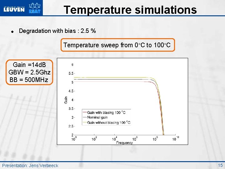
Temperature simulations = Degradation with bias : 2. 5 % Temperature sweep from 0°C to 100°C Gain =14 d. B GBW = 2. 5 Ghz BB = 500 MHz Presentation: Jens Verbeeck 15
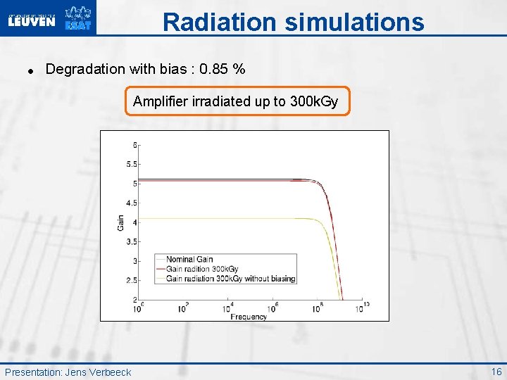
Radiation simulations = Degradation with bias : 0. 85 % Amplifier irradiated up to 300 k. Gy Presentation: Jens Verbeeck 16
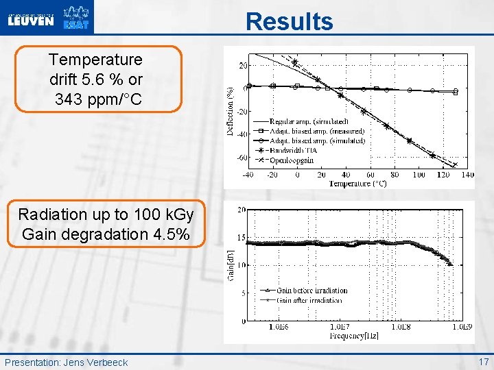
Results Temperature drift 5. 6 % or 343 ppm/°C Radiation up to 100 k. Gy Gain degradation 4. 5% Presentation: Jens Verbeeck 17
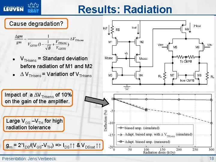
Results: Radiation Cause degradation? = = VTHsens = Standard deviation before radiation of M 1 and M 2 ∆ VTHsens = Variation of VTHsens Impact of a ∆VTHsens of 10% on the gain of the amplifier. Large VGS –VTH for high radiation tolerance gm = 2*IDS/(VGS-VTH) => IDS↑↑ & VDSsat ↑↑ Presentation: Jens Verbeeck 18
Layout Presentation: Jens Verbeeck 19
Outline = Introduction = Radiation and temperature effects = Constant gm amplifier = Matching structure = Conclusions Presentation: Jens Verbeeck 20
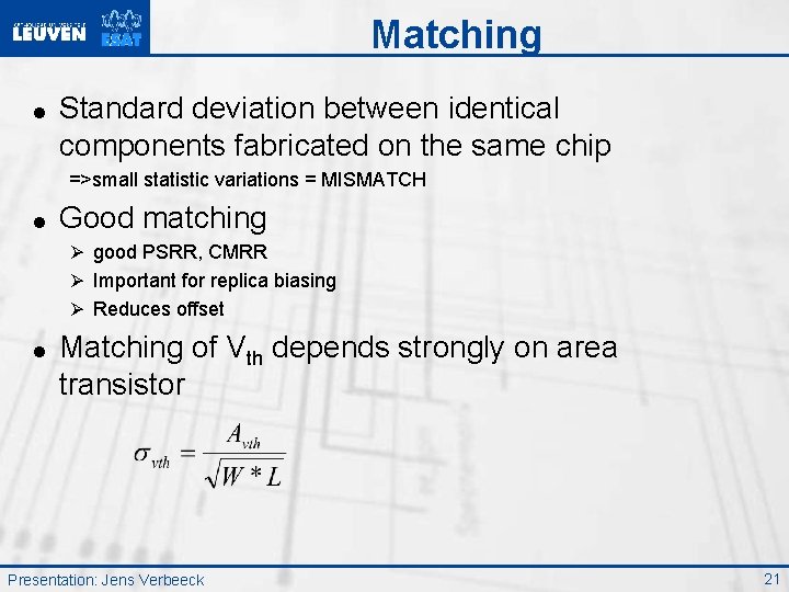
Matching = Standard deviation between identical components fabricated on the same chip =>small statistic variations = MISMATCH = Good matching Ø good PSRR, CMRR Ø Important for replica biasing Ø Reduces offset = Matching of Vth depends strongly on area transistor Presentation: Jens Verbeeck 21
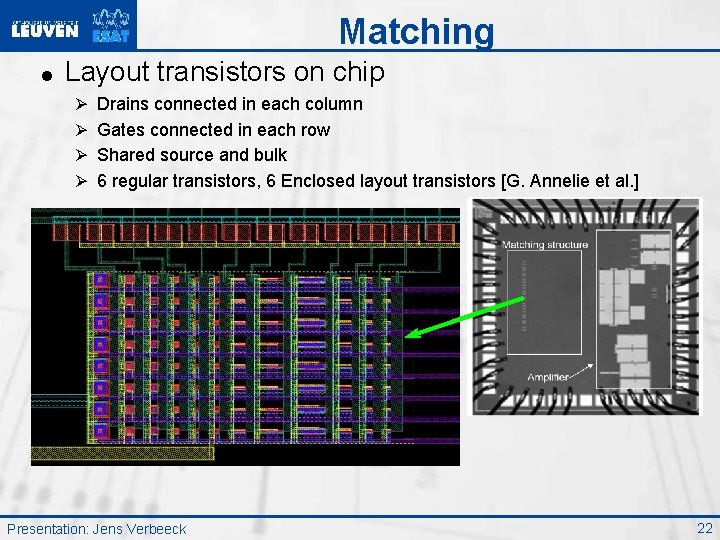
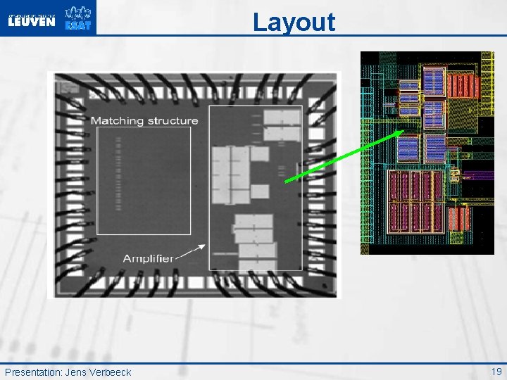
Matching = Layout transistors on chip Ø Drains connected in each column Ø Gates connected in each row Ø Shared source and bulk Ø 6 regular transistors, 6 Enclosed layout transistors [G. Annelie et al. ] Presentation: Jens Verbeeck 22
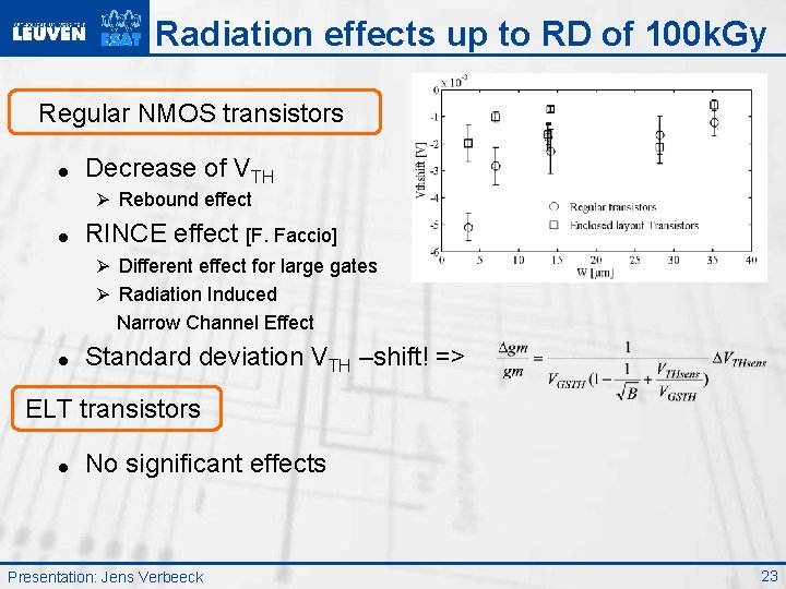
Radiation effects up to RD of 100 k. Gy Regular NMOS transistors = Decrease of VTH Ø Rebound effect = RINCE effect [F. Faccio] Ø Different effect for large gates Ø Radiation Induced Narrow Channel Effect = Standard deviation VTH –shift! => ELT transistors = No significant effects Presentation: Jens Verbeeck 23
Outline = Introduction = Radiation and temperature effects = Constant gm amplifier = Transistor measurements = Conclusions Presentation: Jens Verbeeck 24
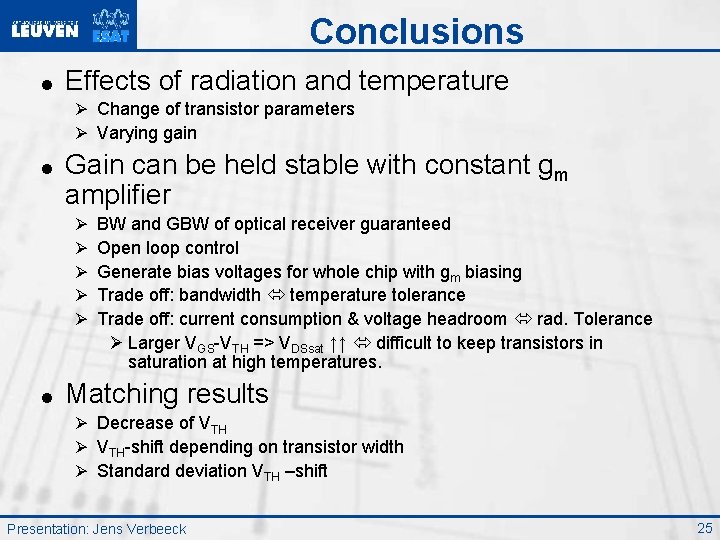
Conclusions = Effects of radiation and temperature Ø Change of transistor parameters Ø Varying gain = Gain can be held stable with constant gm amplifier Ø Ø Ø = BW and GBW of optical receiver guaranteed Open loop control Generate bias voltages for whole chip with gm biasing Trade off: bandwidth temperature tolerance Trade off: current consumption & voltage headroom rad. Tolerance Ø Larger VGS-VTH => VDSsat ↑↑ difficult to keep transistors in saturation at high temperatures. Matching results Ø Decrease of VTH Ø VTH-shift depending on transistor width Ø Standard deviation VTH –shift Presentation: Jens Verbeeck 25
Questions Acknowledgments to: Presentation: Jens Verbeeck ? 26
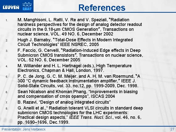
References 1. 2. 3. 4. 5. 6. 7. 8. M. Manghisoni, L. Ratti, V. Re and V. Speziali, “Radiation hardness perspectives for the design of analog detector readout circuits in the 0. 18 -µm CMOS Generation”, Transactions on nuclear science, VOL. 49 NO. 6, December 2002 Hugh J. Barnaby, “Total-Dose Effects in Modern Integrated Circuit Technologies” IEEE NSREC, 2005 F. Faccio, G. Cervelli, “Radiation-Induced Edge effects in Deep Submicron CMOS transistors”, Transactions on nuclear science, VOL. 52 NO. 6, December 2005 M. Willander and H. L. Hartnagel (eds. ), High Temperature Electronics, Chapman & Hall, London, 1997. P. C. de Jong, G. C. M. Meijer, and A. H. M. van Roermund, “A 300 °C dynamic feedback instrumentation amplifier, ” IEEE J. Solid-State Circuits, vol. 33, no. 12, pp. 1999 -2009, Dec. 1998. Sean Nicalson and Khoman Phang, “Improvements in biasing and compensation of cmos opamps”, ISCAS 2004 B. Razavi, “Design of analog integrated circuits” G. Anelli et al. , “ Radiation tolerant VLSI circuits in standard deep submicron CMOS technologies for the LHC experiments: Practical design aspects, ” IEEE Trans. Nucl. Sci. , vol. 46, no. 6, pp. 1690– 1696, Dec. 1999. Presentation: Jens Verbeeck 27
- Slides: 27