DEPT OF MODERN PHYSICS USTC Electronics System of

- Slides: 36

DEPT OF MODERN PHYSICS, USTC Electronics System of MC 2002. 6. 5 IHEP, Beijing ______________________ Muon Group, USTC, Hefei

DEPT OF MODERN PHYSICS, USTC CONTENTS Overview of structure Readout System of MC Test System of MC

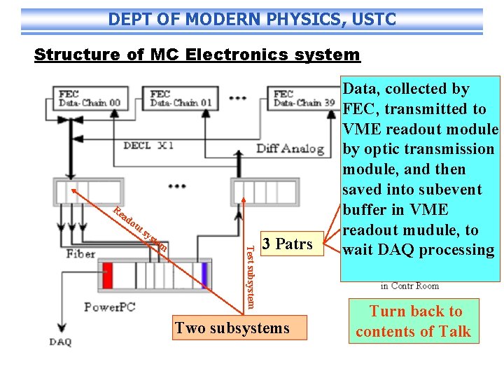
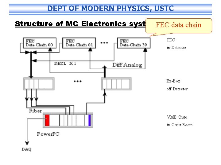
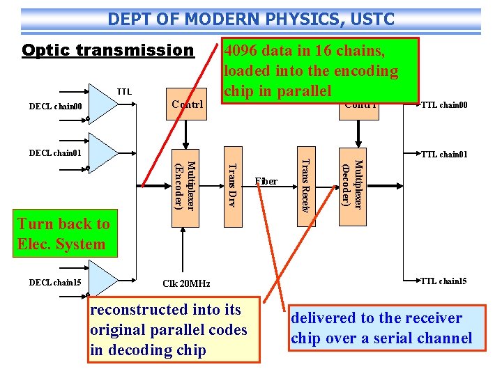
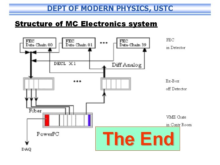
DEPT OF MODERN PHYSICS, USTC Structure of MC Electronics system Re a do ut s ys Test subsystem 3 Patrs Two subsystems Data, collected by FEC, transmitted to VME readout module by optic transmission module, and then saved into subevent buffer in VME readout mudule, to wait DAQ processing Turn back to contents of Talk

DEPT OF MODERN PHYSICS, USTC CONTENTS Overview of structure Readout System of MC Test System of MC

DEPT OF MODERN PHYSICS, USTC Structure of MC Electronics system. FEC data chain

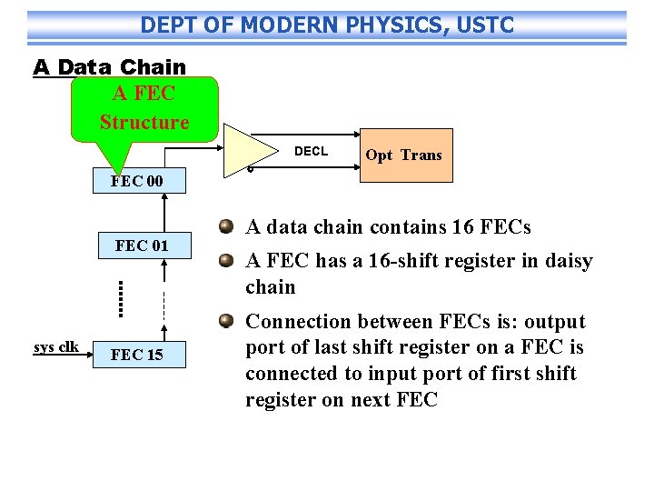
DEPT OF MODERN PHYSICS, USTC A Data Chain A FEC Structure DECL Opt Trans FEC 00 FEC 01 sys clk FEC 15 A data chain contains 16 FECs A FEC has a 16 -shift register in daisy chain Connection between FECs is: output port of last shift register on a FEC is connected to input port of first shift register on next FEC

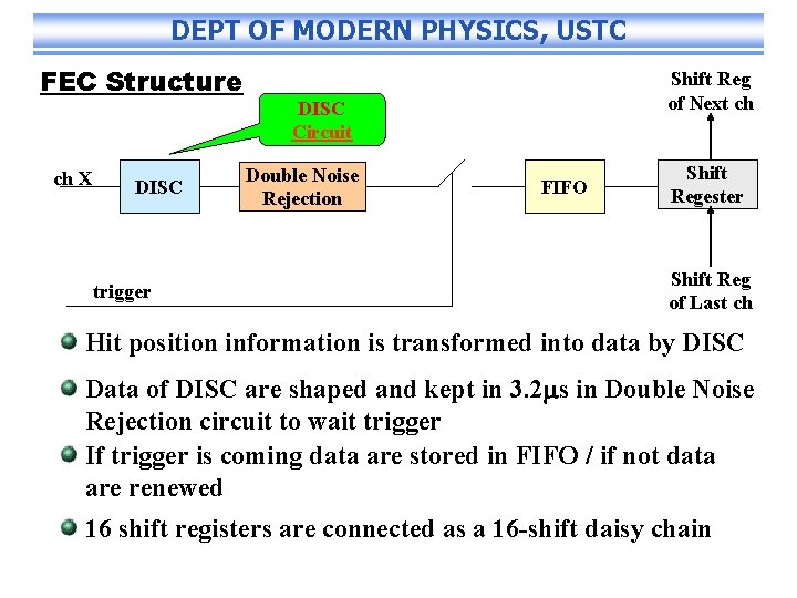
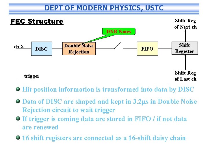
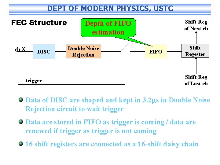
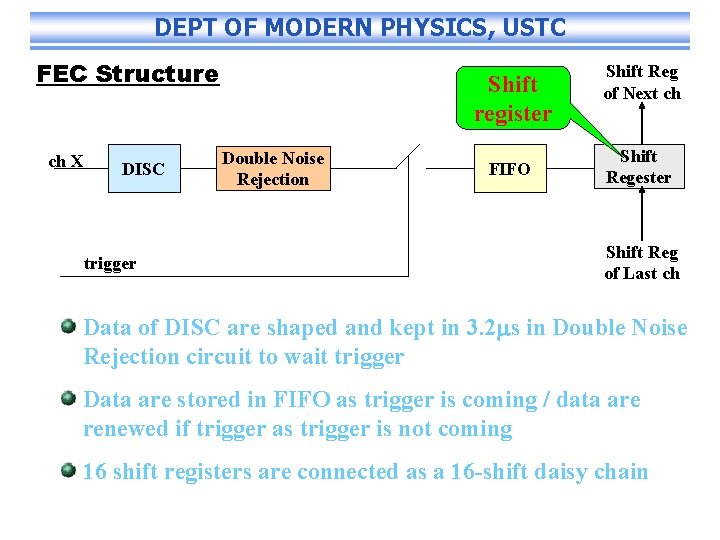
DEPT OF MODERN PHYSICS, USTC FEC Structure ch X DISC trigger Shift Reg of Next ch DISC Circuit Double Noise Rejection FIFO Shift Regester Shift Reg of Last ch Hit position information is transformed into data by DISC Data of DISC are shaped and kept in 3. 2 s in Double Noise Rejection circuit to wait trigger If trigger is coming data are stored in FIFO / if not data are renewed 16 shift registers are connected as a 16 -shift daisy chain

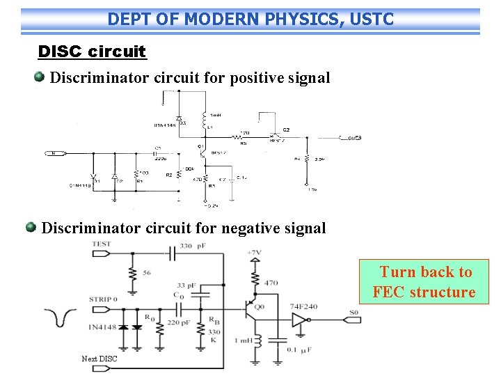
DEPT OF MODERN PHYSICS, USTC DISC circuit Discriminator circuit for positive signal Discriminator circuit for negative signal Turn back to FEC structure

DEPT OF MODERN PHYSICS, USTC FEC Structure Shift Reg of Next ch DNR Notes ch X DISC trigger Double Noise Rejection FIFO Shift Regester Shift Reg of Last ch Hit position information is transformed into data by DISC Data of DISC are shaped and kept in 3. 2 s in Double Noise Rejection circuit to wait trigger If trigger is coming data are stored in FIFO / if not data are renewed 16 shift registers are connected as a 16 -shift daisy chain

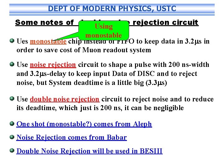
DEPT OF MODERN PHYSICS, USTC Some notes of double noise rejection circuit Using monostable Ues monostable chip instead of FIFO to keep data in 3. 2 s in order to save cost of Muon readout system Use noise rejection circuit to shape a pulse with 200 ns-width and 3. 2 s-delay to keep input Data of DISC and to reject noise, but System deadtime is a little big (3. 3 s) Use double noise rejection circuit to reject noise and to reduce its deadtime, which just is 200 ns, it can be negligible One shot (monostable? ) comes from Aleph Noise Rejection comes from Babar Double Noise Rejection will be used in BESIII

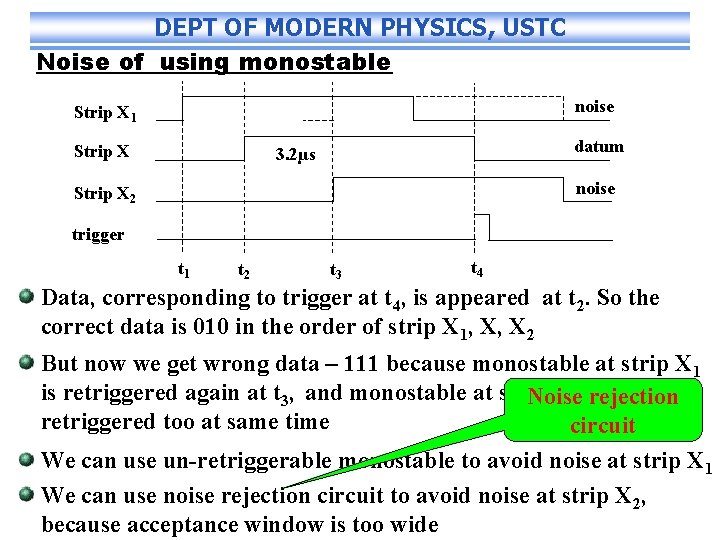
DEPT OF MODERN PHYSICS, USTC Noise of using monostable noise Strip X 1 Strip X datum 3. 2µs noise Strip X 2 trigger t 1 t 2 t 3 t 4 Data, corresponding to trigger at t 4, is appeared at t 2. So the correct data is 010 in the order of strip X 1, X, X 2 But now we get wrong data – 111 because monostable at strip X 1 is retriggered again at t 3, and monostable at strip X 2 isrejection Noise retriggered too at same time circuit We can use un-retriggerable monostable to avoid noise at strip X 1 We can use noise rejection circuit to avoid noise at strip X 2, because acceptance window is too wide

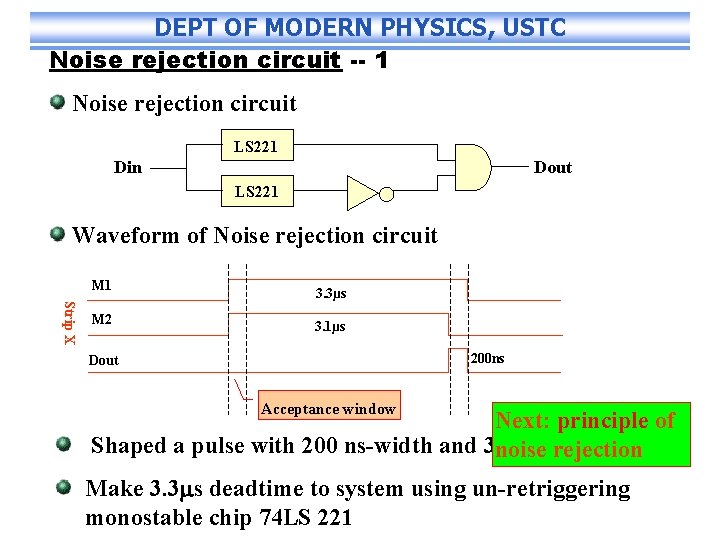
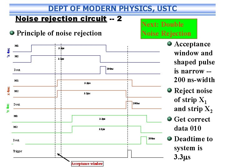
DEPT OF MODERN PHYSICS, USTC Noise rejection circuit -- 1 Noise rejection circuit LS 221 Din Dout LS 221 Waveform of Noise rejection circuit M 1 Strip X M 2 3. 3µs 3. 1µs 200 ns Dout Acceptance window Next: principle of Shaped a pulse with 200 ns-width and 3. 2 s-delay noise rejection Make 3. 3 s deadtime to system using un-retriggering monostable chip 74 LS 221

DEPT OF MODERN PHYSICS, USTC Noise rejection circuit -- 2 Next: Double Principle of noise rejection Noise Rejection Acceptance window and shaped pulse Dout is narrow -200 ns-width Reject noise of strip X 1 Dout and strip X 2 Get correct data 010 Dout Deadtime to system is Trigger 3. 3 s M 1 Strip X 1 M 2 3. 3µs 3. 1µs 200 ns M 1 Strip X M 2 3. 3µs 3. 1µs Strip X 2 200 ns M 1 M 2 3. 3µs 3. 1µs 200 ns Acceptance window

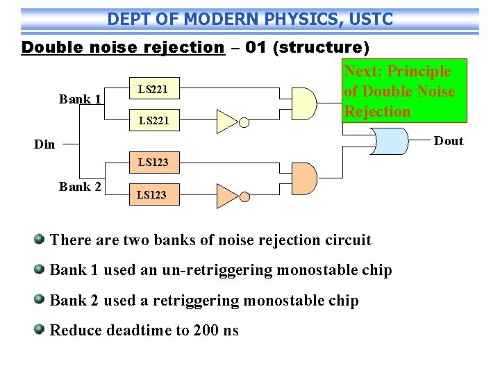
DEPT OF MODERN PHYSICS, USTC Double noise rejection – 01 (structure) Next: Principle LS 221 of Double Noise Bank 1 Rejection LS 221 Dout Din LS 123 Bank 2 LS 123 There are two banks of noise rejection circuit Bank 1 used an un-retriggering monostable chip Bank 2 used a retriggering monostable chip Reduce deadtime to 200 ns

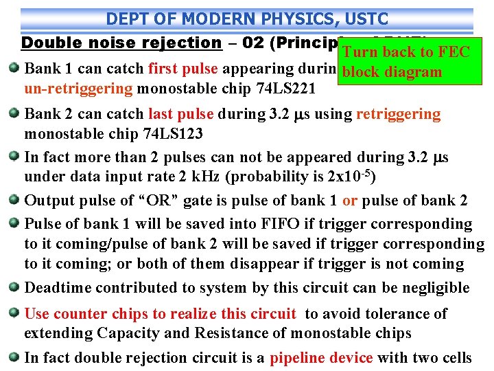
DEPT OF MODERN PHYSICS, USTC Double noise rejection – 02 (Principle of DNR) Turn back to FEC Bank 1 can catch first pulse appearing duringblock 3. 2 sdiagram using un-retriggering monostable chip 74 LS 221 Bank 2 can catch last pulse during 3. 2 s using retriggering monostable chip 74 LS 123 In fact more than 2 pulses can not be appeared during 3. 2 s under data input rate 2 k. Hz (probability is 2 x 10 -5) Output pulse of “OR” gate is pulse of bank 1 or pulse of bank 2 Pulse of bank 1 will be saved into FIFO if trigger corresponding to it coming/pulse of bank 2 will be saved if trigger corresponding to it coming; or both of them disappear if trigger is not coming Deadtime contributed to system by this circuit can be negligible Use counter chips to realize this circuit to avoid tolerance of extending Capacity and Resistance of monostable chips In fact double rejection circuit is a pipeline device with two cells

DEPT OF MODERN PHYSICS, USTC FEC Structure ch X DISC trigger Shift Reg of Next ch Depth of FIFO estimation Double Noise Rejection FIFO Shift Regester Shift Reg of Last ch Data of DISC are shaped and kept in 3. 2 s in Double Noise Rejection circuit to wait trigger Data are stored in FIFO as trigger is coming / data are renewed if trigger as trigger is not coming 16 shift registers are connected as a 16 -shift daisy chain

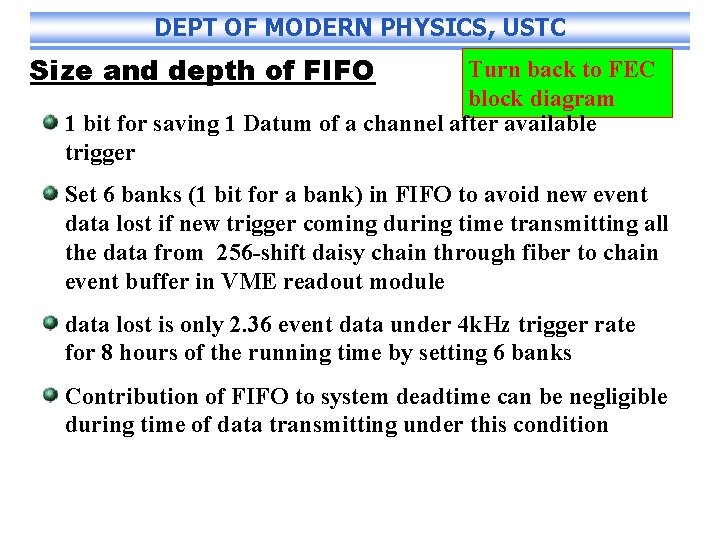
DEPT OF MODERN PHYSICS, USTC Size and depth of FIFO Turn back to FEC block diagram 1 bit for saving 1 Datum of a channel after available trigger Set 6 banks (1 bit for a bank) in FIFO to avoid new event data lost if new trigger coming during time transmitting all the data from 256 -shift daisy chain through fiber to chain event buffer in VME readout module data lost is only 2. 36 event data under 4 k. Hz trigger rate for 8 hours of the running time by setting 6 banks Contribution of FIFO to system deadtime can be negligible during time of data transmitting under this condition

DEPT OF MODERN PHYSICS, USTC FEC Structure ch X DISC trigger Shift register Double Noise Rejection FIFO Shift Reg of Next ch Shift Regester Shift Reg of Last ch Data of DISC are shaped and kept in 3. 2 s in Double Noise Rejection circuit to wait trigger Data are stored in FIFO as trigger is coming / data are renewed if trigger as trigger is not coming 16 shift registers are connected as a 16 -shift daisy chain

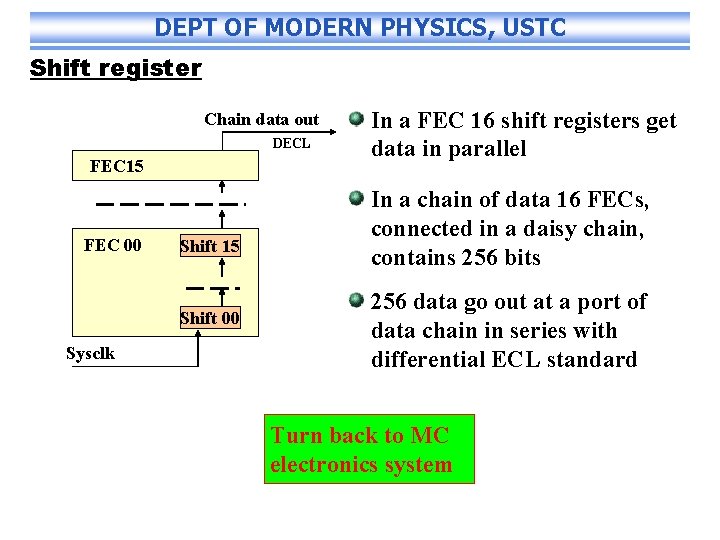
DEPT OF MODERN PHYSICS, USTC Shift register Chain data out DECL FEC 15 FEC 00 Shift 15 Shift 00 Sysclk In a FEC 16 shift registers get data in parallel In a chain of data 16 FECs, connected in a daisy chain, contains 256 bits 256 data go out at a port of data chain in series with differential ECL standard Turn back to MC electronics system

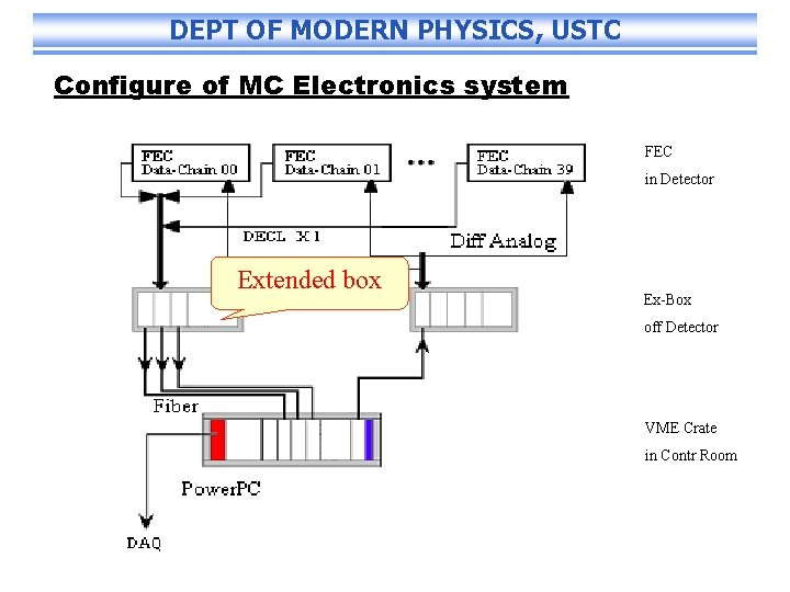
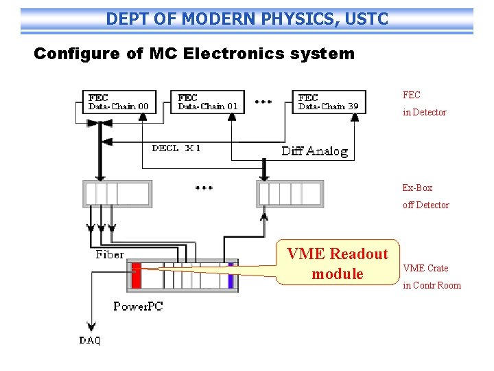
DEPT OF MODERN PHYSICS, USTC Configure of MC Electronics system FEC in Detector Extended box Ex-Box off Detector VME Crate in Contr Room

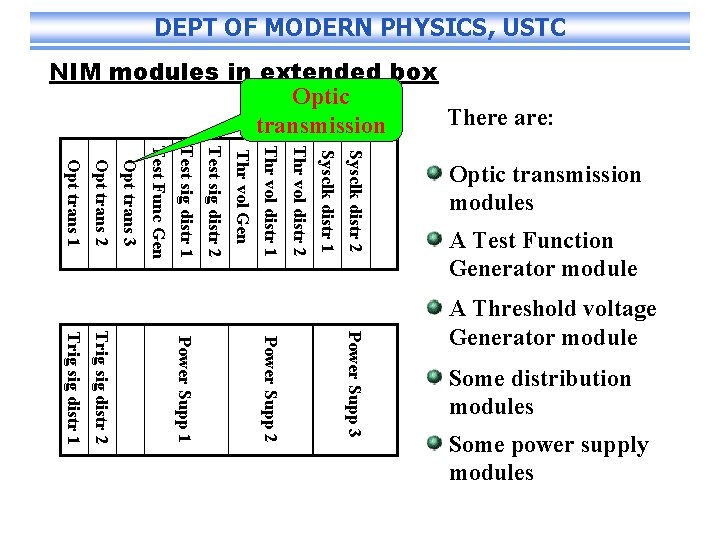
DEPT OF MODERN PHYSICS, USTC NIM modules in extended box Optic There are: transmission Sysclk distr 2 Sysclk distr 1 Thr vol distr 2 Thr vol distr 1 Thr vol Gen Test sig distr 2 Test sig distr 1 Test Func Gen Opt trans 3 Opt trans 2 Opt trans 1 Optic transmission modules A Test Function Generator module Power Supp 3 Power Supp 2 Power Supp 1 Trig sig distr 2 Trig sig distr 1 A Threshold voltage Generator module Some distribution modules Some power supply modules

DEPT OF MODERN PHYSICS, USTC Optic transmission TTL Contrl DECL chain 00 4096 data in 16 chains, loaded into the encoding chip in parallel Contrl DECL chain 01 TTL chain 01 Multiplexer (Decoder) Trans Receiv Trans Drv Multiplexer (Encoder) Fiber TTL chain 00 Turn back to Elec. System DECL chain 15 Clk 20 MHz reconstructed into its original parallel codes in decoding chip TTL chain 15 delivered to the receiver chip over a serial channel

DEPT OF MODERN PHYSICS, USTC Configure of MC Electronics system FEC in Detector Ex-Box off Detector VME Readout module VME Crate in Contr Room

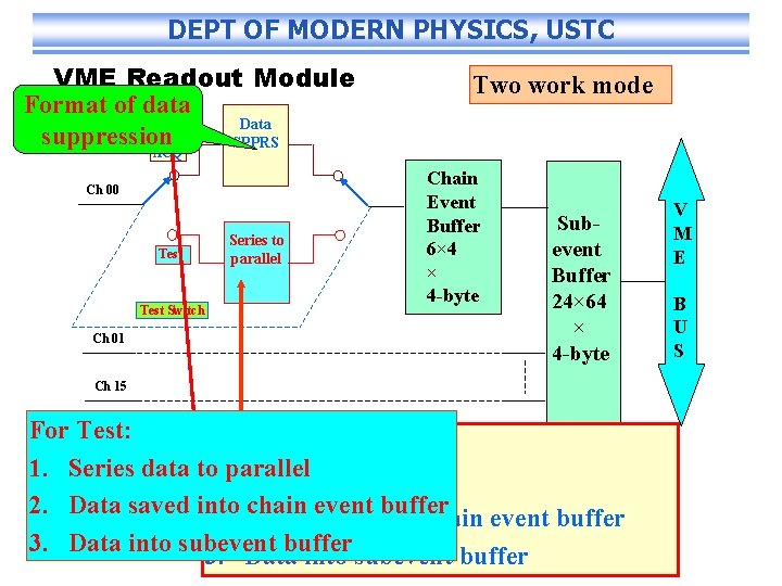
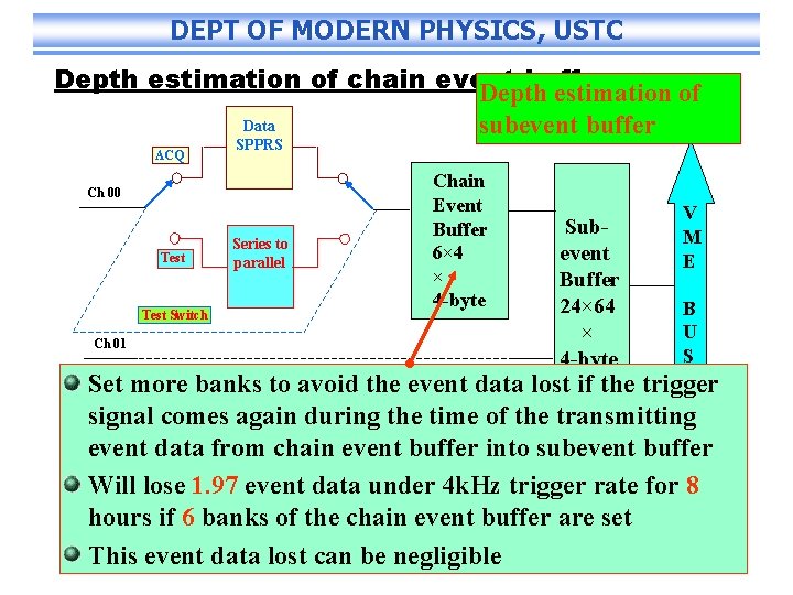
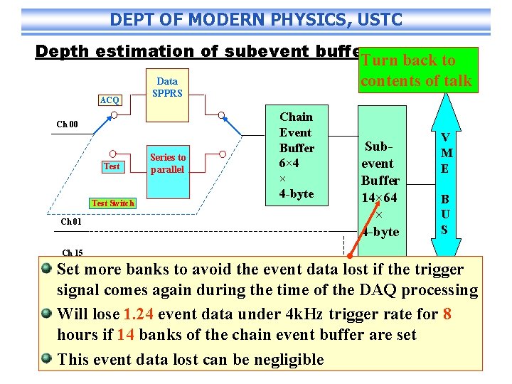
DEPT OF MODERN PHYSICS, USTC VME Readout Module Format of data Data suppression SPPRS Two work mode ACQ Ch 00 Test Switch Ch 01 Series to parallel Chain Event Buffer 6× 4 × 4 -byte Subevent Buffer 24× 64 × 4 -byte Ch 15 For Test: For data acquisition: 1. Series data to 1. parallel Data suppressions 2. Data saved into chainsaved eventinto buffer 2. Data chain event buffer 3. Data into subevent buffer V M E B U S

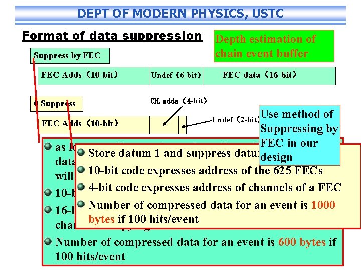
DEPT OF MODERN PHYSICS, USTC Format of data suppression Suppress by FEC Adds(10 -bit) 0 Suppress Undef(6 -bit) Depth estimation of chain event buffer FEC data(16 -bit) CH. adds(4 -bit) Use method of FEC Adds(10 -bit) Suppressing by FECappears, in our as long. Store as a datum of one channel on a FEC datum 1 and suppress datum 0 design data of whole 16 channels on a FEC as a 16 -bit word will be 10 -bit storedcode expresses address of the 625 FECs 4 -bit expresses code expresses addressofofthe channels of a FEC 10 -bit code the address 625 FECs Number of compressed an event is 1000 16 -bit code expresses the data of 16 for channels, each bytes if 100 hits/event channel occupying one bit Undef(2 -bit) Number of compressed data for an event is 600 bytes if 100 hits/event

DEPT OF MODERN PHYSICS, USTC Depth estimation of chain event buffer Depth estimation of Data subevent buffer ACQ SPPRS Ch 00 Test Switch Ch 01 Series to parallel Chain Event Buffer 6× 4 × 4 -byte Subevent Buffer 24× 64 × 4 -byte V M E B U S Set Ch 15 more banks to avoid the event data lost if the trigger signal comes again during the time of the transmitting event data from chain event buffer into subevent buffer Will lose 1. 97 event data under 4 k. Hz trigger rate for 8 hours if 6 banks of the chain event buffer are set This event data lost can be negligible

DEPT OF MODERN PHYSICS, USTC Depth estimation of subevent buffer Turn back to Data contents of talk ACQ SPPRS Ch 00 Test Switch Ch 01 Series to parallel Chain Event Buffer 6× 4 × 4 -byte Subevent Buffer 14× 64 × 4 -byte V M E B U S Ch 15 Set more banks to avoid the event data lost if the trigger signal comes again during the time of the DAQ processing Will lose 1. 24 event data under 4 k. Hz trigger rate for 8 hours if 14 banks of the chain event buffer are set This event data lost can be negligible

DEPT OF MODERN PHYSICS, USTC CONTENTS Overview of structure Readout System of MC Test System of MC

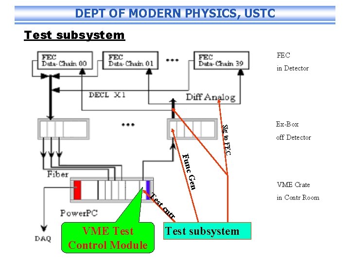
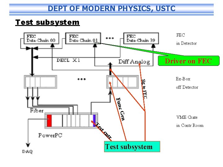
DEPT OF MODERN PHYSICS, USTC Test subsystem Sig to FEC F unc Gen Te st cn tr VME Test Control Module Test subsystem

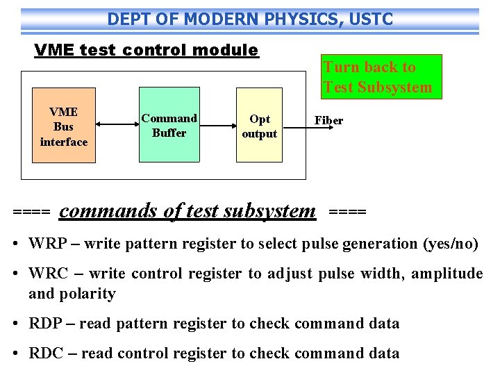
DEPT OF MODERN PHYSICS, USTC VME test control module VME Bus interface ==== Command Buffer Opt output Turn back to Test Subsystem Fiber commands of test subsystem ==== • WRP – write pattern register to select pulse generation (yes/no) • WRC – write control register to adjust pulse width, amplitude and polarity • RDP – read pattern register to check command data • RDC – read control register to check command data

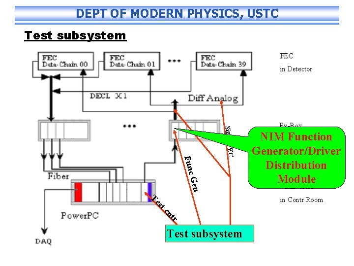
DEPT OF MODERN PHYSICS, USTC Test subsystem Sig to FEC F unc Gen Te st cn tr Test subsystem NIM Function Generator/Driver Distribution Module

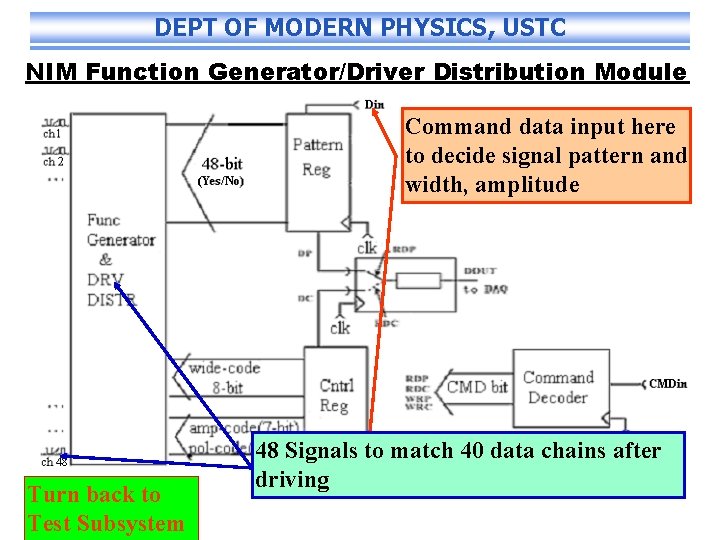
DEPT OF MODERN PHYSICS, USTC NIM Function Generator/Driver Distribution Module Command data input here to decide signal pattern and width, amplitude Turn back to Test Subsystem 48 Signals to match 40 data chains after driving

DEPT OF MODERN PHYSICS, USTC Test subsystem Driver on FEC Sig to FEC F unc Gen Te st cn tr Test subsystem

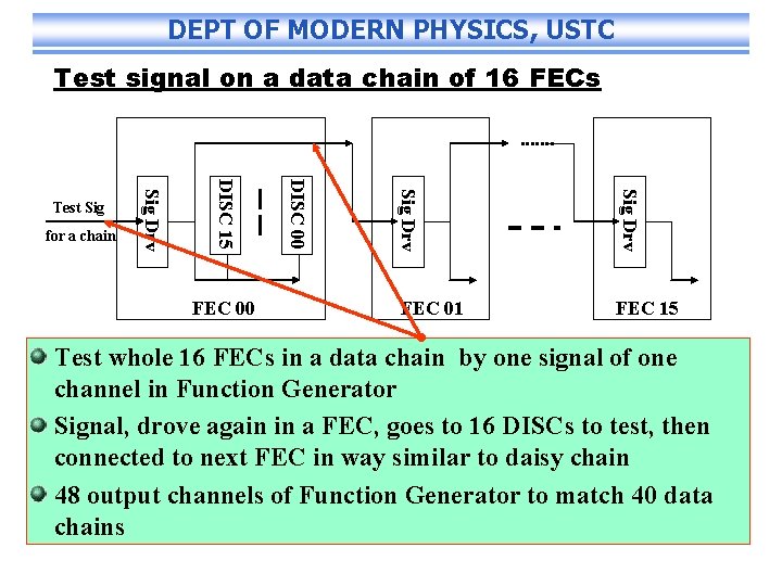
DEPT OF MODERN PHYSICS, USTC Test signal on a data chain of 16 FECs Sig Drv FEC 00 DISC 15 for a chain Sig Drv Test Sig FEC 01 FEC 15 Test whole 16 FECs in a data chain by one signal of one channel in Function Generator Signal, drove again in a FEC, goes to 16 DISCs to test, then connected to next FEC in way similar to daisy chain 48 output channels of Function Generator to match 40 data chains

DEPT OF MODERN PHYSICS, USTC Structure of MC Electronics system The End

DEPT OF MODERN PHYSICS, USTC Thanks a lot