Department of Electrical Engineering ESAT Update of the
- Slides: 21

Department of Electrical Engineering (ESAT) Update of the “Digital EMC project” February 6 th, 2007 Junfeng Zhou Promotor: Prof. Wim Dehaene KULeuven ESAT-MICAS

Outline Department of Electrical Engineering (ESAT) Part I: AMIS problems on RD 2 E PCB and Chip Part II: di/dt measurement Part III: Improved EMI-Suppressing regulator structure Part IV: Future work MICAS

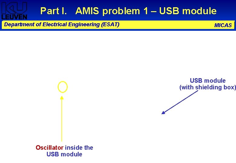
Part I. AMIS problem 1 – USB module Department of Electrical Engineering (ESAT) MICAS USB module (with shielding box) Oscillator inside the USB module

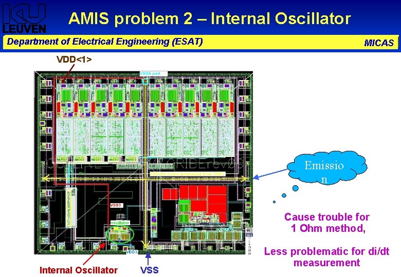
AMIS problem 2 – Internal Oscillator Department of Electrical Engineering (ESAT) MICAS VDD<1> Emissio n Cause trouble for 1 Ohm method, Internal Oscillator VSS Less problematic for di/dt measurement

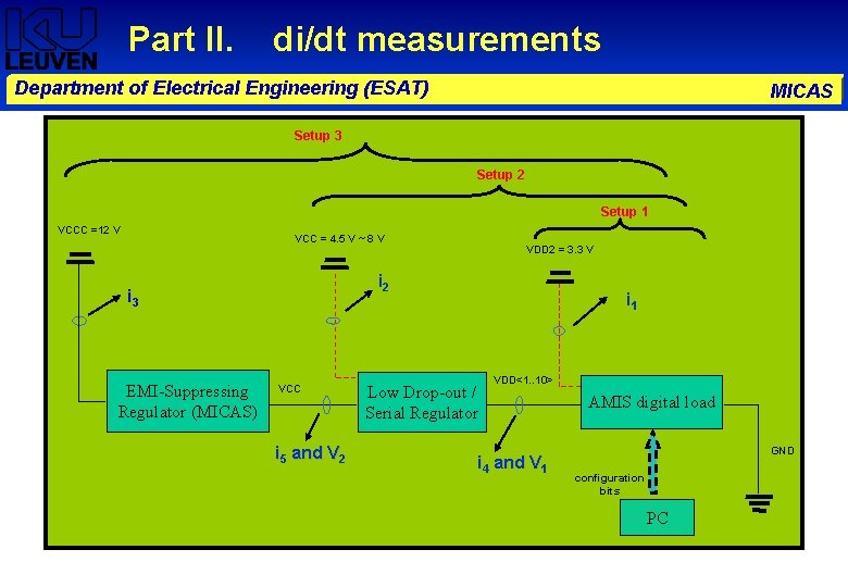
Part II. di/dt measurements Department of Electrical Engineering (ESAT) MICAS Setup 3 Setup 2 Setup 1 VCCC =12 V VCC = 4. 5 V ~ 8 V i 2 i 3 EMI-Suppressing Regulator (MICAS) VDD 2 = 3. 3 V VCC i 5 and V 2 i 1 Low Drop-out / Serial Regulator VDD<1. . 10> i 4 and V 1 AMIS digital load GND configuration bits PC

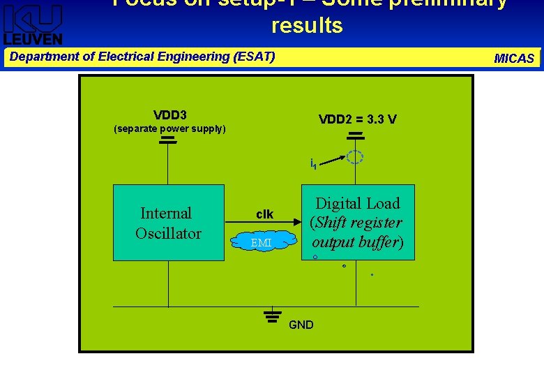
Focus on setup-1 – Some preliminary results Department of Electrical Engineering (ESAT) MICAS VDD 3 VDD 2 = 3. 3 V (separate power supply) i 1 Internal Oscillator clk EMI Digital Load (Shift register output buffer) buffer GND

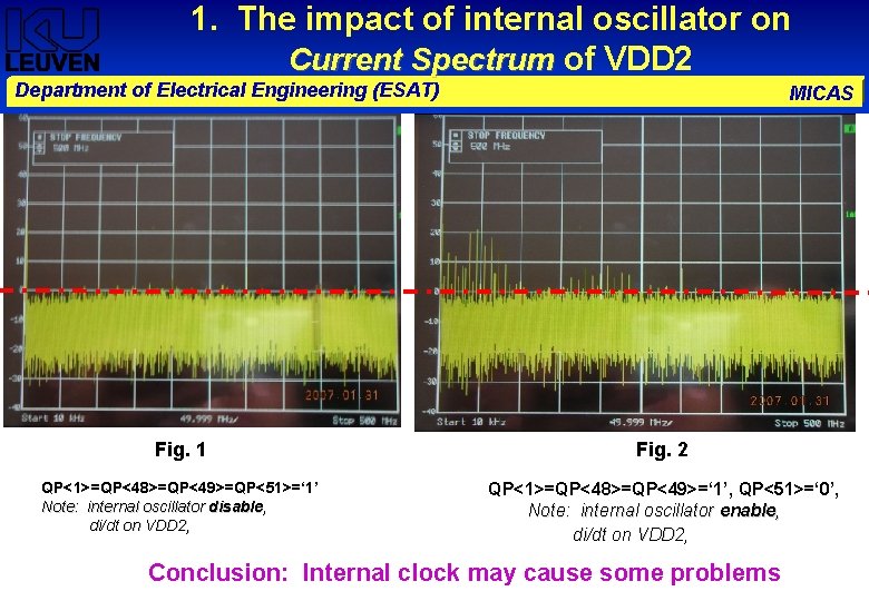
1. The impact of internal oscillator on Current Spectrum of VDD 2 Department of Electrical Engineering (ESAT) MICAS Fig. 1 Fig. 2 QP<1>=QP<48>=QP<49>=QP<51>=‘ 1’ Note: internal oscillator disable, di/dt on VDD 2, QP<1>=QP<48>=QP<49>=‘ 1’, QP<51>=‘ 0’, Note: internal oscillator enable, di/dt on VDD 2, Conclusion: Internal clock may cause some problems

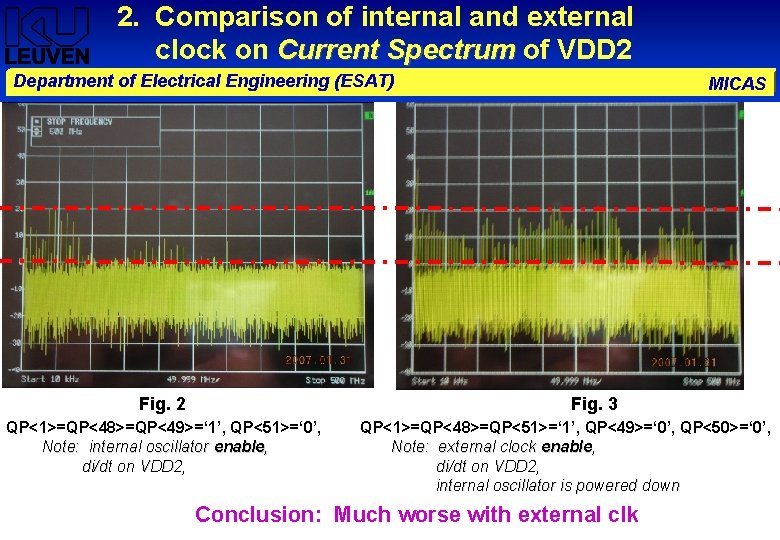
2. Comparison of internal and external clock on Current Spectrum of VDD 2 Department of Electrical Engineering (ESAT) Fig. 2 MICAS Fig. 3 QP<1>=QP<48>=QP<49>=‘ 1’, QP<51>=‘ 0’, Note: internal oscillator enable, di/dt on VDD 2, QP<1>=QP<48>=QP<51>=‘ 1’, QP<49>=‘ 0’, QP<50>=‘ 0’, Note: external clock enable, di/dt on VDD 2, internal oscillator is powered down Conclusion: Much worse with external clk

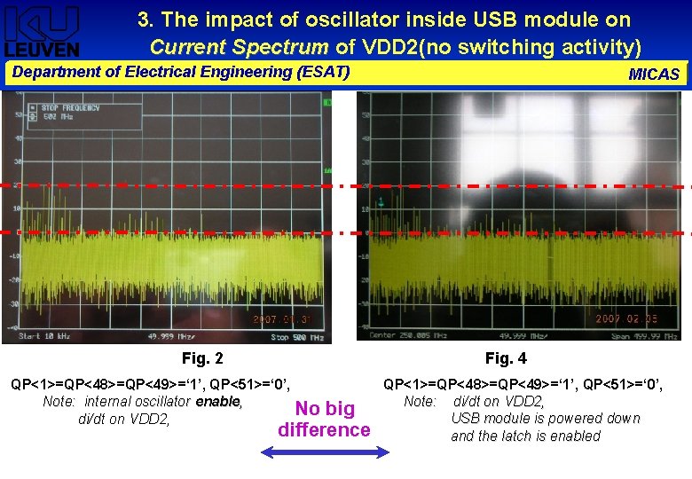
3. The impact of oscillator inside USB module on Current Spectrum of VDD 2(no switching activity) Department of Electrical Engineering (ESAT) Fig. 2 MICAS Fig. 4 QP<1>=QP<48>=QP<49>=‘ 1’, QP<51>=‘ 0’, Note: internal oscillator enable, No di/dt on VDD 2, big difference QP<1>=QP<48>=QP<49>=‘ 1’, QP<51>=‘ 0’, Note: di/dt on VDD 2, USB module is powered down and the latch is enabled

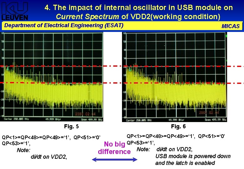
4. The impact of internal oscillator in USB module on Current Spectrum of VDD 2(working condition) Department of Electrical Engineering (ESAT) Fig. 5 Fig. 6 QP<1>=QP<48>=QP<49>=‘ 1’, QP<51>=‘ 0’ QP<53>=‘ 1’, Note: di/dt on VDD 2, MICAS QP<1>=QP<48>=QP<49>=‘ 1’, QP<51>=‘ 0’ big QP<53>=‘ 1’, No difference Note: di/dt on VDD 2, USB module is powered down and the latch is enabled

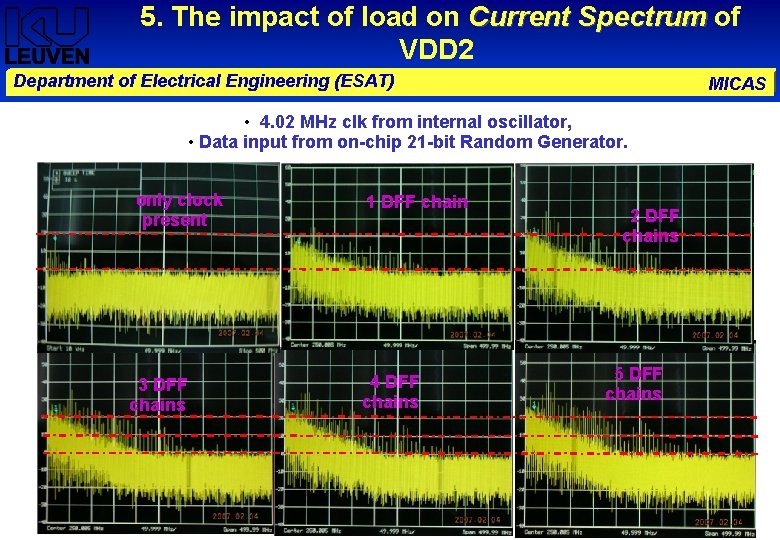
5. The impact of load on Current Spectrum of VDD 2 Department of Electrical Engineering (ESAT) MICAS • 4. 02 MHz clk from internal oscillator, • Data input from on-chip 21 -bit Random Generator. only clock present 3 DFF chains 1 DFF chain 4 DFF chains 2 DFF chains 5 DFF chains

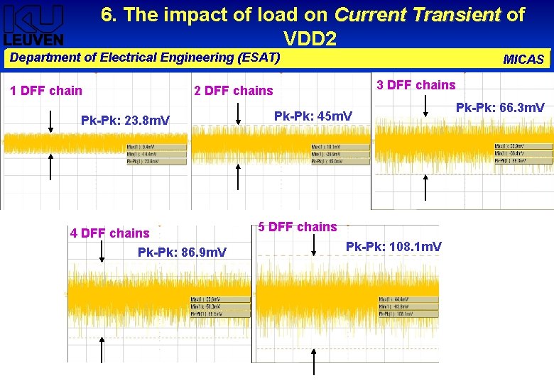
6. The impact of load on Current Transient of VDD 2 Department of Electrical Engineering (ESAT) 1 DFF chain MICAS 3 DFF chains 2 DFF chains Pk-Pk: 23. 8 m. V 4 DFF chains Pk-Pk: 86. 9 m. V Pk-Pk: 45 m. V 5 DFF chains Pk-Pk: 108. 1 m. V Pk-Pk: 66. 3 m. V

7. The impact of load on di/dt Transient of VDD 2 Department of Electrical Engineering (ESAT) MICAS In general, as more DFF chains are on, the di/dt peak increases proportionally.

Conclusions Department of Electrical Engineering (ESAT) MICAS On-chip internal oscillator won’t hurt much, which is common for all measurements. Oscillator inside USB module is not a problem at all, shielding box can do most of the job. Setup for massive measurements is in preparation Automatic setup shall be ok by this week, Agreement on data to be measured ?

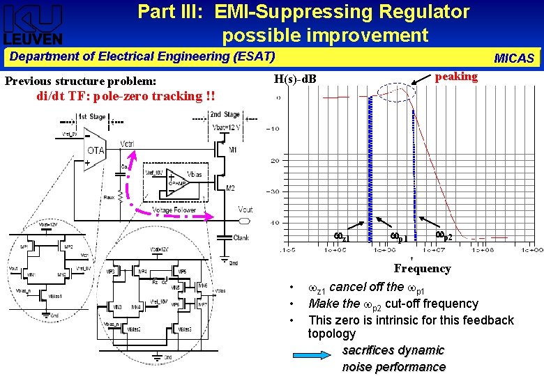
Part III: EMI-Suppressing Regulator possible improvement Department of Electrical Engineering (ESAT) Previous structure problem: MICAS peaking H(s)-d. B di/dt TF: pole-zero tracking !! z 1 p 2 Frequency • • • z 1 cancel off the p 1 Make the p 2 cut-off frequency This zero is intrinsic for this feedback topology sacrifices dynamic noise performance

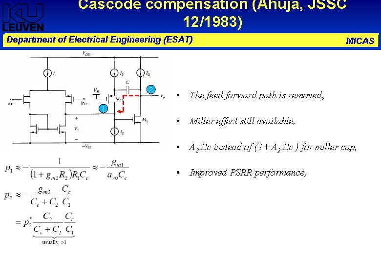
Cascode compensation (Ahuja, JSSC 12/1983) Department of Electrical Engineering (ESAT) 2 MICAS • The feed forward path is removed, 1 • Miller effect still available, • A 2 Cc instead of (1+ A 2 Cc ) for miller cap, • Improved PSRR performance,

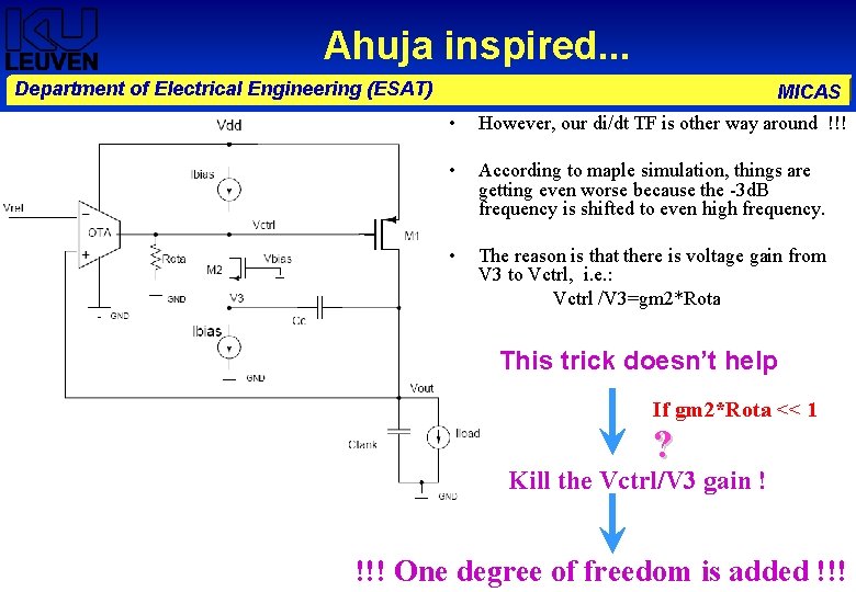
Ahuja inspired. . . Department of Electrical Engineering (ESAT) MICAS • However, our di/dt TF is other way around !!! • According to maple simulation, things are getting even worse because the -3 d. B frequency is shifted to even high frequency. • The reason is that there is voltage gain from V 3 to Vctrl, i. e. : Vctrl /V 3=gm 2*Rota This trick doesn’t help If gm 2*Rota << 1 ? Kill the Vctrl/V 3 gain ! !!! One degree of freedom is added !!!

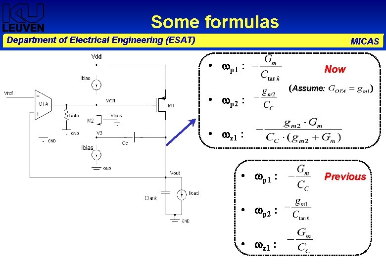
Some formulas Department of Electrical Engineering (ESAT) MICAS • p 1 : • p 2 : Now (Assume: • z 1 : • p 2 : • z 1 : Previous )

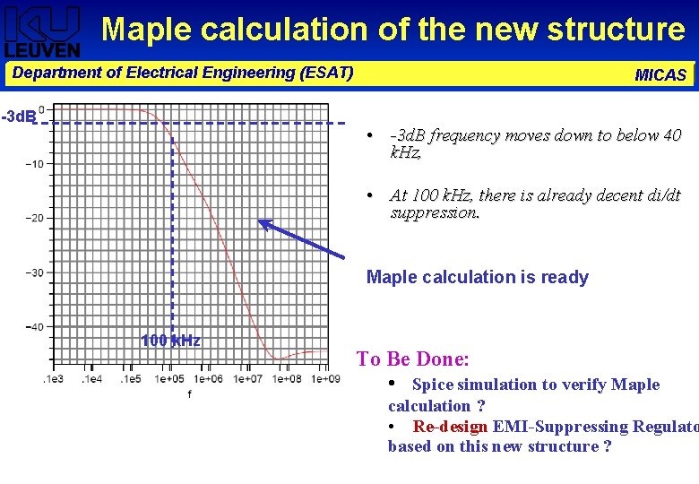
Maple calculation of the new structure Department of Electrical Engineering (ESAT) -3 d. B MICAS • -3 d. B frequency moves down to below 40 k. Hz, • At 100 k. Hz, there is already decent di/dt suppression. Maple calculation is ready 100 k. Hz To Be Done: • Spice simulation to verify Maple calculation ? • Re-design EMI-Suppressing Regulato based on this new structure ?

Part IV: Future Work Department of Electrical Engineering (ESAT) Continue the digital load measurements, More analysis for new structure: Stability and Transient, Spice simulation. MICAS

Questions Department of Electrical Engineering (ESAT) Thank you for your attention MICAS