Delta 6622 Delta 3 Delta 5 Delta N


- Slides: 32

Delta 6622 Delta 3 Delta 5 Delta. N Delta. X Electra Welcome Wave process Process related Component related Board related System related 2016 Tv. T

Process related, vs 1 Component related, vs 2 Board related, vs 3 System related, vs 4

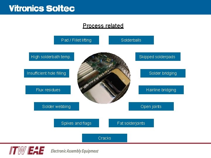
Process related Pad / Fillet lifting Solderballs High solderbath temp. Skipped solderpads Insufficient hole filling Solder bridging Flux residues Hairline bridging Solder webbing Open joints Spikes and flags Fat solderjoints Cracks

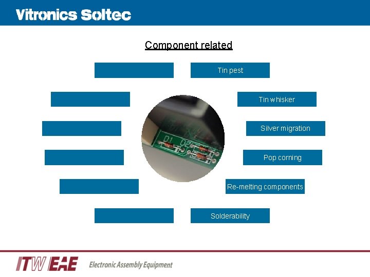
Component related Tin pest Tin whisker Silver migration Pop corning Re-melting components Solderability

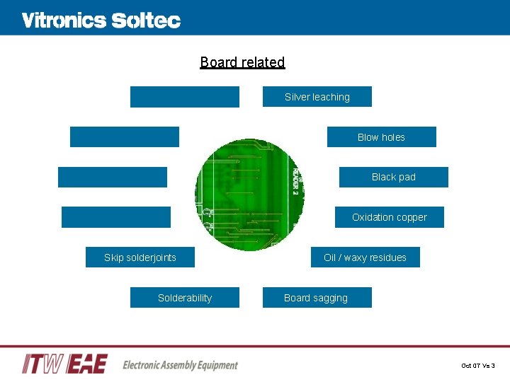
Board related Silver leaching Blow holes Black pad Oxidation copper Skip solderjoints Solderability Oil / waxy residues Board sagging Oct 07 Vs 3

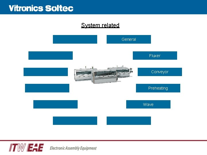
System related General Fluxer Conveyor Preheating Wave

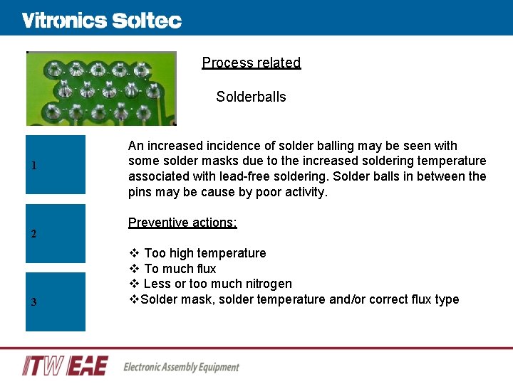
Process related Solderballs 1 2 3 An increased incidence of solder balling may be seen with some solder masks due to the increased soldering temperature associated with lead-free soldering. Solder balls in between the pins may be cause by poor activity. Preventive actions: v Too high temperature v To much flux v Less or too much nitrogen v. Solder mask, solder temperature and/or correct flux type

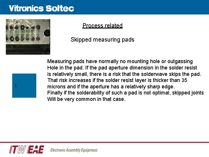
Process related Skipped measuring pads 1 Measuring pads have normally no mounting hole or outgassing Hole in the pad. If the pad aperture dimension in the solder resist is relatively small, there is a risk that the solderwave skips the pad. That risk increases if the solder resist layer is thicker than 35 microns and if the aperture has a relatively sharp edge. Finally if the solderability of such a pad is not optimal, skipped joints Will be very common in that case.

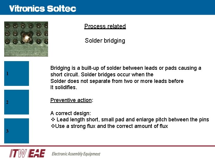
Process related Solder bridging 1 2 3 Bridging is a built-up of solder between leads or pads causing a short circuit. Solder bridges occur when the Solder does not separate from two or more leads before It solidifies. Preventive action: A correct design: v Lead length short, small pad and enlarge pitch between the pins v. Use a strong flux and the correct amount of flux

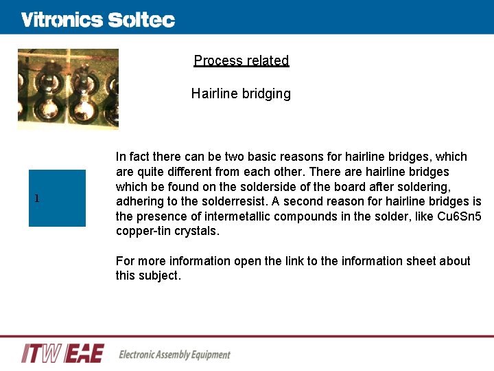
Process related Hairline bridging 1 In fact there can be two basic reasons for hairline bridges, which are quite different from each other. There are hairline bridges which be found on the solderside of the board after soldering, adhering to the solderresist. A second reason for hairline bridges is the presence of intermetallic compounds in the solder, like Cu 6 Sn 5 copper-tin crystals. For more information open the link to the information sheet about this subject.

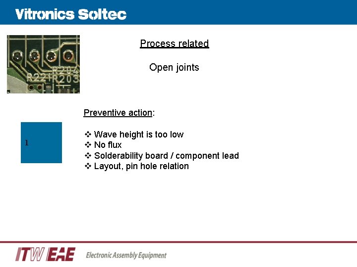
Process related Open joints Preventive action: 1 v Wave height is too low v No flux v Solderability board / component lead v Layout, pin hole relation

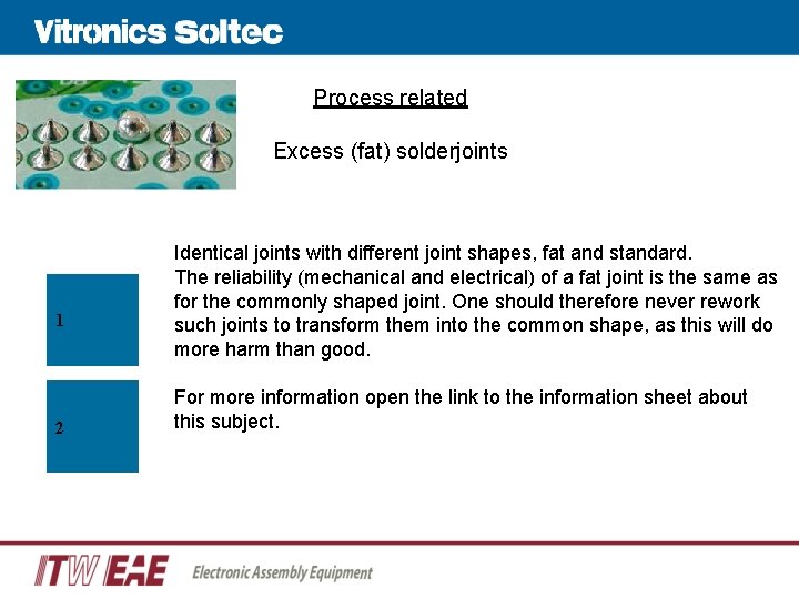
Process related Excess (fat) solderjoints 1 2 Identical joints with different joint shapes, fat and standard. The reliability (mechanical and electrical) of a fat joint is the same as for the commonly shaped joint. One should therefore never rework such joints to transform them into the common shape, as this will do more harm than good. For more information open the link to the information sheet about this subject.

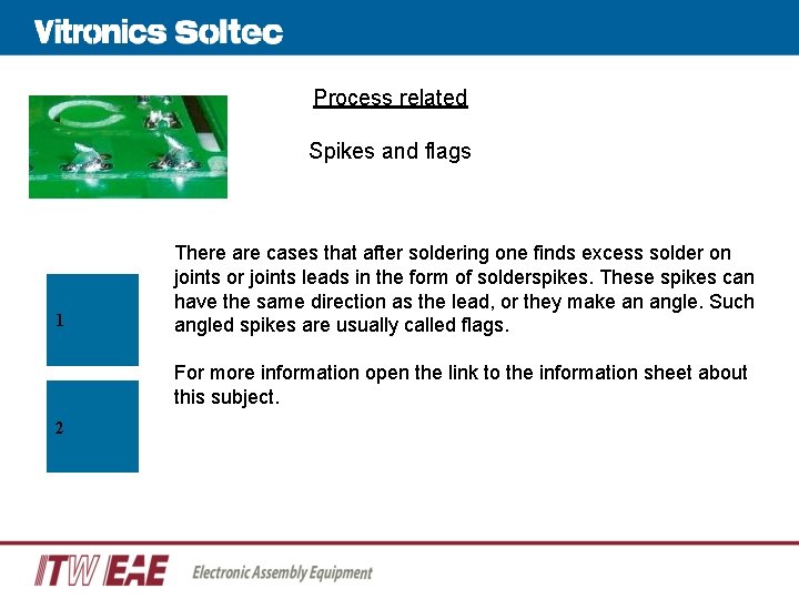
Process related Spikes and flags 1 There are cases that after soldering one finds excess solder on joints or joints leads in the form of solderspikes. These spikes can have the same direction as the lead, or they make an angle. Such angled spikes are usually called flags. For more information open the link to the information sheet about this subject. 2

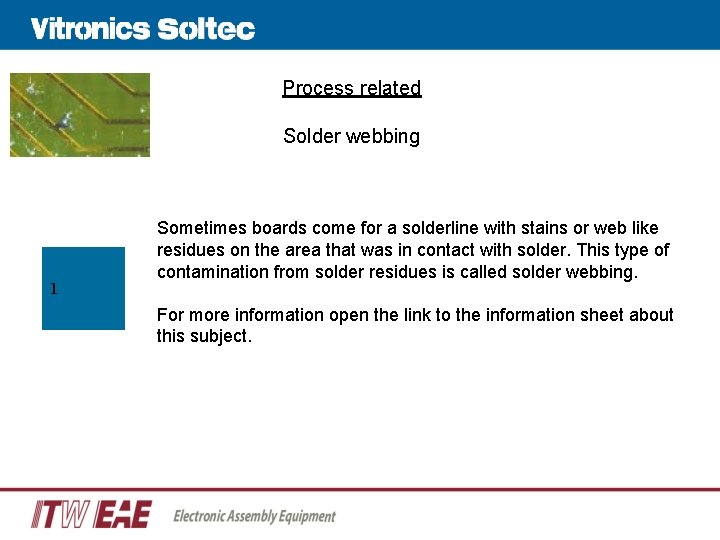
Process related Solder webbing 1 Sometimes boards come for a solderline with stains or web like residues on the area that was in contact with solder. This type of contamination from solder residues is called solder webbing. For more information open the link to the information sheet about this subject.

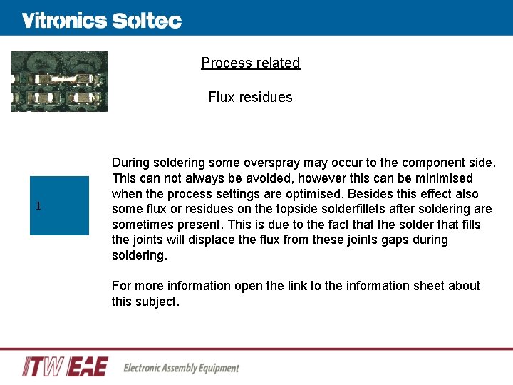
Process related Flux residues 1 During soldering some overspray may occur to the component side. This can not always be avoided, however this can be minimised when the process settings are optimised. Besides this effect also some flux or residues on the topside solderfillets after soldering are sometimes present. This is due to the fact that the solder that fills the joints will displace the flux from these joints gaps during soldering. For more information open the link to the information sheet about this subject.

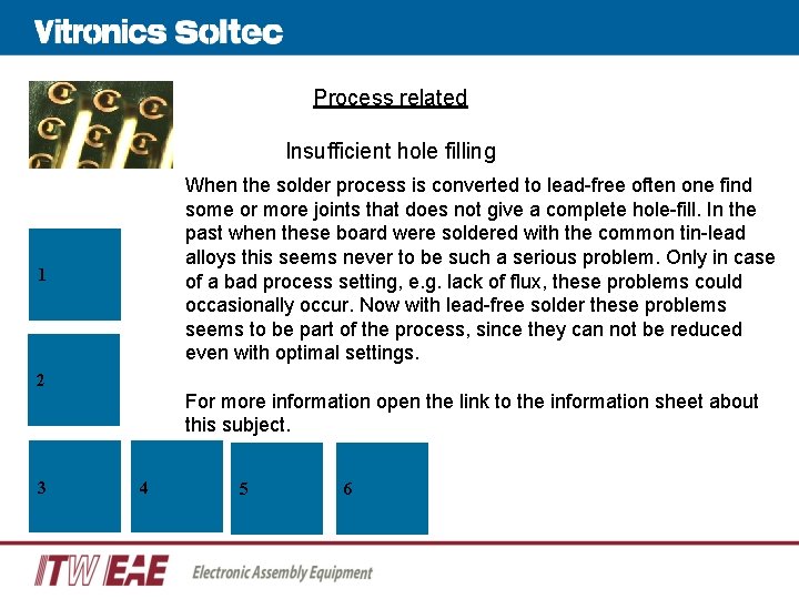
Process related Insufficient hole filling When the solder process is converted to lead-free often one find some or more joints that does not give a complete hole-fill. In the past when these board were soldered with the common tin-lead alloys this seems never to be such a serious problem. Only in case of a bad process setting, e. g. lack of flux, these problems could occasionally occur. Now with lead-free solder these problems seems to be part of the process, since they can not be reduced even with optimal settings. 1 2 3 For more information open the link to the information sheet about this subject. 4 5 6

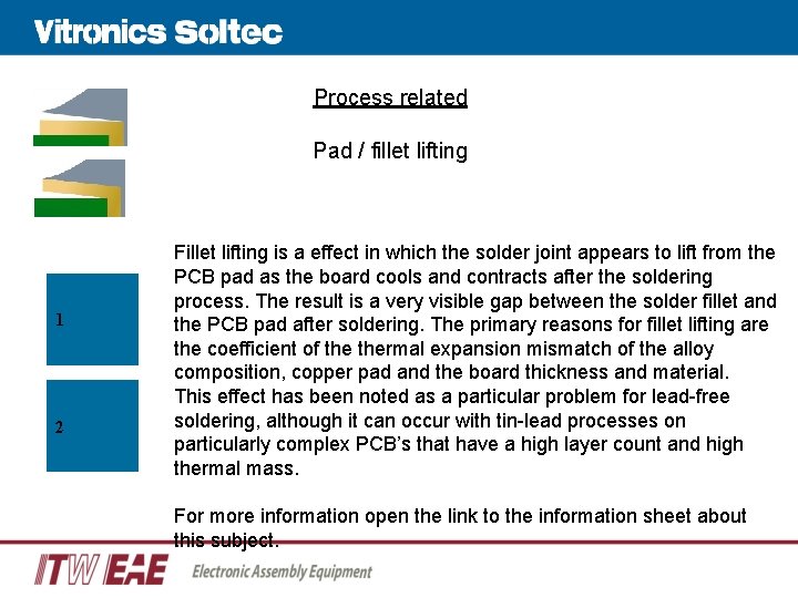
Process related Pad / fillet lifting 1 2 Fillet lifting is a effect in which the solder joint appears to lift from the PCB pad as the board cools and contracts after the soldering process. The result is a very visible gap between the solder fillet and the PCB pad after soldering. The primary reasons for fillet lifting are the coefficient of thermal expansion mismatch of the alloy composition, copper pad and the board thickness and material. This effect has been noted as a particular problem for lead-free soldering, although it can occur with tin-lead processes on particularly complex PCB’s that have a high layer count and high thermal mass. For more information open the link to the information sheet about this subject.

Process related Cracks During solidification of a solderjoint part of the solder on the coldest part of the 1 topside fillet will already be solidified, while the bulk of the solder in the joint will shrink by about 4%. 2 As a result of that this already solidified upper part will rupture from the remaining fillet.

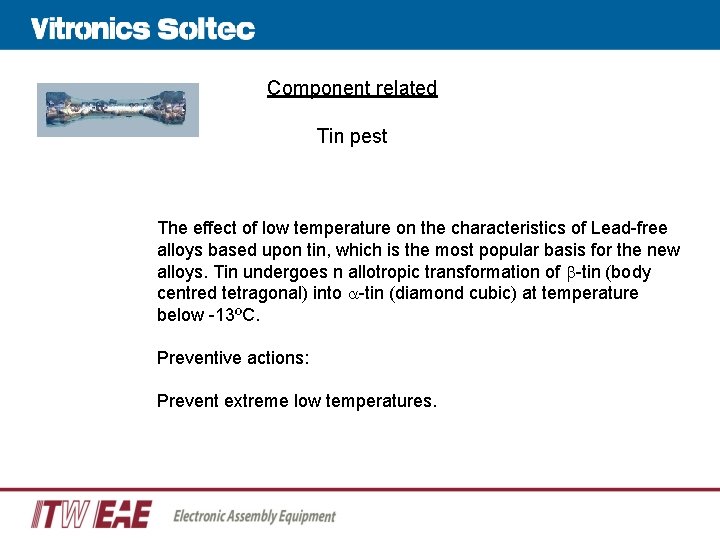
Component related Tin pest The effect of low temperature on the characteristics of Lead-free alloys based upon tin, which is the most popular basis for the new alloys. Tin undergoes n allotropic transformation of -tin (body centred tetragonal) into -tin (diamond cubic) at temperature below -13ºC. Preventive actions: Prevent extreme low temperatures.

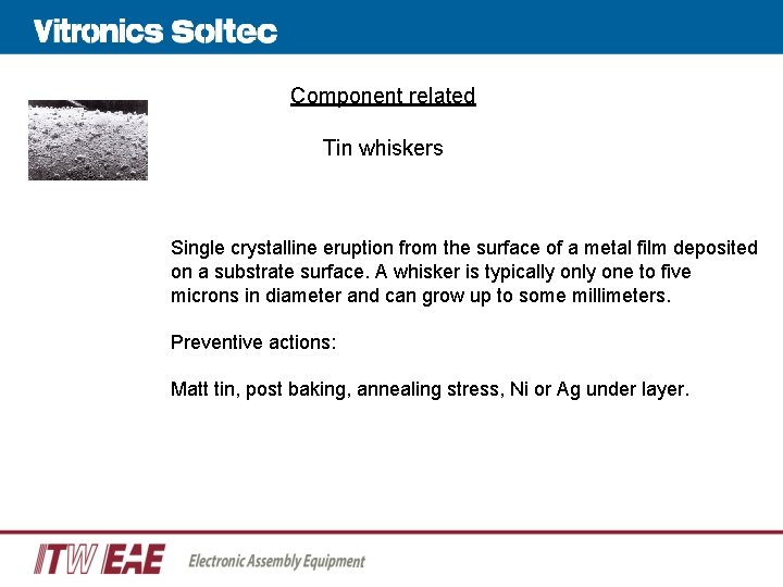
Component related Tin whiskers Single crystalline eruption from the surface of a metal film deposited on a substrate surface. A whisker is typically one to five microns in diameter and can grow up to some millimeters. Preventive actions: Matt tin, post baking, annealing stress, Ni or Ag under layer.

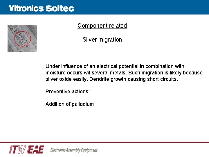
Component related Silver migration Under influence of an electrical potential in combination with moisture occurs wit several metals. Such migration is likely because silver oxide easily. Dendrite growth causing short circuits. Preventive actions: Addition of palladium.

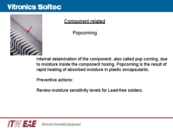
Component related Popcorning Internal delamination of the component, also called pop corning, due to moisture inside the component hosing. Popcorning is the result of rapid heating of absorbed moisture in plastic encapsulants. Preventive actions: Review moisture sensitivity levels for Lead-free solders.

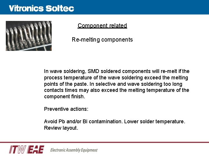
Component related Re-melting components In wave soldering, SMD soldered components will re-melt if the process temperature of the wave soldering exceed the melting points of the paste. In selective and wave soldering too long contacts times may also exceed the melting temperature of the component finish. Preventive actions: Avoid Pb and/or Bi contamination. Lower solder temperature. Review layout.

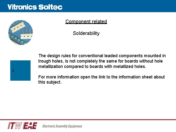
Component related Solderability 1 The design rules for conventional leaded components mounted in trough holes, is not completely the same for boards without hole metallization compared to boards with metallized holes. For more information open the link to the information sheet about this subject.

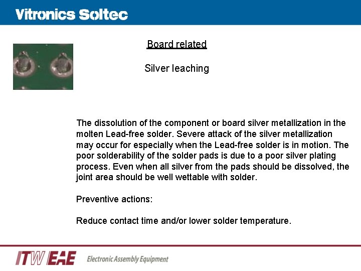
Board related Silver leaching The dissolution of the component or board silver metallization in the molten Lead-free solder. Severe attack of the silver metallization may occur for especially when the Lead-free solder is in motion. The poor solderability of the solder pads is due to a poor silver plating process. Even when all silver from the pads should be dissolved, the joint area should be well wettable with solder. Preventive actions: Reduce contact time and/or lower solder temperature.

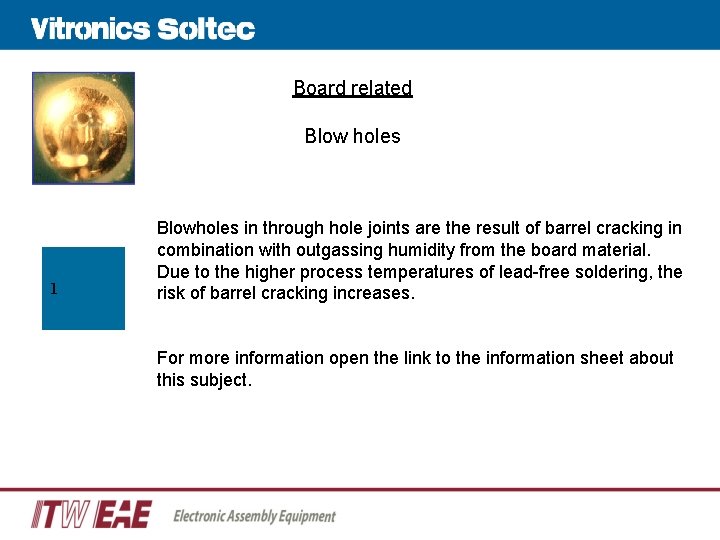
Board related Blow holes 1 Blowholes in through hole joints are the result of barrel cracking in combination with outgassing humidity from the board material. Due to the higher process temperatures of lead-free soldering, the risk of barrel cracking increases. For more information open the link to the information sheet about this subject.

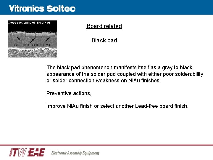
Board related Black pad The black pad phenomenon manifests itself as a gray to black appearance of the solder pad coupled with either poor solderability or solder connection weakness on Ni. Au finishes. Preventive actions, Improve Ni. Au finish or select another Lead-free board finish.

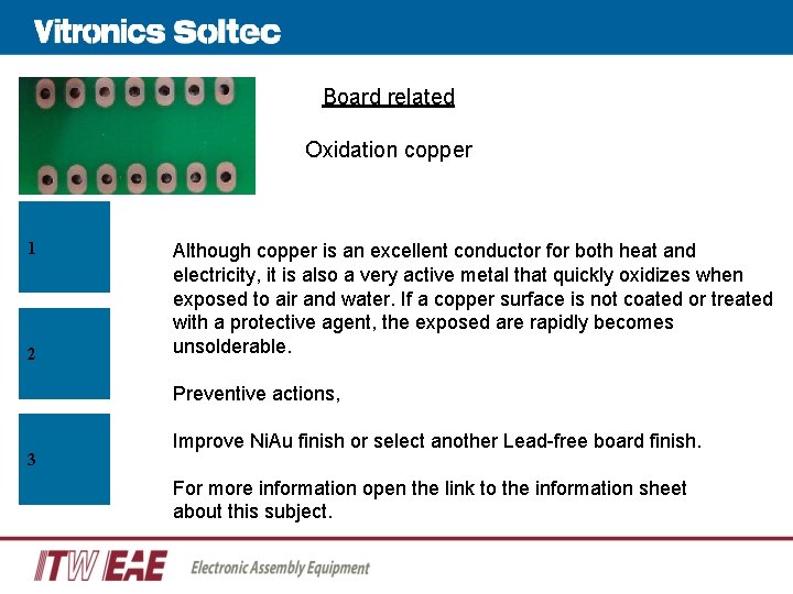
Board related Oxidation copper 1 2 Although copper is an excellent conductor for both heat and electricity, it is also a very active metal that quickly oxidizes when exposed to air and water. If a copper surface is not coated or treated with a protective agent, the exposed are rapidly becomes unsolderable. Preventive actions, 3 Improve Ni. Au finish or select another Lead-free board finish. For more information open the link to the information sheet about this subject.

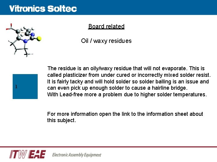
Board related Oil / waxy residues 1 The residue is an oily/waxy residue that will not evaporate. This is called plasticizer from under cured or incorrectly mixed solder resist. It is fairly tacky and will hold solder so solder balling is an issue and can even pick up enough solder to cause a hairline bridge. With Lead-free more a problem due to higher solder temperatures. For more information open the link to the information sheet about this subject.

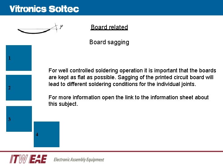
Board related Board sagging 1 For well controlled soldering operation it is important that the boards are kept as flat as possible. Sagging of the printed circuit board will lead to different soldering conditions for the individual joints. 2 For more information open the link to the information sheet about this subject. 3 4

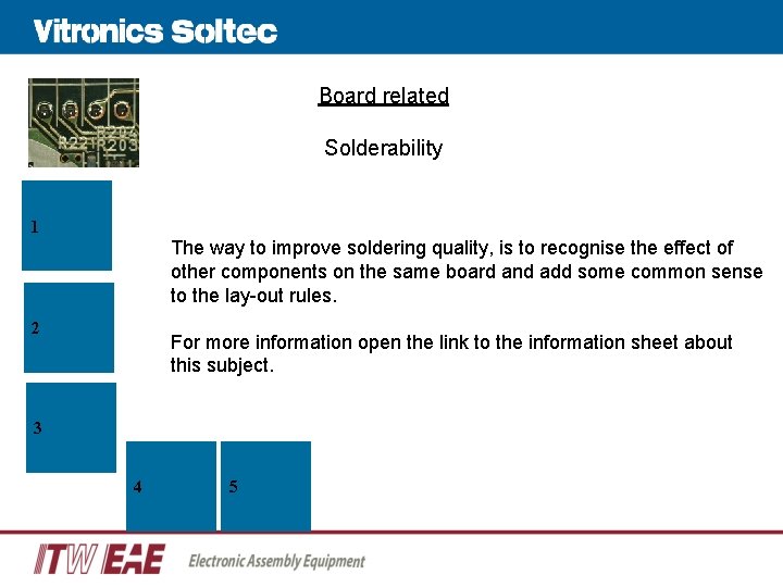
Board related Solderability 1 The way to improve soldering quality, is to recognise the effect of other components on the same board and add some common sense to the lay-out rules. 2 For more information open the link to the information sheet about this subject. 3 4 5

Thanks for your attention Your trust in us And our future cooperation For Application or general questions, please contact: