Defecttolerant FPGA Switch Block and Connection Block with
Defect-tolerant FPGA Switch Block and Connection Block with Fine-grain Redundancy for Yield Enhancement Anthony J. Yu Guy G. F. Lemieux August 25, 2005 FPL'05 - Presentation
Outline Introduction and Motivation Previous Approaches Fine-grain Redundancy Results Conclusions FPL'05 - Presentation 2
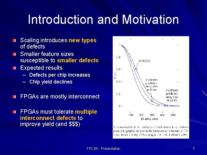
Introduction and Motivation Scaling introduces new types of defects Smaller feature sizes susceptible to smaller defects Expected results – Defects per chip increases – Chip yield declines FPGAs are mostly interconnect FPGAs must tolerate multiple interconnect defects to improve yield (and $$$) FPL'05 - Presentation 3
General Defect Tolerant Techniques Defect-tolerant techniques minimize impact (cost) of manufacturing defects FPGA defect-tolerance can be loosely categorized into three classes: – Software Redundancy – use CAD tools to map around the defects – Hardware Redundancy – incorporate spare resources to assist in defect correction (eg. Spare row/column) – Run-time Redundancy – protection against transient faults such as SEUs (eg. TMR) FPL'05 - Presentation 4
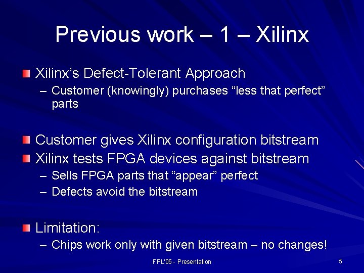
Previous work – 1 – Xilinx’s Defect-Tolerant Approach – Customer (knowingly) purchases “less that perfect” parts Customer gives Xilinx configuration bitstream Xilinx tests FPGA devices against bitstream – Sells FPGA parts that “appear” perfect – Defects avoid the bitstream Limitation: – Chips work only with given bitstream – no changes! FPL'05 - Presentation 5
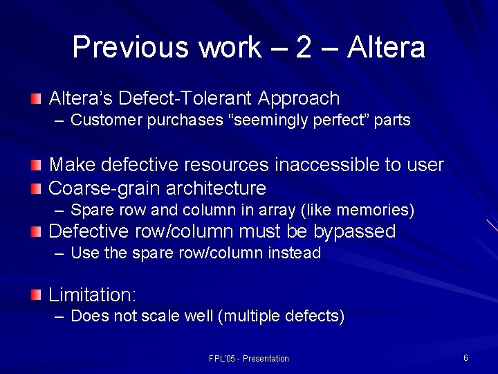
Previous work – 2 – Altera’s Defect-Tolerant Approach – Customer purchases “seemingly perfect” parts Make defective resources inaccessible to user Coarse-grain architecture – Spare row and column in array (like memories) Defective row/column must be bypassed – Use the spare row/column instead Limitation: – Does not scale well (multiple defects) FPL'05 - Presentation 6
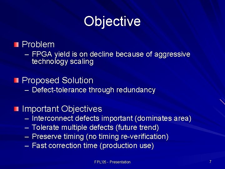
Objective Problem – FPGA yield is on decline because of aggressive technology scaling Proposed Solution – Defect-tolerance through redundancy Important Objectives – – Interconnect defects important (dominates area) Tolerate multiple defects (future trend) Preserve timing (no timing re-verification) Fast correction time (production use) FPL'05 - Presentation 7
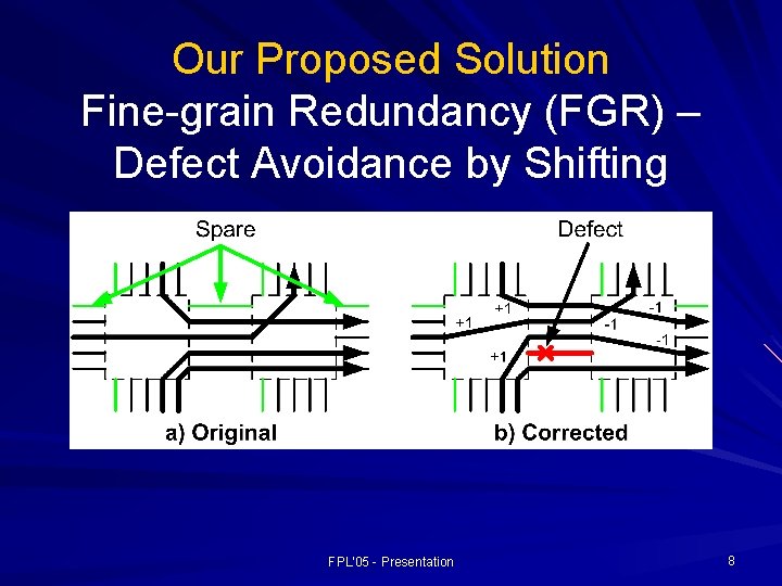
Our Proposed Solution Fine-grain Redundancy (FGR) – Defect Avoidance by Shifting FPL'05 - Presentation 8
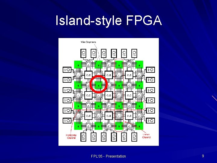
Island-style FPGA FPL'05 - Presentation 9
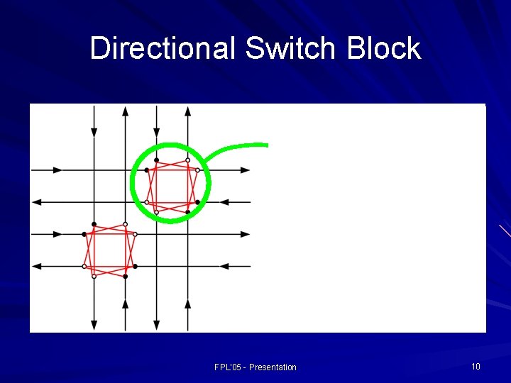
Directional Switch Block FPL'05 - Presentation 10
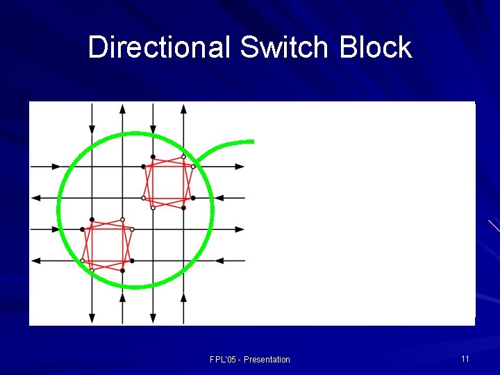
Directional Switch Block FPL'05 - Presentation 11

Defect-tolerant Switch Block FPL'05 - Presentation 12
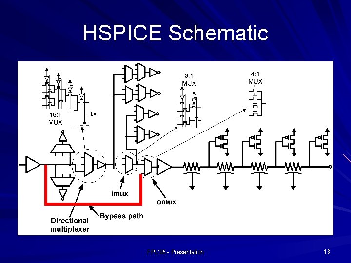
HSPICE Schematic FPL'05 - Presentation 13
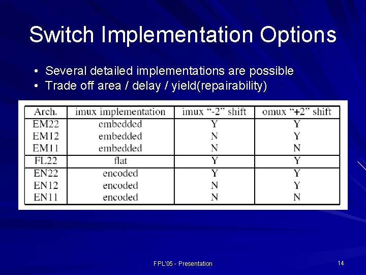
Switch Implementation Options • Several detailed implementations are possible • Trade off area / delay / yield(repairability) FPL'05 - Presentation 14
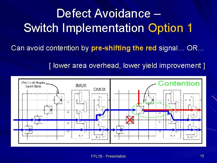
Defect Avoidance – Switch Implementation Option 1 Can avoid contention by pre-shifting the red signal… OR… [ lower area overhead, lower yield improvement ] FPL'05 - Presentation 15
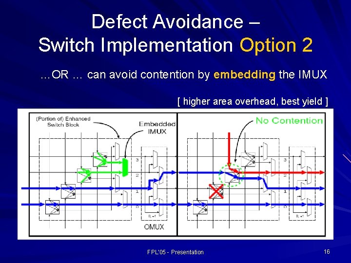
Defect Avoidance – Switch Implementation Option 2 …OR … can avoid contention by embedding the IMUX [ higher area overhead, best yield ] FPL'05 - Presentation 16
Results Area Delay Product Yield Summary FPL'05 - Presentation 17
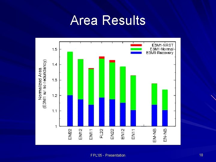
Area Results FPL'05 - Presentation 18
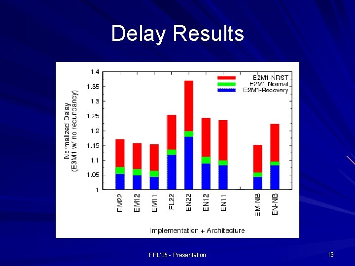
Delay Results FPL'05 - Presentation 19
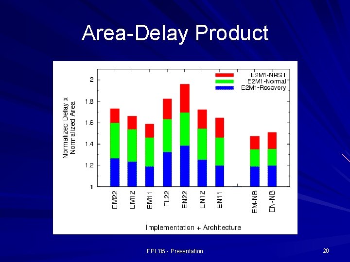
Area-Delay Product FPL'05 - Presentation 20
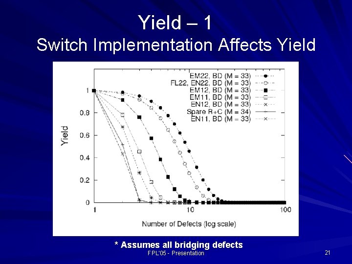
Yield – 1 Switch Implementation Affects Yield * Assumes all bridging defects FPL'05 - Presentation 21
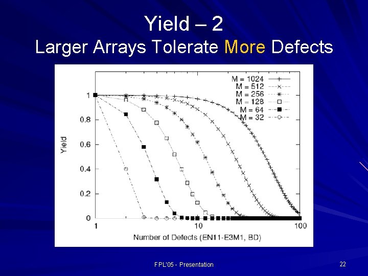
Yield – 2 Larger Arrays Tolerate More Defects FPL'05 - Presentation 22
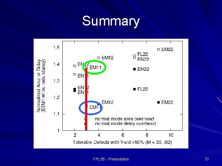
Summary FPL'05 - Presentation 23
Conclusions FGR meets desired objectives – Tolerates multiple randomly distributed defects – Defect correction does not perturb timing – Tolerates an increasing number of defects as array size increases – Correction can be applied quickly FGR has different implementation options – – Trade-offs between yield, area and delay can be made Best Area: EN 11 Best Delay: EM 11 Best Yield: EM 22 FPL'05 - Presentation 24

Thank you! anthonyy@ece. ubc. ca FPL'05 - Presentation
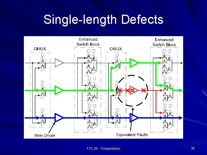
Single-length Defects FPL'05 - Presentation 26
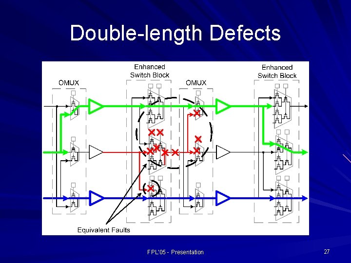
Double-length Defects FPL'05 - Presentation 27
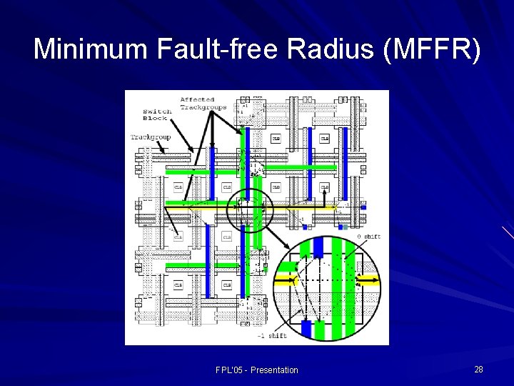
Minimum Fault-free Radius (MFFR) FPL'05 - Presentation 28
- Slides: 28