Defects Types of defects Point defects line defects

- Slides: 20

Defects • Types of defects – Point defects, line defects, planar defects and volume defects • Concentration of various defects • Movement of defects • Identification of defects • Effect of defects on electronic properties • Defect “gettering” 1 ECSE-4250 Integrated Circuit Processes & Design

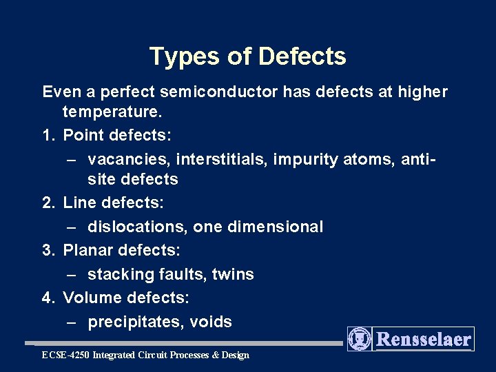
Types of Defects Even a perfect semiconductor has defects at higher temperature. 1. Point defects: – vacancies, interstitials, impurity atoms, antisite defects 2. Line defects: – dislocations, one dimensional 3. Planar defects: – stacking faults, twins 4. Volume defects: – precipitates, voids 1 ECSE-4250 Integrated Circuit Processes & Design

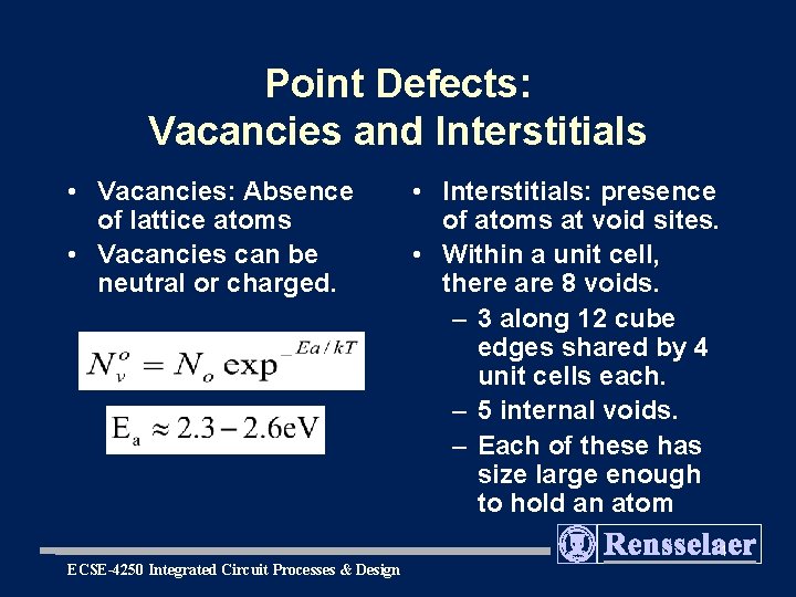
Point Defects: Vacancies and Interstitials • Vacancies: Absence of lattice atoms • Vacancies can be neutral or charged. • Interstitials: presence of atoms at void sites. • Within a unit cell, there are 8 voids. – 3 along 12 cube edges shared by 4 unit cells each. – 5 internal voids. – Each of these has size large enough to hold an atom 1 ECSE-4250 Integrated Circuit Processes & Design

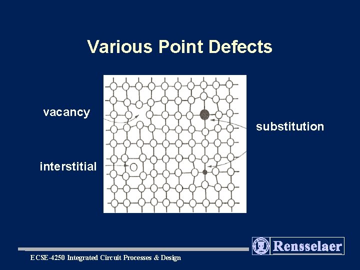
Various Point Defects vacancy substitution interstitial 1 ECSE-4250 Integrated Circuit Processes & Design

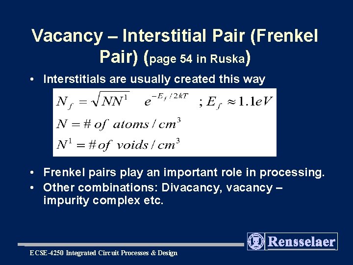
Vacancy – Interstitial Pair (Frenkel Pair) (page 54 in Ruska) • Interstitials are usually created this way • Frenkel pairs play an important role in processing. • Other combinations: Divacancy, vacancy – impurity complex etc. 1 ECSE-4250 Integrated Circuit Processes & Design

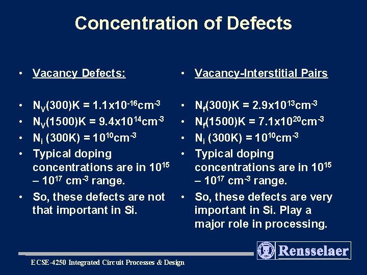
Concentration of Defects • Vacancy Defects: • Vacancy-Interstitial Pairs • • NV(300)K = 1. 1 x 10 -16 cm-3 NV(1500)K = 9. 4 x 1014 cm-3 Ni (300 K) = 1010 cm-3 Typical doping concentrations are in 1015 – 1017 cm-3 range. • So, these defects are not that important in Si. Nf(300)K = 2. 9 x 1013 cm-3 Nf(1500)K = 7. 1 x 1020 cm-3 Ni (300 K) = 1010 cm-3 Typical doping concentrations are in 1015 – 1017 cm-3 range. • So, these defects are very important in Si. Play a major role in processing. 1 ECSE-4250 Integrated Circuit Processes & Design

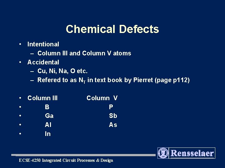
Chemical Defects • Intentional – Column III and Column V atoms • Accidental – Cu, Ni, Na, O etc. – Refered to as NT in text book by Pierret (page p 112) • Column III • B • Ga • Al • In Column V P Sb As 1 ECSE-4250 Integrated Circuit Processes & Design

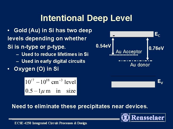
Intentional Deep Level • Gold (Au) in Si has two deep levels depending on whether 0. 54 e. V Si is n-type or p-type. – Used to reduce lifetimes in Si – Used in early digital circuits • Oxygen (O) in Si EC Au Acceptor 0. 76 e. V Au donor EV Need to eliminate these precipitates near devices. 1 ECSE-4250 Integrated Circuit Processes & Design

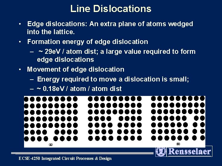
Line Dislocations • Edge dislocations: An extra plane of atoms wedged into the lattice. • Formation energy of edge dislocation – ~ 29 e. V / atom dist; a large value required to form edge dislocations • Movement of edge dislocation – Energy required to move a dislocation is small; – ~ 0. 18 e. V / atom dist 1 ECSE-4250 Integrated Circuit Processes & Design

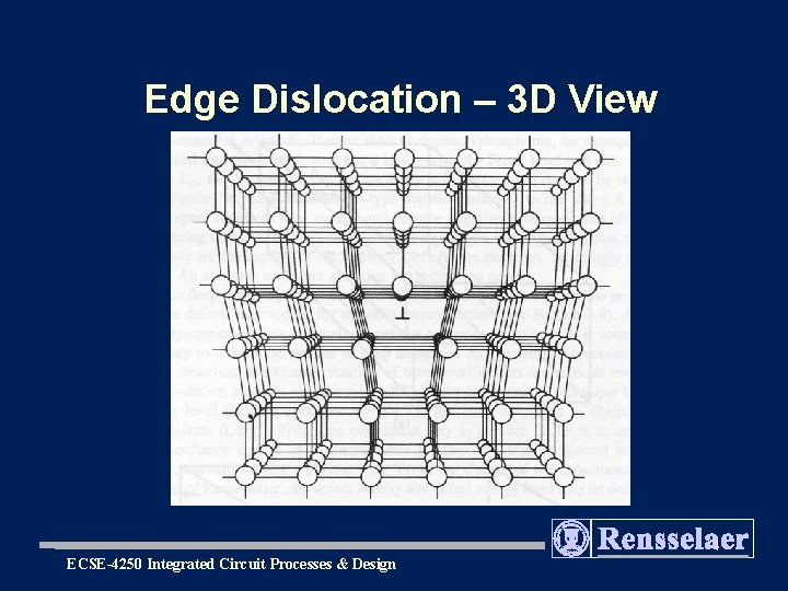
Edge Dislocation – 3 D View 1 ECSE-4250 Integrated Circuit Processes & Design

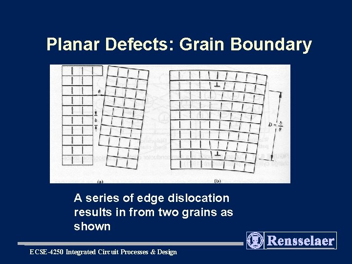
Planar Defects: Grain Boundary A series of edge dislocation results in from two grains as shown 1 ECSE-4250 Integrated Circuit Processes & Design

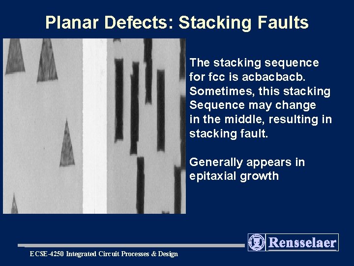
Planar Defects: Stacking Faults The stacking sequence for fcc is acbacbacb. Sometimes, this stacking Sequence may change in the middle, resulting in stacking fault. Generally appears in epitaxial growth 1 ECSE-4250 Integrated Circuit Processes & Design

What Are the Consequences? • Difficult to form dislocations thermally. Primary cause of generation is mechanical stress – Handling – Oxidation stress – Mechanical holders during processing • Once formed, easy to move. – Both good and bad! • Good: Used in “gettering” • Bad: Device leakage if present • Other major defects – Twinning, grain boundaries, stacking faults. 1 ECSE-4250 Integrated Circuit Processes & Design

Identification of Defects • Major volume defects by visual inspection • Some defects can be visually observed by “etchpits”. Also, decoration technique can be used to visually observe defects. • X-ray diffraction: defects generally broadens xray diffraction peaks • IR absorption: wafer vendors provide IR microscope pictures along with wafers. Reveals precipitates • Transmission electron microscope (TEM) 1 ECSE-4250 Integrated Circuit Processes & Design

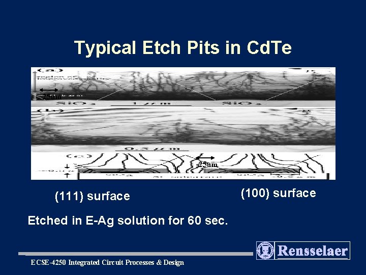
Typical Etch Pits in Cd. Te 25 um (111) surface (100) surface Etched in E-Ag solution for 60 sec. 1 ECSE-4250 Integrated Circuit Processes & Design

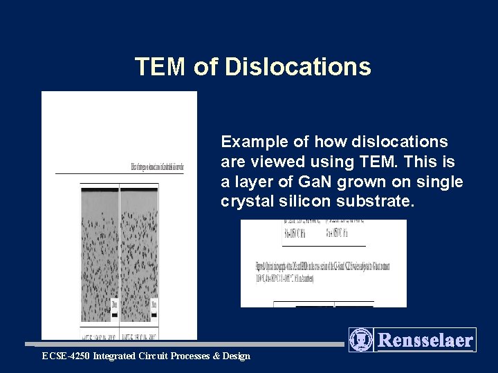
TEM of Dislocations Example of how dislocations are viewed using TEM. This is a layer of Ga. N grown on single crystal silicon substrate. 1 ECSE-4250 Integrated Circuit Processes & Design

Defect Gettering • Extrinsic gettering – Gettering of fast moving impurities by using defects as sinks – Example: damage back side of wafer and heattreat wafer at high temperature – Why do impurities decorate defects? 1 ECSE-4250 Integrated Circuit Processes & Design

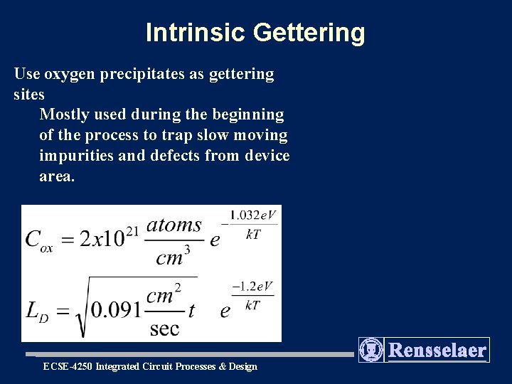
Intrinsic Gettering Use oxygen precipitates as gettering sites Mostly used during the beginning of the process to trap slow moving impurities and defects from device area. 1 ECSE-4250 Integrated Circuit Processes & Design

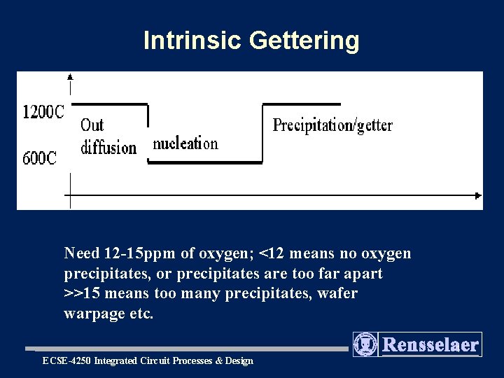
Intrinsic Gettering Need 12 -15 ppm of oxygen; <12 means no oxygen precipitates, or precipitates are too far apart >>15 means too many precipitates, wafer warpage etc. 1 ECSE-4250 Integrated Circuit Processes & Design

Semicond. Sci. Technol. 19 (2004) 548– 551 1 ECSE-4250 Integrated Circuit Processes & Design