Defects and impurities in crystalline silicon solar cells
- Slides: 28

Defects and impurities in crystalline silicon solar cells D Macdonald, F Rougieux, AY Liu, SY Lim, SP Phang, H Nguyen, Chang Sun and H Sio Research School of Engineering The Australian National University, Canberra

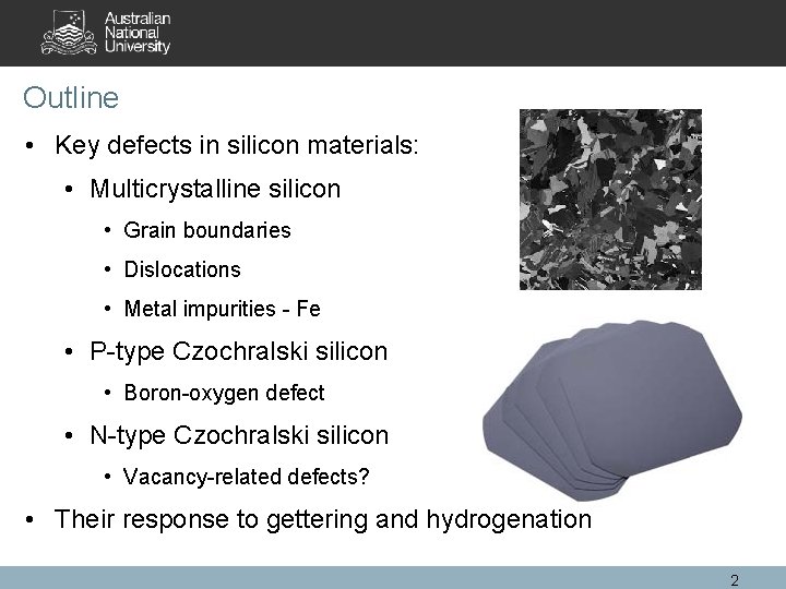
Outline • Key defects in silicon materials: • Multicrystalline silicon • Grain boundaries • Dislocations • Metal impurities - Fe • P-type Czochralski silicon • Boron-oxygen defect • N-type Czochralski silicon • Vacancy-related defects? • Their response to gettering and hydrogenation 2

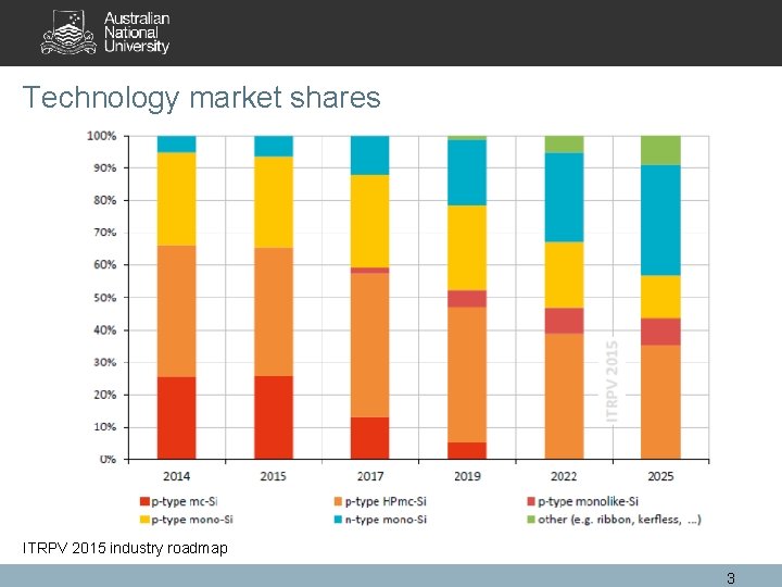
Technology market shares ITRPV 2015 industry roadmap 3

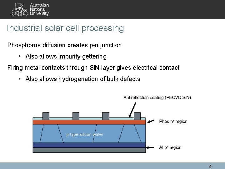
Industrial solar cell processing Phosphorus diffusion creates p-n junction • Also allows impurity gettering Firing metal contacts through Si. N layer gives electrical contact • Also allows hydrogenation of bulk defects 4

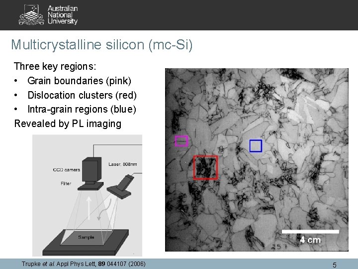
Multicrystalline silicon (mc-Si) Three key regions: • Grain boundaries (pink) • Dislocation clusters (red) • Intra-grain regions (blue) Revealed by PL imaging Trupke et al. Appl Phys Lett, 89 044107 (2006) 5

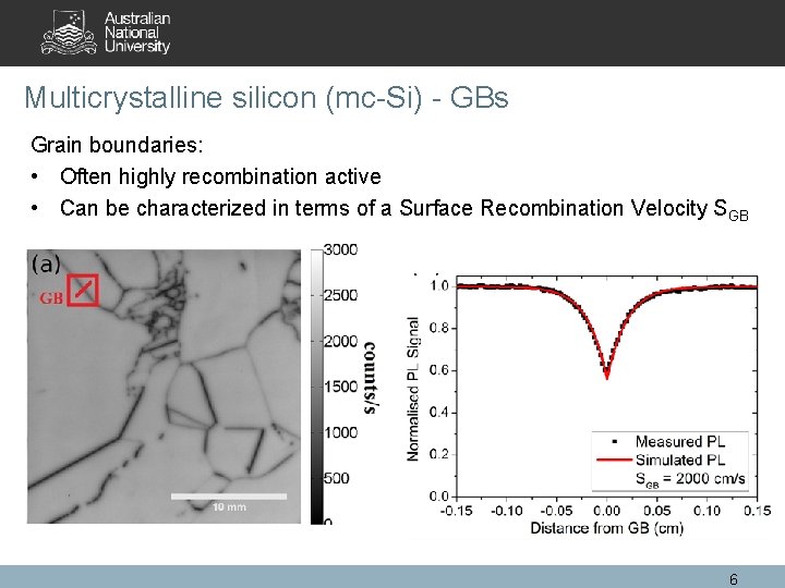
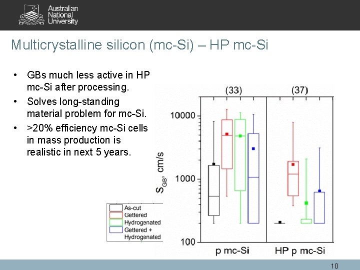
Multicrystalline silicon (mc-Si) - GBs Grain boundaries: • Often highly recombination active • Can be characterized in terms of a Surface Recombination Velocity SGB 6

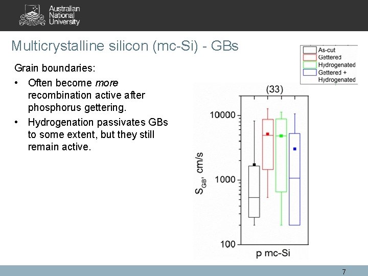
Multicrystalline silicon (mc-Si) - GBs Grain boundaries: • Often become more recombination active after phosphorus gettering. • Hydrogenation passivates GBs to some extent, but they still remain active. 7

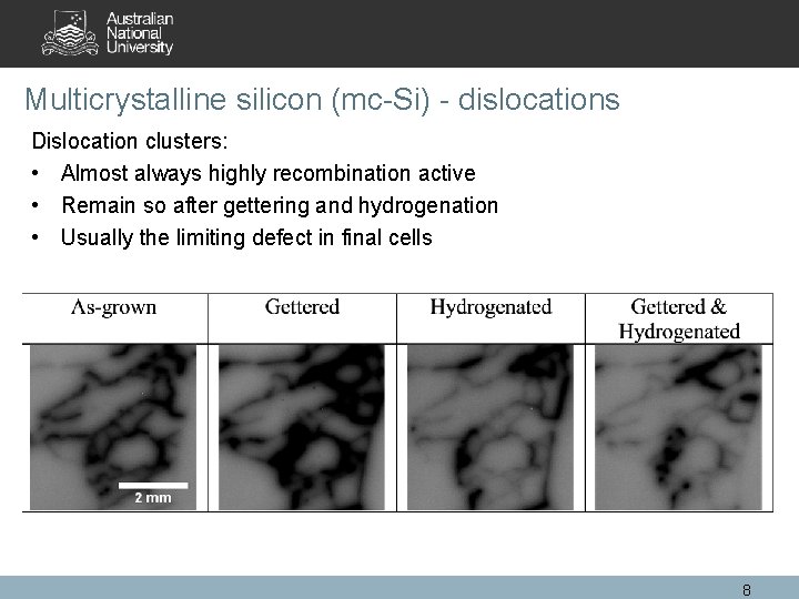
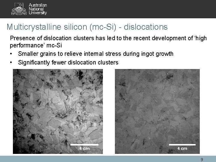
Multicrystalline silicon (mc-Si) - dislocations Dislocation clusters: • Almost always highly recombination active • Remain so after gettering and hydrogenation • Usually the limiting defect in final cells 8

Multicrystalline silicon (mc-Si) - dislocations Presence of dislocation clusters has led to the recent development of ‘high performance’ mc-Si • Smaller grains to relieve internal stress during ingot growth • Significantly fewer dislocation clusters 9

Multicrystalline silicon (mc-Si) – HP mc-Si • GBs much less active in HP mc-Si after processing. • Solves long-standing material problem for mc-Si. • >20% efficiency mc-Si cells in mass production is realistic in next 5 years. 10

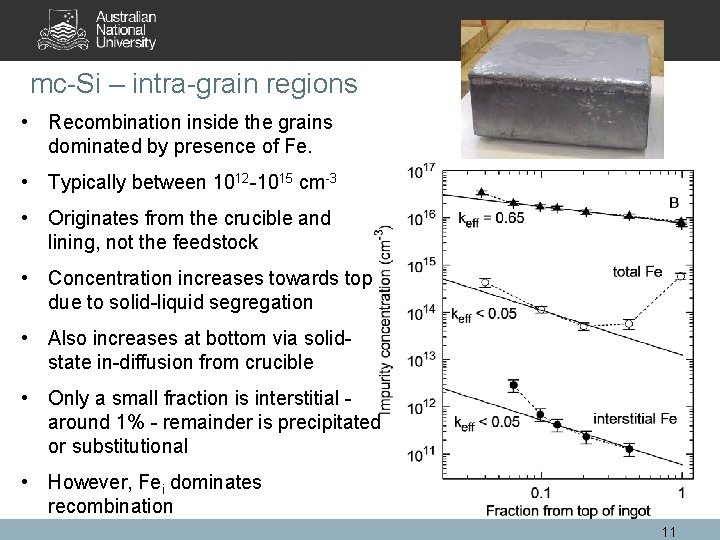
mc-Si – intra-grain regions • Recombination inside the grains dominated by presence of Fe. • Typically between 1012 -1015 cm-3 • Originates from the crucible and lining, not the feedstock • Concentration increases towards top due to solid-liquid segregation • Also increases at bottom via solidstate in-diffusion from crucible • Only a small fraction is interstitial around 1% - remainder is precipitated or substitutional • However, Fei dominates recombination 11

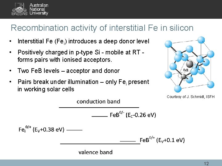
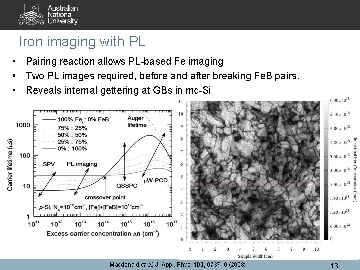
Recombination activity of interstitial Fe in silicon • Interstitial Fe (Fei) introduces a deep donor level • Positively charged in p-type Si - mobile at RT forms pairs with ionised acceptors. • Two Fe. B levels – acceptor and donor • Pairs break under illumination – only Fei present in working solar cells Courtesy of J. Schmidt, ISFH 12

Iron imaging with PL • Pairing reaction allows PL-based Fe imaging • Two PL images required, before and after breaking Fe. B pairs. • Reveals internal gettering at GBs in mc-Si Macdonald et al. J. Appl. Phys. 103, 073710 (2008) 13

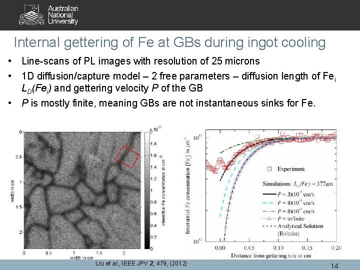
Internal gettering of Fe at GBs during ingot cooling • Line-scans of PL images with resolution of 25 microns • 1 D diffusion/capture model – 2 free parameters – diffusion length of Fei LD(Fei) and gettering velocity P of the GB • P is mostly finite, meaning GBs are not instantaneous sinks for Fe. Liu et al. , IEEE JPV 2, 479, (2012) 14

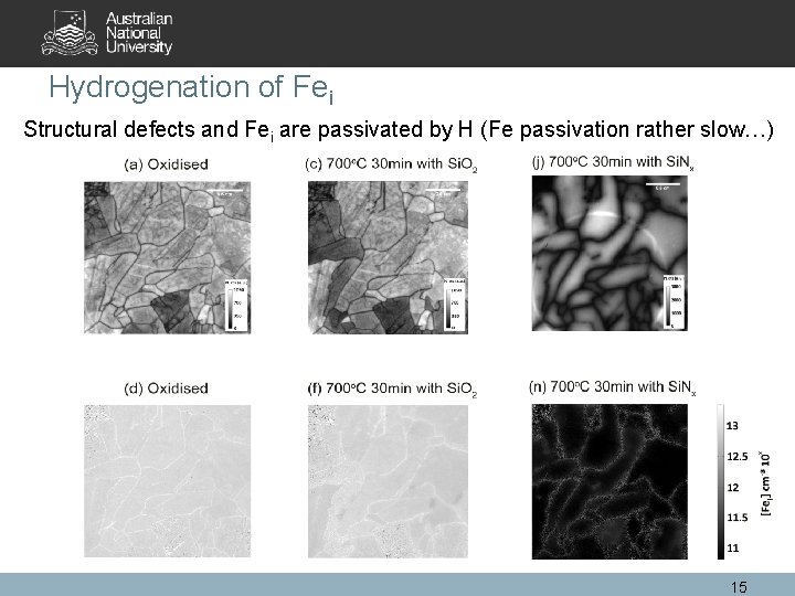
Hydrogenation of Fei Structural defects and Fei are passivated by H (Fe passivation rather slow…) 15

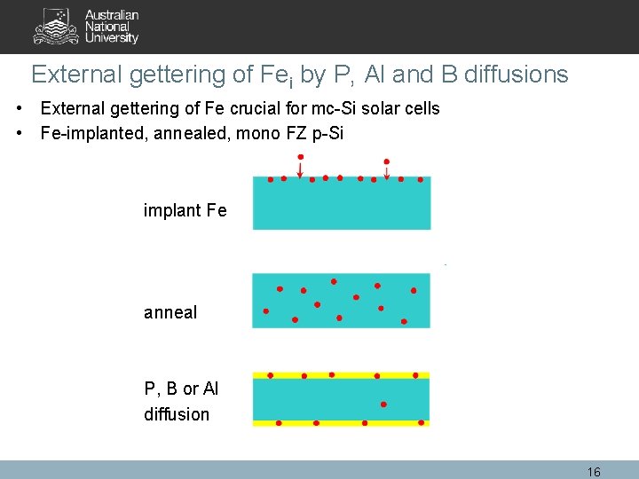
External gettering of Fei by P, Al and B diffusions • External gettering of Fe crucial for mc-Si solar cells • Fe-implanted, annealed, mono FZ p-Si implant Fe anneal P, B or Al diffusion 16

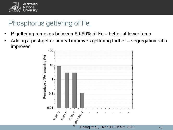
Phosphorus gettering of Fei • P gettering removes between 90 -99% of Fe – better at lower temp • Adding a post-getter anneal improves gettering further – segregation ratio improves Phang et al. , JAP 109, 073521 2011 17

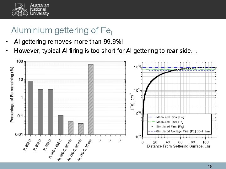
Aluminium gettering of Fei • Al gettering removes more than 99. 9%! • However, typical Al firing is too short for Al gettering to rear side… 18

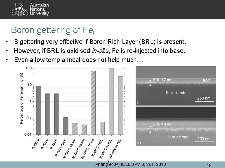
Boron gettering of Fei • B gettering very effective if Boron Rich Layer (BRL) is present. • However, if BRL is oxidised in-situ, Fe is re-injected into base. • Even a low temp anneal does not help much… Phang et al. , IEEE JPV 3, 261, 2013 19

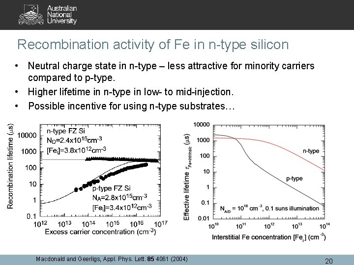
Recombination activity of Fe in n-type silicon • Neutral charge state in n-type – less attractive for minority carriers compared to p-type. • Higher lifetime in n-type in low- to mid-injection. • Possible incentive for using n-type substrates… Macdonald and Geerligs, Appl. Phys. Lett. 85 4061 (2004) 20

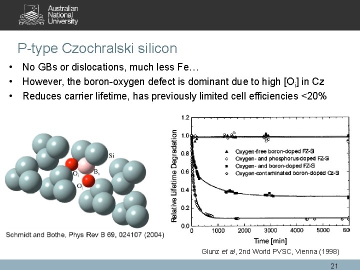
P-type Czochralski silicon • No GBs or dislocations, much less Fe… • However, the boron-oxygen defect is dominant due to high [Oi] in Cz • Reduces carrier lifetime, has previously limited cell efficiencies <20% Glunz et al, 2 nd World PVSC, Vienna (1998) 21

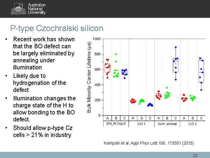
P-type Czochralski silicon • Recent work has shown that the BO defect can be largely eliminated by annealing under illumination • Likely due to hydrogenation of the defect • Illumination changes the charge state of the H to allow bonding to the BO defect. • Should allow p-type Cz cells > 21% in industry Nampalli et al, Appl Phys Lett 106, 173501 (2015) 22

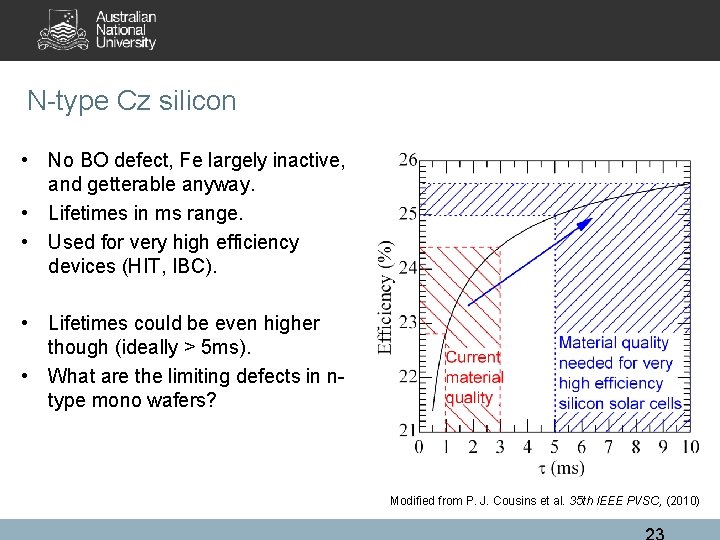
N-type Cz silicon • No BO defect, Fe largely inactive, and getterable anyway. • Lifetimes in ms range. • Used for very high efficiency devices (HIT, IBC). • Lifetimes could be even higher though (ideally > 5 ms). • What are the limiting defects in ntype mono wafers? Modified from P. J. Cousins et al. 35 th IEEE PVSC, (2010)

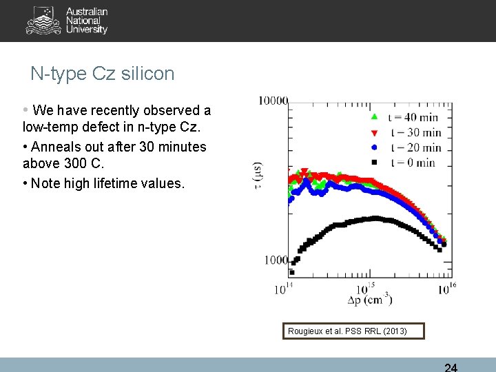
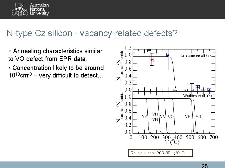
N-type Cz silicon • We have recently observed a low-temp defect in n-type Cz. • Anneals out after 30 minutes above 300 C. • Note high lifetime values. Rougieux et al. PSS RRL (2013)

N-type Cz silicon - vacancy-related defects? • Annealing characteristics similar to VO defect from EPR data. • Concentration likely to be around 1010 cm-3 – very difficult to detect… Rougieux et al. PSS RRL (2013)

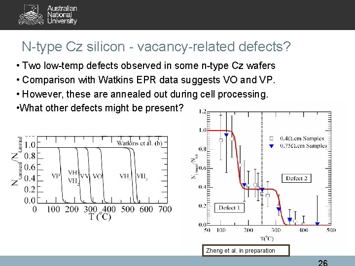
N-type Cz silicon - vacancy-related defects? • Two low-temp defects observed in some n-type Cz wafers • Comparison with Watkins EPR data suggests VO and VP. • However, these are annealed out during cell processing. • What other defects might be present? Zheng et al. in preparation

Conclusions • Multicrystalline silicon dominated by: • Grain boundaries – can be partly hydrogenated • Dislocation clusters – not present in ‘high performance’ mc-Si • Dissolved Fe – removed by gettering • P-type Cz silicon limited by: • Boron-oxygen defect – can be eliminated by charge-state controlled hydrogenation • N-type Cz silicon: • Possibly affected by vacancy-related defects – but these are annealed out • Silicon material quality is still improving dramatically… a moving target 27

Thank you! We gratefully acknowledge the support of the Australian Renewable Energy Agency (ARENA) through Project RND 009, and the Australian Research Council.