Defect Material Characterization 5 Years Work Plan RD
- Slides: 20

Defect & Material Characterization 5 Years Work Plan RD 50 November 2018 - M. Moll -1 -

Work Plan: Material & Defect Characterization • Activities: Material and Defect Characterization § Detection and microscopic characterization of standard and material engineered silicon via dedicated techniques (DLTS, TSC, TDRC, SIMS, ICP-MS, PITS, FTIR, TCT, EPR, HRTEM) § Identification of electrically active defects induced by irradiation responsible for trapping, leakage current, change of Neff , change of E-Field § Studying possible application for radiation hardening § Deliver input for device simulations (e. g. TCAD) to predict detector performance under various conditions RD 50 November 2018 - M. Moll -2 -

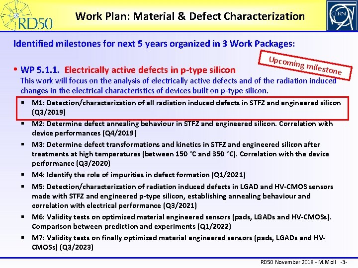
Work Plan: Material & Defect Characterization Identified milestones for next 5 years organized in 3 Work Packages: • WP 5. 1. 1. Electrically active defects in p-type silicon Upcom in g miles tone This work will focus on the analysis of electrically active defects and of the radiation induced changes in the electrical characteristics of devices built on p-type silicon. § M 1: Detection/characterization of all radiation induced defects in STFZ and engineered silicon § § § (Q 3/2019) M 2: Determine defect annealing behaviour in STFZ and engineered silicon. Correlation with device performances (Q 4/2019) M 3: Determine defect transformations and kinetics in STFZ and engineered silicon after treatments at high temperatures (between 150 °C and 350 °C). Correlation with the device performance (Q 3/2020) M 4: Identify the role of impurities in defect formation (Q 1/2021) M 5: Detection/characterization of radiation induced defects in LGAD and HV-CMOS sensors made with STFZ and engineered p-type silicon, establishing annealing behaviour and correlation with electrical performance (Q 3/2021) M 6: Validity tests on optimized material engineered sensors (pads, LGADs and HV-CMOSs). Comparison between prediction and experiments (Q 1/2022) M 7: Validity tests on finally optimized material engineered sensors (pads, LGADs and HVCMOSs) (Q 3/2023) RD 50 November 2018 - M. Moll -3 -

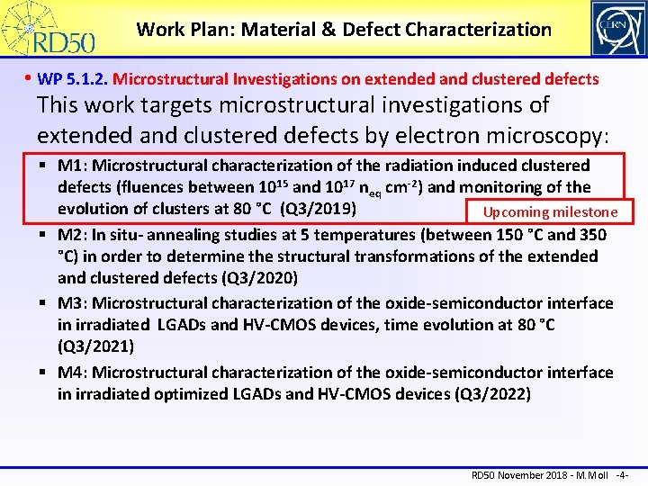
Work Plan: Material & Defect Characterization • WP 5. 1. 2. Microstructural Investigations on extended and clustered defects This work targets microstructural investigations of extended and clustered defects by electron microscopy: § M 1: Microstructural characterization of the radiation induced clustered defects (fluences between 1015 and 1017 neq cm-2) and monitoring of the evolution of clusters at 80 °C (Q 3/2019) Upcoming milestone § M 2: In situ- annealing studies at 5 temperatures (between 150 °C and 350 °C) in order to determine the structural transformations of the extended and clustered defects (Q 3/2020) § M 3: Microstructural characterization of the oxide-semiconductor interface in irradiated LGADs and HV-CMOS devices, time evolution at 80 °C (Q 3/2021) § M 4: Microstructural characterization of the oxide-semiconductor interface in irradiated optimized LGADs and HV-CMOS devices (Q 3/2022) RD 50 November 2018 - M. Moll -4 -

Work Plan: Material & Defect Characterization • WP 5. 1. 3 Theory of defects and defect kinetics modelling § M 1: Modelling of the detected defect generation/kinetics and of the impact on the device performance corresponding to annealing treatments at 80 °C (Q 3/2020) § M 2: Modelling of the detected defect generation/kinetics and of the impact on the device performance corresponding to annealing at temperatures between 150 °C and 350 °C and final assessment of the role of the intentional added impurities (Q 1/2021) § M 3: Identification of the optimal impurity concentrations for pads, LGADs and HV-CMOSs as input for production. (Q 3/2021) § M 4: Improvements of the developed models according to validity test foreseen as 5. 1. 1 -M 6 and provide new optimization solutions for 5. 1. 1 -M 7. (Q 3/2022) § M 5: Validity test for the developed theoretical models based on the results obtained on 5. 1. 1 -M 7 optimized sensors (Q 3/2023) RD 50 November 2018 - M. Moll -5 -

Defect & Material Characterization This Workshop RD 50 November 2018 - M. Moll -6 -

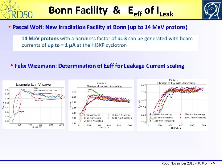
Bonn Facility & Eeff of ILeak • Pascal Wolf: New Irradiation Facility at Bonn (up to 14 Me. V protons) • Felix Wizemann: Determination of Eeff for Leakage Current scaling RD 50 November 2018 - M. Moll -7 -

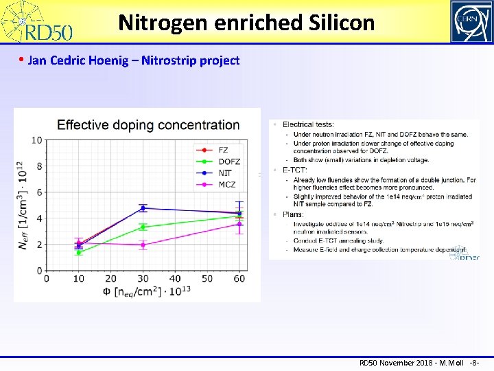
Nitrogen enriched Silicon • Jan Cedric Hoenig – Nitrostrip project RD 50 November 2018 - M. Moll -8 -

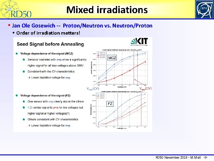
Mixed irradiations • Jan Ole Gosewich -- Proton/Neutron vs. Neutron/Proton § Order of irradiation matters! RD 50 November 2018 - M. Moll -9 -

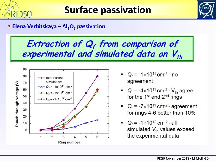
Surface passivation • Elena Verbitskaya – Al 2 O 3 passivation RD 50 November 2018 - M. Moll -10 -

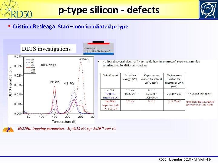
p-type silicon - defects • Cristina Besleaga Stan – non irradiated p-type RD 50 November 2018 - M. Moll -11 -

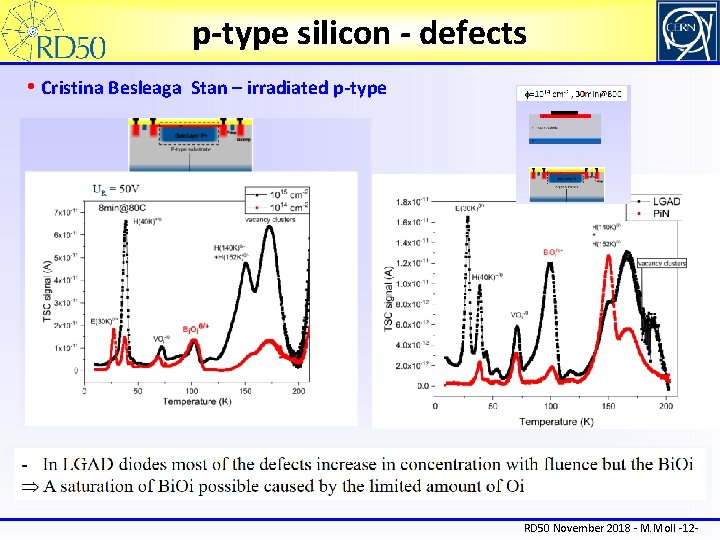
p-type silicon - defects • Cristina Besleaga Stan – irradiated p-type RD 50 November 2018 - M. Moll -12 -

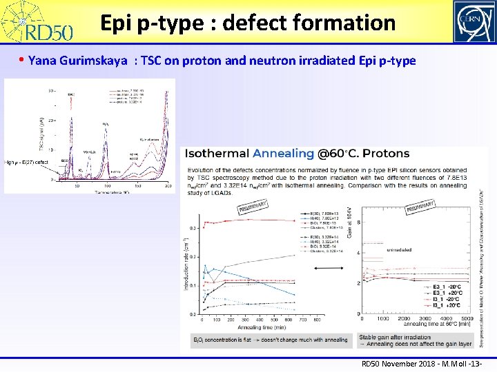
Epi p-type : defect formation • Yana Gurimskaya : TSC on proton and neutron irradiated Epi p-type RD 50 November 2018 - M. Moll -13 -

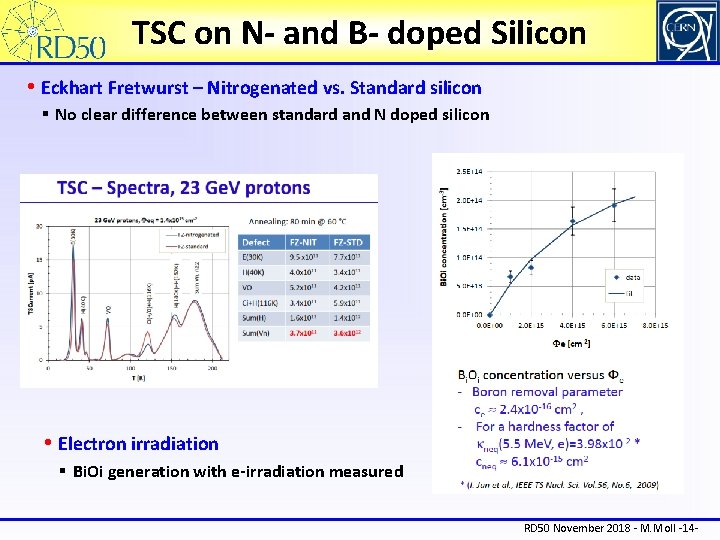
TSC on N- and B- doped Silicon • Eckhart Fretwurst – Nitrogenated vs. Standard silicon § No clear difference between standard and N doped silicon • Electron irradiation § Bi. Oi generation with e-irradiation measured RD 50 November 2018 - M. Moll -14 -

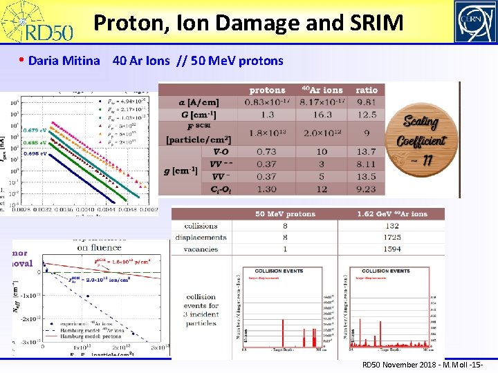
Proton, Ion Damage and SRIM • Daria Mitina 40 Ar Ions // 50 Me. V protons RD 50 November 2018 - M. Moll -15 -

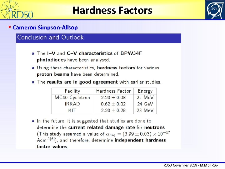
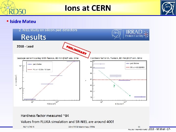
Hardness Factors • Cameron Simpson-Allsop RD 50 November 2018 - M. Moll -16 -

Ions at CERN • Isidre Mateu RD 50 November 2018 - M. Moll -17 -

Defect & Material Characterization Discussion RD 50 November 2018 - M. Moll -18 -

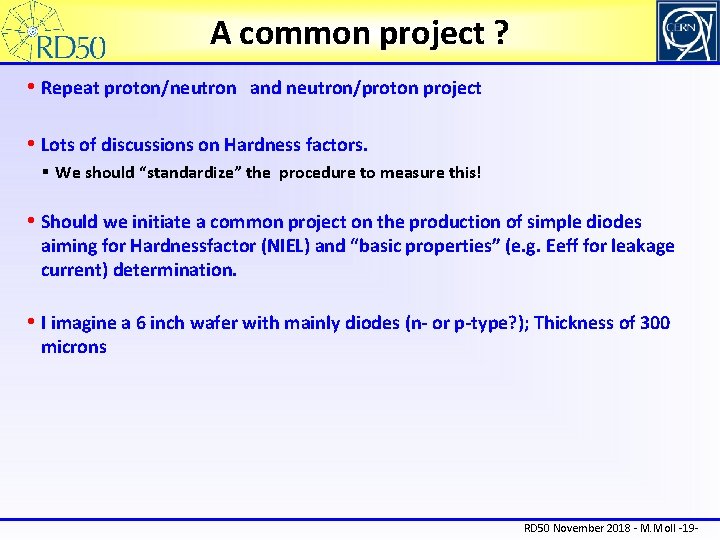
A common project ? • Repeat proton/neutron and neutron/proton project • Lots of discussions on Hardness factors. § We should “standardize” the procedure to measure this! • Should we initiate a common project on the production of simple diodes aiming for Hardnessfactor (NIEL) and “basic properties” (e. g. Eeff for leakage current) determination. • I imagine a 6 inch wafer with mainly diodes (n- or p-type? ); Thickness of 300 microns RD 50 November 2018 - M. Moll -19 -

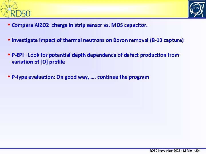
• Compare Al 2 O 2 charge in strip sensor vs. MOS capacitor. • Investigate impact of thermal neutrons on Boron removal (B-10 capture) • P-EPI : Look for potential depth dependence of defect production from variation of [O] profile • P-type evaluation: On good way, …. continue the program RD 50 November 2018 - M. Moll -20 -