Deep Nwell CMOS MAPS and hybrid pixels in
Deep N-well CMOS MAPS and hybrid pixels in vertical integration technology for the Super. B SVT L. Rattia for the VIPIX collaboration Pixel systems for thin charged particle trackers based on vertical integration technologies a Università Super. B Workshop IX June 16 -20 2009 Perugia , Italy degli Studi di Pavia and INFN Pavia
SVT layer 0 options for Super. B Design of the SVT layer 0 at Super. B has to comply with severe requirements large background, >5 MHz, small thickness, <0. 5 X 0 Striplets Hybrid pixel detectors presently the baseline solution for the TDR submission of a 130 nm CMOS front-end chip planned for September (see talk by G. Traversi ) fine pitch (50 μ m) bump bonding (IZM, Munich) with a 200 μ m thick pixel detector (FBK- irst, Trento) Deep N-well CMOS monolithic sensors (DNW-MAPS) extensive R&D ongoing in a 130 nm CMOS process ( Apsel and SDR families), Apsel 4 D tested on the PS beam at CERN in September 2008 can be easily made compatible with low material budget requirements innovative approach (deep N-well sensor) proposed to enable fast readout through pixel-level sparsification and time stamping L. Ratti, “DNW CMOS MAPS and hybrid pixels in 3 D technology”, Super. B Workshop IX
3 DIC Consortium Includes FNAL and Italian and French Institutions (also Bonn and AGH Universities, see http: //3 dic. fnal. gov ) aiming to work together on a MPW run using the Tezzaron 3 D IC fabrication process The collaborating institutions are willing to share information on design tools and design rule implementation, cell libraries, circuit blocks (besides costs) The Consortium has made a considerable effort to meet the deadline of end of May ’ 09 for a multiproject run in the Tezzaron /Chartered 130 nm technology As far as the Italian contribution is concerned, this first submission, funded in the frame of the P-ILC experiment (INFN), includes 3 D MAPS sensors mainly for applications to the ILC, but also some vertically integrated structures aimed at vtx applications to the Super. B Factory L. Ratti, “DNW CMOS MAPS and hybrid pixels in 3 D technology”, Super. B Workshop IX
Outline Deep N-well (DNW) MAPS working principle and features Vertical integration (or 3 D) technologies and the Tezzaron /Chartered process DNW MAPS in 3 D CMOS technology: Apsel MAPS 3 D version From 2 D to 3 D Analog FE design features and expected performance Charge collection efficiency improvement through 3 D processes Hybrid pixels with 3 D FE chip (3 D hybrid pixels) 3 D FE for a pixel detector in XFAB technology Conclusion and future plans L. Ratti, “DNW CMOS MAPS and hybrid pixels in 3 D technology”, Super. B Workshop IX
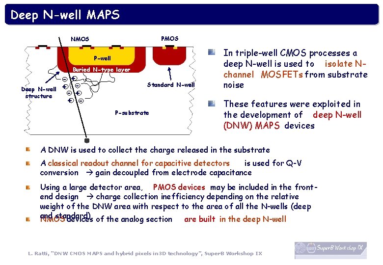
Deep N-well MAPS PMOS NMOS P-well Buried N-type layer Deep N-well structure - + + - Standard N-well P-substrate In triple-well CMOS processes a deep N-well is used to isolate Nchannel MOSFETs from substrate noise These features were exploited in the development of deep N-well (DNW) MAPS devices A DNW is used to collect the charge released in the substrate A classical readout channel for capacitive detectors is used for Q-V conversion gain decoupled from electrode capacitance Using a large detector area, PMOS devices may be included in the frontend design charge collection inefficiency depending on the relative weight of the DNW area with respect to the area of all the N-wells (deep and standard) NMOS devices of the analog section are built in the deep N-well L. Ratti, “DNW CMOS MAPS and hybrid pixels in 3 D technology”, Super. B Workshop IX
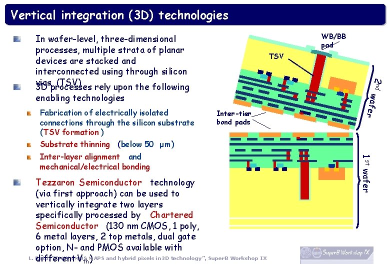
Vertical integration (3 D) technologies WB/BB pad In wafer-level, three-dimensional processes, multiple strata of planar devices are stacked and interconnected using through silicon vias (TSV) 3 D processes rely upon the following enabling technologies 2 nd Inter-tier bond pads wafe r Fabrication of electrically isolated connections through the silicon substrate (TSV formation ) TSV Substrate thinning (below 50 μ m) Tezzaron Semiconductor technology (via first approach) can be used to vertically integrate two layers specifically processed by Chartered Semiconductor (130 nm CMOS, 1 poly, 6 metal layers, 2 top metals, dual gate option, N- and PMOS available with L. Ratti, “DNW CMOS and hybrid pixels in 3 D technology”, Super. B Workshop IX different V th. MAPS ) 1 st wafer Inter-layer alignment and mechanical/electrical bonding
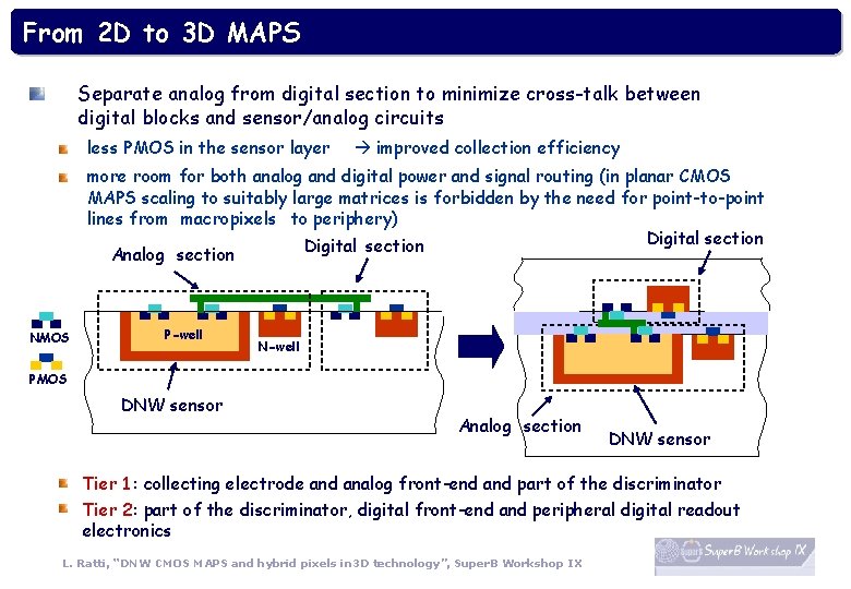
From 2 D to 3 D MAPS Separate analog from digital section to minimize cross-talk between digital blocks and sensor/analog circuits less PMOS in the sensor layer improved collection efficiency more room for both analog and digital power and signal routing (in planar CMOS MAPS scaling to suitably large matrices is forbidden by the need for point-to-point lines from macropixels to periphery) Digital section Analog section NMOS P-well N-well PMOS DNW sensor Analog section DNW sensor Tier 1 : collecting electrode and analog front-end and part of the discriminator Tier 2: part of the discriminator, digital front-end and peripheral digital readout electronics L. Ratti, “DNW CMOS MAPS and hybrid pixels in 3 D technology”, Super. B Workshop IX
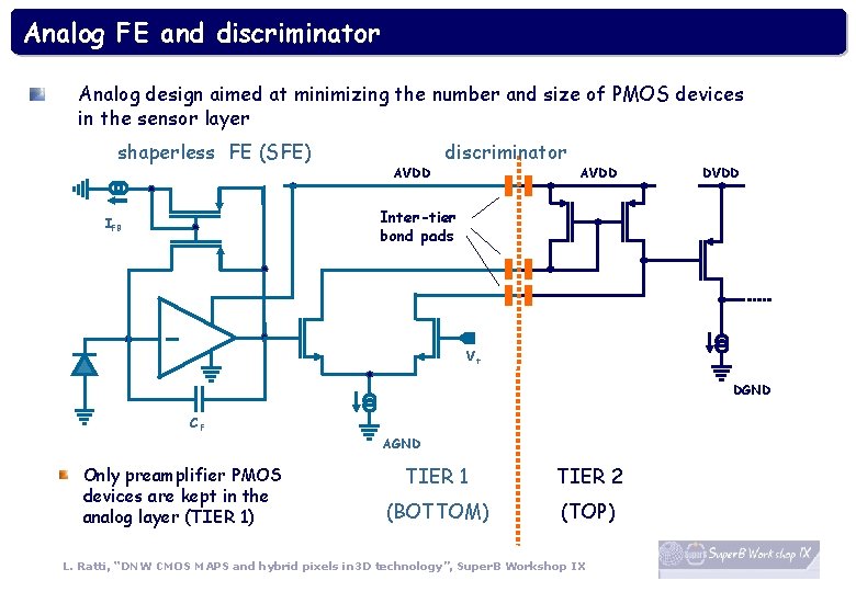
Analog FE and discriminator Analog design aimed at minimizing the number and size of PMOS devices in the sensor layer shaperless FE (SFE) AVDD discriminator AVDD DVDD Inter-tier bond pads IFB Vt DGND CF AGND Only preamplifier PMOS devices are kept in the analog layer (TIER 1) TIER 1 TIER 2 (BOTTOM) (TOP) L. Ratti, “DNW CMOS MAPS and hybrid pixels in 3 D technology”, Super. B Workshop IX
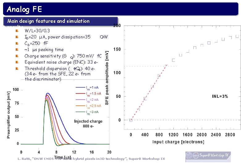
Analog FE Main design features and simulation results W/L=30/0. 3 ID =20 μA, power dissipation=35 m. W C D =250 f. F ~1 ms peaking time Charge sensitivity (G Q): 750 m. V/ f. C Equivalent noise charge (ENC): 33 e. Threshold dispersion ( DQt): 40 e(34 e- from the SFE, 22 e- from the discriminator) L. Ratti, “DNW CMOS MAPS and hybrid pixels in 3 D technology”, Super. B Workshop IX
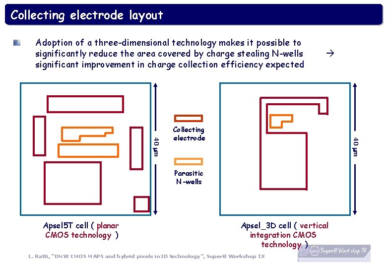
Collecting electrode layout Adoption of a three-dimensional technology makes it possible to significantly reduce the area covered by charge stealing N-wells significant improvement in charge collection efficiency expected 40 mm Collecting electrode Parasitic N-wells Apsel 5 T cell ( planar CMOS technology ) Apsel_3 D cell ( vertical integration CMOS technology ) L. Ratti, “DNW CMOS MAPS and hybrid pixels in 3 D technology”, Super. B Workshop IX
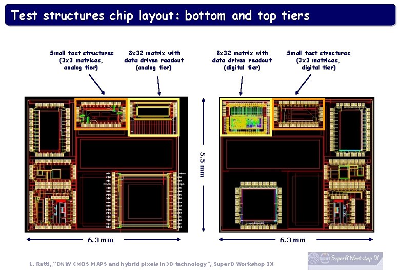
Test structures chip layout: bottom and top tiers Small test structures (3 x 3 matrices, analog tier) 8 x 32 matrix with data driven readout (digital tier) Small test structures (3 x 3 matrices, digital tier) 5. 5 mm 6. 3 mm L. Ratti, “DNW CMOS MAPS and hybrid pixels in 3 D technology”, Super. B Workshop IX 6. 3 mm
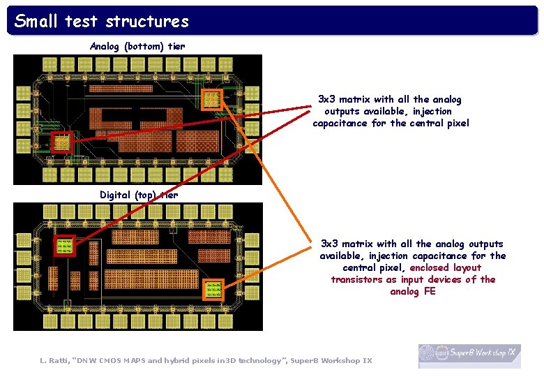
Small test structures Analog (bottom) tier 3 x 3 matrix with all the analog outputs available, injection capacitance for the central pixel Digital (top) tier 3 x 3 matrix with all the analog outputs available, injection capacitance for the central pixel, enclosed layout transistors as input devices of the analog FE L. Ratti, “DNW CMOS MAPS and hybrid pixels in 3 D technology”, Super. B Workshop IX
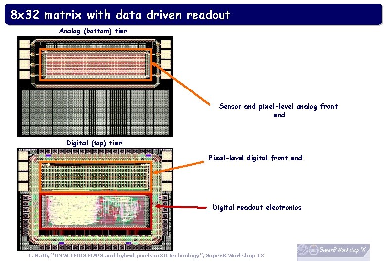
8 x 32 matrix with data driven readout Analog (bottom) tier Sensor and pixel-level analog front end Digital (top) tier Pixel-level digital front end Digital readout electronics L. Ratti, “DNW CMOS MAPS and hybrid pixels in 3 D technology”, Super. B Workshop IX

3 D hybrid pixels Development of a 3 D front-end chip to be vertically integrated with fully depleted detectors through some more (bump bonding) or less (direct bonding) standard technique 1 st layer Bump bonding (e. g. IZM) 2 nd layer Digital section Analog section detector layer 1 st layer 2 nd layer detector layer Larger signal available from the detector More advantageous trade-off between S/N and dissipated power L. Ratti, “DNW CMOS MAPS and hybrid pixels in 3 D technology”, Super. B Workshop IX Direct bonding (e. g. Ziptronix )
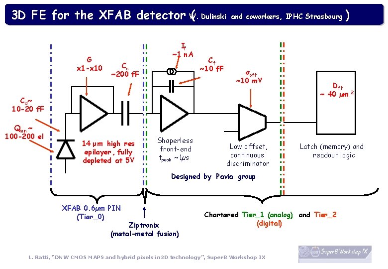
3 D FE for the XFAB detector W. ( Dulinski G x 1 -x 10 If ~1 n. A Cc ~200 f. F Cf ~10 f. F and coworkers, IPHC Strasbourg σ off ~10 m. V C d~ 10 -20 f. F Qmin ~ 100 -200 el 14 μ m high res epilayer , fully depleted at 5 V Shaperless front-end tpeak ~1µs Low offset, continuous discriminator D ff ~ 40 µm Ziptronix (metal-metal fusion) Chartered Tier_1 (analog) and Tier_2 (digital) L. Ratti, “DNW CMOS MAPS and hybrid pixels in 3 D technology”, Super. B Workshop IX 2 Latch (memory) and readout logic Designed by Pavia group XFAB 0. 6µm PIN (Tier_0) )
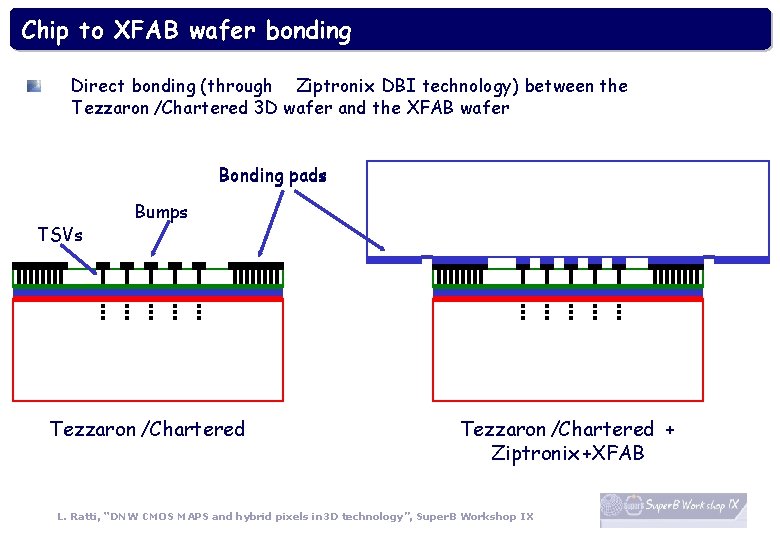
Chip to XFAB wafer bonding Direct bonding (through Ziptronix DBI technology) between the Tezzaron /Chartered 3 D wafer and the XFAB wafer Bonding pads TSVs Bumps Tezzaron /Chartered + Ziptronix +XFAB L. Ratti, “DNW CMOS MAPS and hybrid pixels in 3 D technology”, Super. B Workshop IX
Conclusion and future plans Two different 3 D solutions are being investigated for the SVT layer 0 at Super. B through extensive R&D programs, namely hybrid pixel detectors and DNW MAPS, both in 130 nm CMOS technology Both MAPS and hybrid pixels can gain significant benefits from going 3 D increase in charge collection efficiency immunity from (or reduction of) cross-talk phenomena between digital blocks and sensor/analog circuits scalability to large sensor matrices better trade-off between point resolution and functional density The hybrid pixel approach is expected to guarantee superior performance as far as the trade-off between S/N and power dissipation is concerned Test of the first 3 D MAPS sensors expected to start next September Design of a vertically integrated large (~256 x 256) DNW MAPS detector with data driven readout architecture and of a 3 D FE chip for hybrid pixels is planned for the beginning of next year L. Ratti, “DNW CMOS MAPS and hybrid pixels in 3 D technology”, Super. B Workshop IX

Backup slides
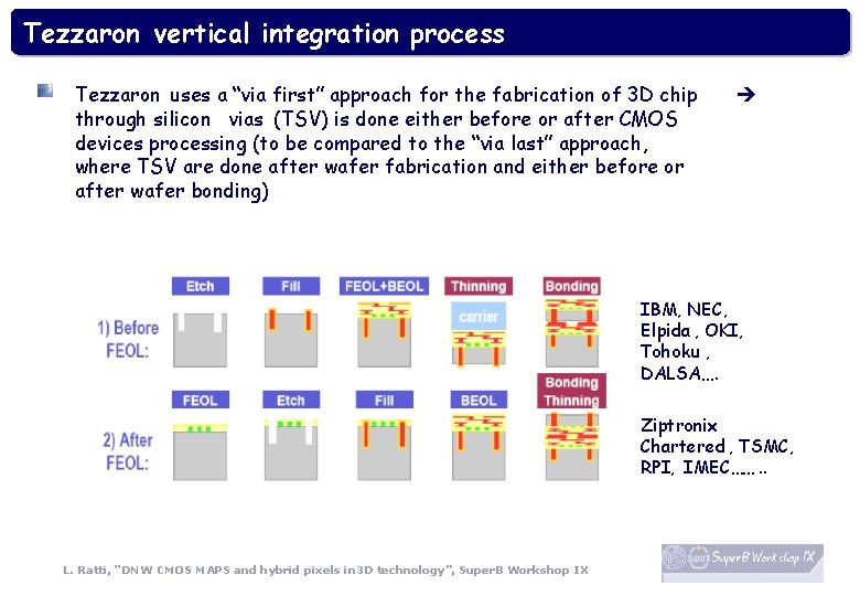
Tezzaron vertical integration process Tezzaron uses a “via first” approach for the fabrication of 3 D chip through silicon vias (TSV) is done either before or after CMOS devices processing (to be compared to the “via last” approach, where TSV are done after wafer fabrication and either before or after wafer bonding) IBM, NEC, Elpida , OKI, Tohoku , DALSA…. Ziptronix Chartered , TSMC, RPI, IMEC……. . L. Ratti, “DNW CMOS MAPS and hybrid pixels in 3 D technology”, Super. B Workshop IX
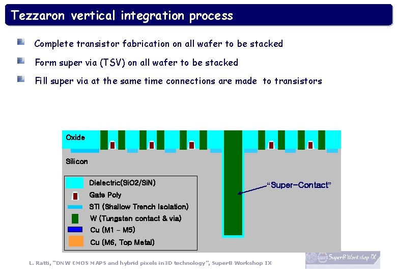
Tezzaron vertical integration process Complete transistor fabrication on all wafer to be stacked Form super via (TSV) on all wafer to be stacked Fill super via at the same time connections are made to transistors Oxide Silicon Dielectric(Si. O 2/Si. N) “Super-Contact” Gate Poly STI (Shallow Trench Isolation) W (Tungsten contact & via) Cu (M 1 – M 5) Cu (M 6, Top Metal) L. Ratti, “DNW CMOS MAPS and hybrid pixels in 3 D technology”, Super. B Workshop IX
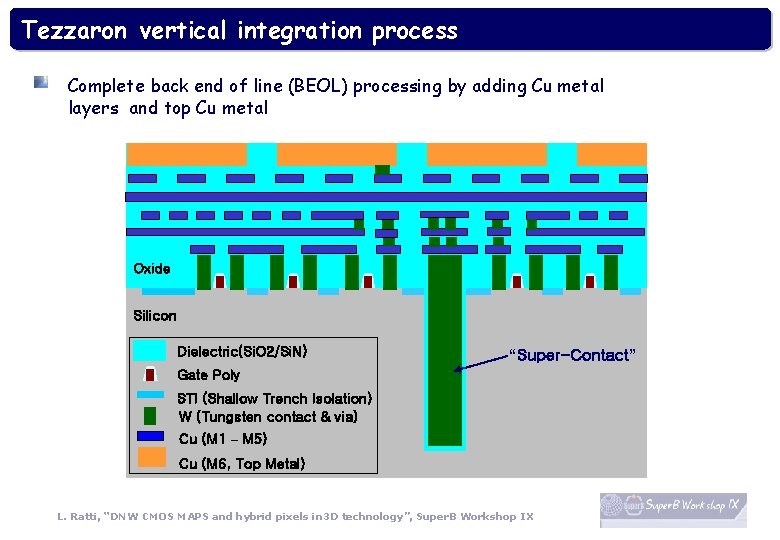
Tezzaron vertical integration process Complete back end of line (BEOL) processing by adding Cu metal layers and top Cu metal Oxide Silicon Dielectric(Si. O 2/Si. N) “Super-Contact” Gate Poly STI (Shallow Trench Isolation) W (Tungsten contact & via) Cu (M 1 – M 5) Cu (M 6, Top Metal) L. Ratti, “DNW CMOS MAPS and hybrid pixels in 3 D technology”, Super. B Workshop IX
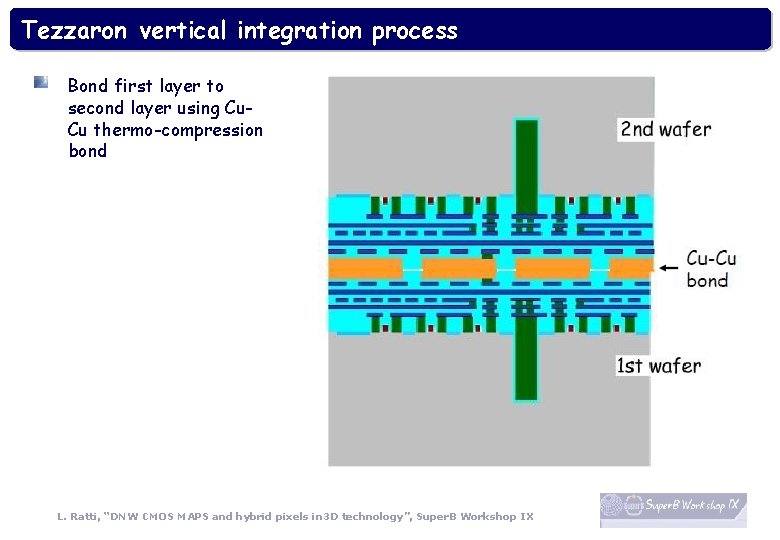
Tezzaron vertical integration process Bond first layer to second layer using Cu. Cu thermo-compression bond L. Ratti, “DNW CMOS MAPS and hybrid pixels in 3 D technology”, Super. B Workshop IX
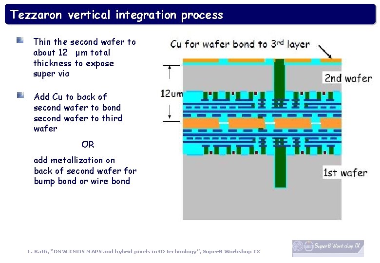
Tezzaron vertical integration process Thin the second wafer to about 12 μ m total thickness to expose super via Add Cu to back of second wafer to bond second wafer to third wafer OR add metallization on back of second wafer for bump bond or wire bond L. Ratti, “DNW CMOS MAPS and hybrid pixels in 3 D technology”, Super. B Workshop IX
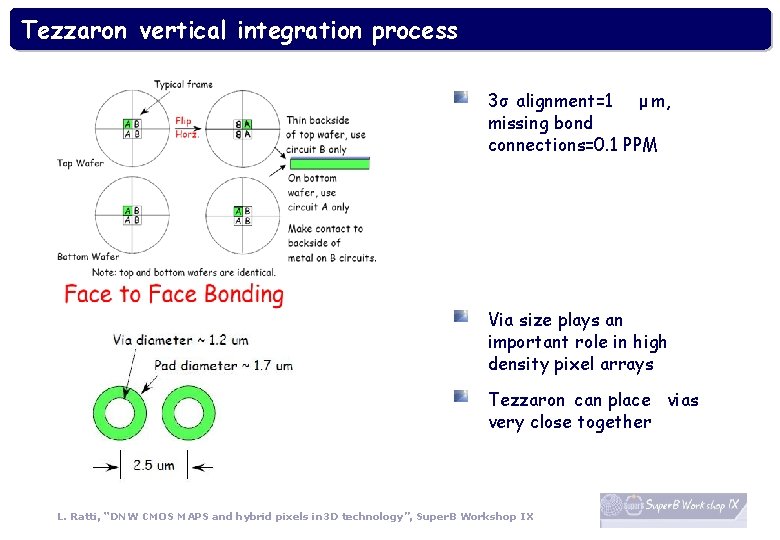
Tezzaron vertical integration process 3σ alignment=1 μ m, missing bond connections=0. 1 PPM Via size plays an important role in high density pixel arrays Tezzaron can place vias very close together L. Ratti, “DNW CMOS MAPS and hybrid pixels in 3 D technology”, Super. B Workshop IX
- Slides: 24