DDR PHY Offering Q 2 2016 v 5

- Slides: 9

DDR PHY Offering Q 2 2016 v 5

Introduction § ARM spin-off AMS IP company § Located in Bangalore, India § Established Nov’ 2013 § Owns copyrights of ARM DDR PHY DB and patents § Design maturity in IPs in spite of being new company § Healthy and profitable small company § World wide happy customers § Partnership with multiple foundries § 100% track record of first time working IPs § Innovation driven : 5 provisional patents in DDR confidential

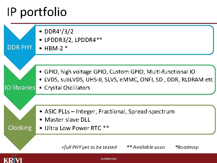
IP portfolio • DDR 4+/3/2 • LPDDR 3/2, LPDDR 4** DDR PHY • HBM-2 * • GPIO, high voltage GPIO, Custom GPIO, Multi-functional IO • LVDS, sub. LVDS, UHS-II, SLVS, e. MMC, ONFI, SD , DDR, RLDRAM etc IO libraries • Crystal Oscillators Clocking • ASIC PLLs – Integer, Fractional, Spread-spectrum • Master slave DLL • Ultra Low Power RTC ** +full PHY yet to be tested confidential ** Available soon *Roadmap

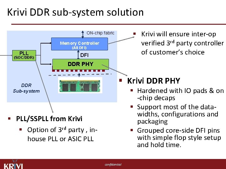
Krivi DDR sub-system solution § Krivi will ensure inter-op verified 3 rd party controller of customer’s choice ON-chip fabric Memory Controller (All DFI) PLL (SOC/DDR) DFI DDR PHY DDR Sub-system § Krivi DDR PHY § Hardened with IO pads & on -chip decaps § Support most of the datawidths, configurations and packaging § Grouped core-side DFI pins with simple flop style setup and hold time. § PLL/SSPLL from Krivi § Option of 3 rd party , inhouse PLL or ASIC PLL confidential

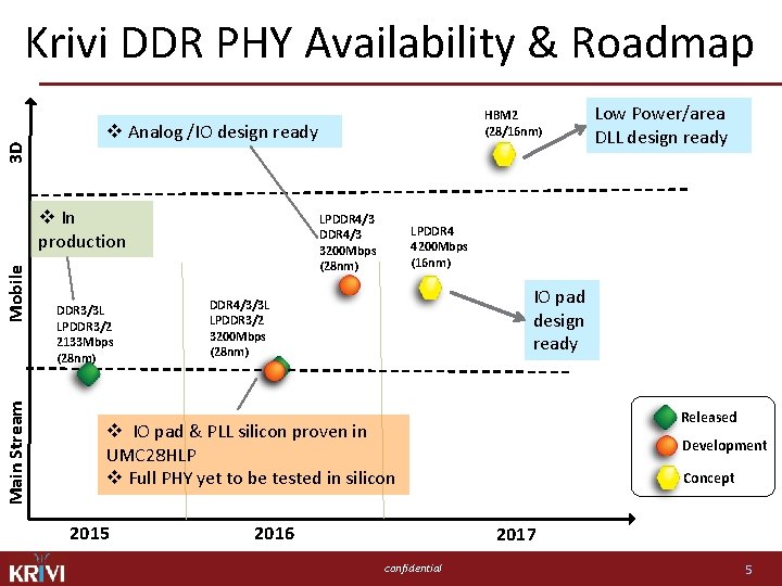
3 D Krivi DDR PHY Availability & Roadmap v Analog /IO design ready Mobile v In production Main Stream HBM 2 (28/16 nm) DDR 3/3 L LPDDR 3/2 2133 Mbps (28 nm) LPDDR 4/3 3200 Mbps (28 nm) LPDDR 4 4200 Mbps (16 nm) IO pad design ready DDR 4/3/3 L LPDDR 3/2 3200 Mbps (28 nm) Released v IO pad & PLL silicon proven in UMC 28 HLP v Full PHY yet to be tested in silicon 2015 Low Power/area DLL design ready 2016 Development Concept 2017 confidential 5

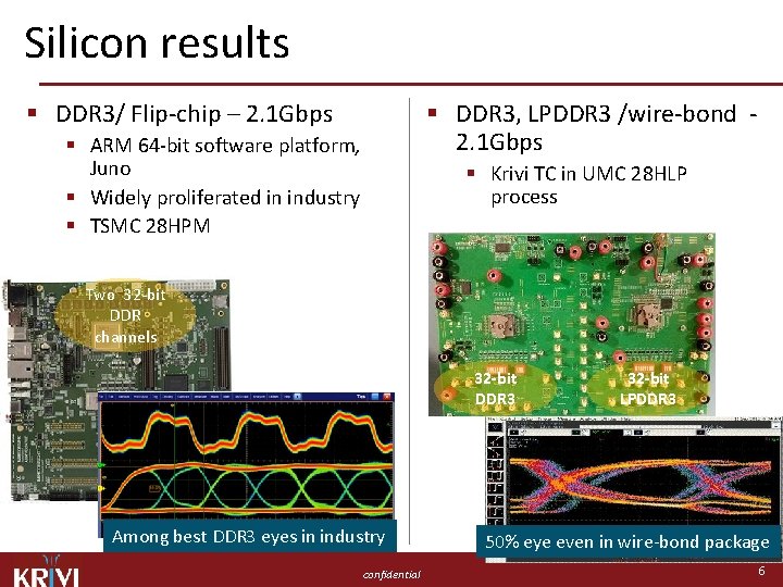
Silicon results § DDR 3/ Flip-chip – 2. 1 Gbps § DDR 3, LPDDR 3 /wire-bond 2. 1 Gbps § ARM 64 -bit software platform, Juno § Widely proliferated in industry § TSMC 28 HPM § Krivi TC in UMC 28 HLP process Two 32 -bit DDR channels 32 -bit DDR 3 Among best DDR 3 eyes in industry confidential 32 -bit LPDDR 3 50% eye even in wire-bond package 6

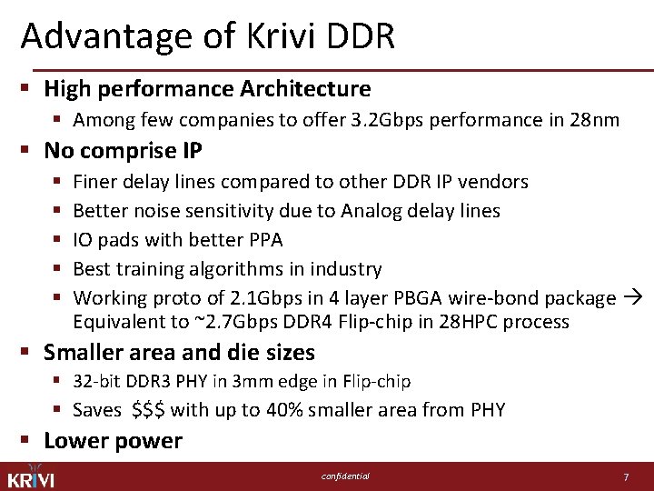
Advantage of Krivi DDR § High performance Architecture § Among few companies to offer 3. 2 Gbps performance in 28 nm § No comprise IP § § § Finer delay lines compared to other DDR IP vendors Better noise sensitivity due to Analog delay lines IO pads with better PPA Best training algorithms in industry Working proto of 2. 1 Gbps in 4 layer PBGA wire-bond package Equivalent to ~2. 7 Gbps DDR 4 Flip-chip in 28 HPC process § Smaller area and die sizes § 32 -bit DDR 3 PHY in 3 mm edge in Flip-chip § Saves $$$ with up to 40% smaller area from PHY § Lower power confidential 7

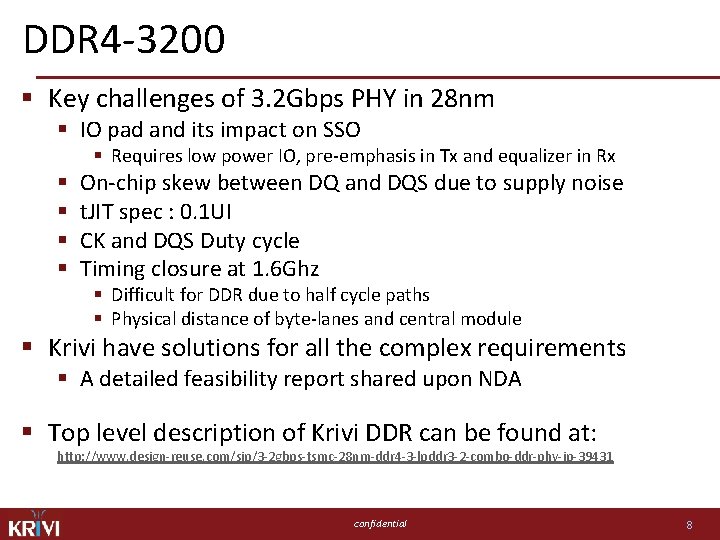
DDR 4 -3200 § Key challenges of 3. 2 Gbps PHY in 28 nm § IO pad and its impact on SSO § Requires low power IO, pre-emphasis in Tx and equalizer in Rx § § On-chip skew between DQ and DQS due to supply noise t. JIT spec : 0. 1 UI CK and DQS Duty cycle Timing closure at 1. 6 Ghz § Difficult for DDR due to half cycle paths § Physical distance of byte-lanes and central module § Krivi have solutions for all the complex requirements § A detailed feasibility report shared upon NDA § Top level description of Krivi DDR can be found at: http: //www. design-reuse. com/sip/3 -2 gbps-tsmc-28 nm-ddr 4 -3 -lpddr 3 -2 -combo-ddr-phy-ip-39431 confidential 8
