DDR 333 The New Wave Bill Gervasi Technology

DDR 333 – The New Wave Bill Gervasi Technology Analyst, Transmeta Corporation Chairman, JEDEC Memory Parametrics Confidential and Proprietary Information
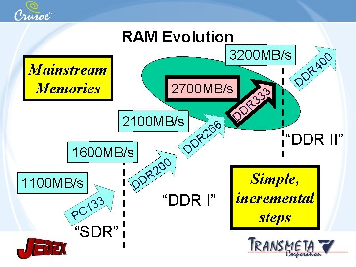
RAM Evolution 3200 MB/s Mainstream Memories 2700 MB/s 2100 MB/s 1600 MB/s 1100 MB/s D 0 0 2 R D 3 3 1 C 6 6 R 2 DD “DDR I” P “SDR” Confidential and Proprietary Information 3 3 R 3 0 0 4 R D D DD “DDR II” Simple, incremental steps
Key to System Evolution Never over-design! Implement just enough new features to achieve incremental improvements Use low cost high volume infrastructure – Processes – Packages – Printed circuit boards Confidential and Proprietary Information
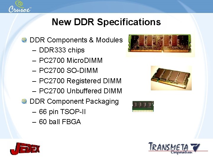
New DDR Specifications DDR Components & Modules – DDR 333 chips – PC 2700 Micro. DIMM – PC 2700 SO-DIMM – PC 2700 Registered DIMM – PC 2700 Unbuffered DIMM DDR Component Packaging – 66 pin TSOP-II – 60 ball FBGA Confidential and Proprietary Information
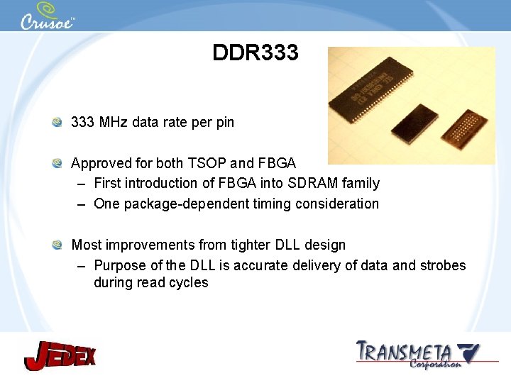
DDR 333 MHz data rate per pin Approved for both TSOP and FBGA – First introduction of FBGA into SDRAM family – One package-dependent timing consideration Most improvements from tighter DLL design – Purpose of the DLL is accurate delivery of data and strobes during read cycles Confidential and Proprietary Information

Achieving 333 Mbps Data Rate Confidential and Proprietary Information
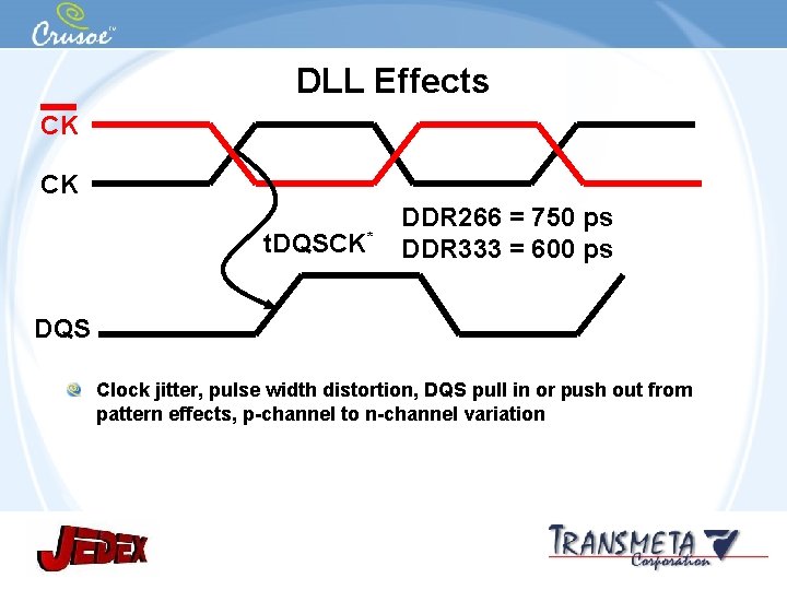
DLL Effects CK CK t. DQSCK* DDR 266 = 750 ps DDR 333 = 600 ps DQS Clock jitter, pulse width distortion, DQS pull in or push out from pattern effects, p-channel to n-channel variation Confidential and Proprietary Information
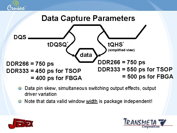
Data Capture Parameters DQS t. DQSQ* t. QHS* data DDR 266 = 750 ps DDR 333 = 450 ps for TSOP = 400 ps for FBGA (simplified view) DDR 266 = 750 ps DDR 333 = 550 ps for TSOP = 500 ps for FBGA Data pin skew, simultaneous switching output effects, output driver variation Note that data valid window width is package independent! Confidential and Proprietary Information
Managing Power Confidential and Proprietary Information
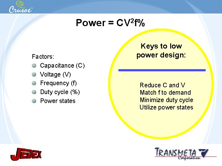
Power = CV 2 f% Factors: Capacitance (C) Voltage (V) Frequency (f) Duty cycle (%) Power states Keys to low power design: Reduce C and V Match f to demand Minimize duty cycle Utilize power states Confidential and Proprietary Information
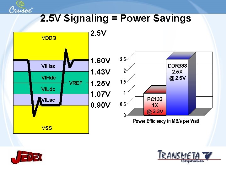
2. 5 V Signaling = Power Savings 2. 5 V VDDQ 1. 60 V 1. 43 V VIHac VIHdc VILac VREF 1. 25 V 1. 07 V 0. 90 V DDR 333 2. 5 X @ 2. 5 V PC 133 1 X @ 3. 3 V VSS Confidential and Proprietary Information
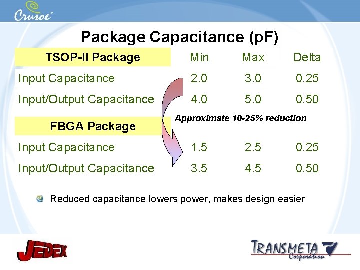
Package Capacitance (p. F) TSOP-II Package Min Max Delta Input Capacitance 2. 0 3. 0 0. 25 Input/Output Capacitance 4. 0 5. 0 0. 50 FBGA Package Approximate 10 -25% reduction Input Capacitance 1. 5 2. 5 0. 25 Input/Output Capacitance 3. 5 4. 5 0. 50 Reduced capacitance lowers power, makes design easier Confidential and Proprietary Information
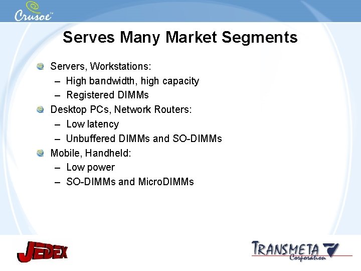
Serves Many Market Segments Servers, Workstations: – High bandwidth, high capacity – Registered DIMMs Desktop PCs, Network Routers: – Low latency – Unbuffered DIMMs and SO-DIMMs Mobile, Handheld: – Low power – SO-DIMMs and Micro. DIMMs Confidential and Proprietary Information
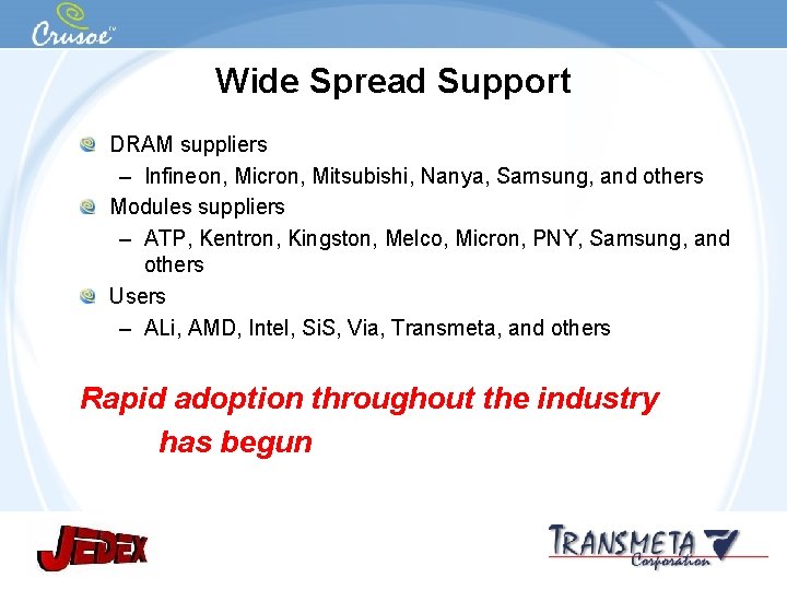
Wide Spread Support DRAM suppliers – Infineon, Micron, Mitsubishi, Nanya, Samsung, and others Modules suppliers – ATP, Kentron, Kingston, Melco, Micron, PNY, Samsung, and others Users – ALi, AMD, Intel, Si. S, Via, Transmeta, and others Rapid adoption throughout the industry has begun Confidential and Proprietary Information
Memory of choice for the future Simple transition from DDR 266 Widespread adoption in all market segments Confidential and Proprietary Information

Thank You Confidential and Proprietary Information
- Slides: 16