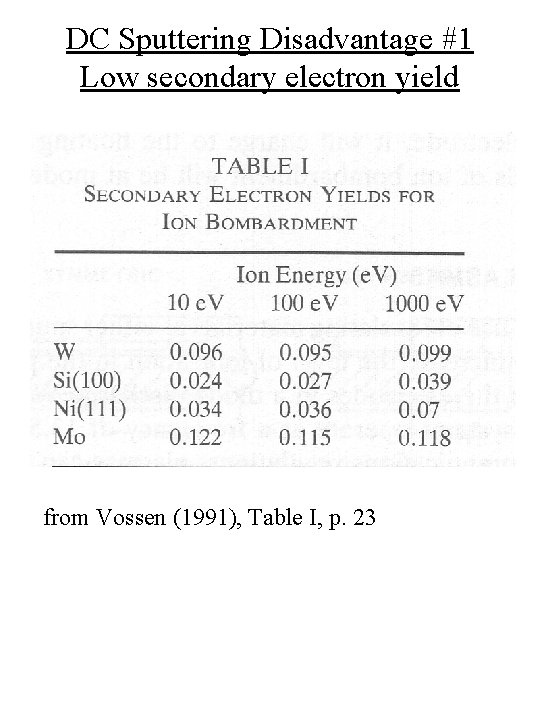
DC Sputtering Disadvantage 1 Low secondary electron yield
- Slides: 33

DC Sputtering Disadvantage #1 Low secondary electron yield from Vossen (1991), Table I, p. 23

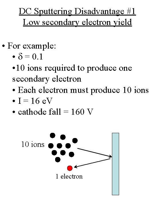
DC Sputtering Disadvantage #1 Low secondary electron yield • For example: • d = 0. 1 • 10 ions required to produce one secondary electron • Each electron must produce 10 ions • I = 16 e. V • cathode fall = 160 V 10 ions 1 electron

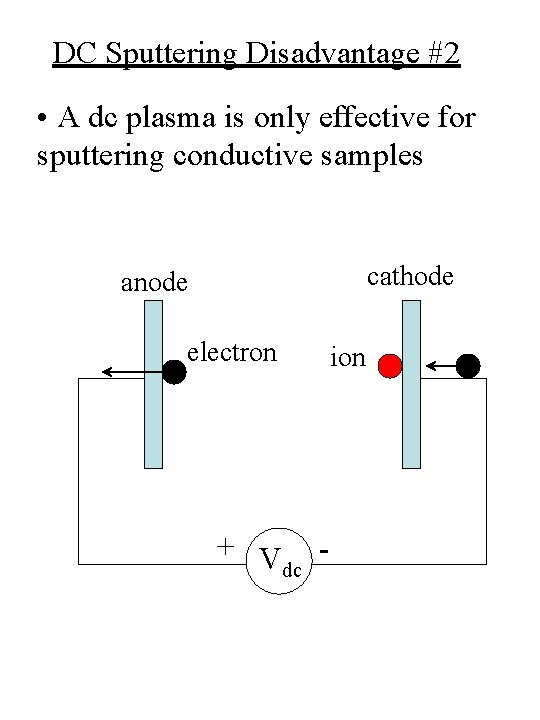
DC Sputtering Disadvantage #2 • A dc plasma is only effective for sputtering conductive samples cathode anode electron + V dc ion

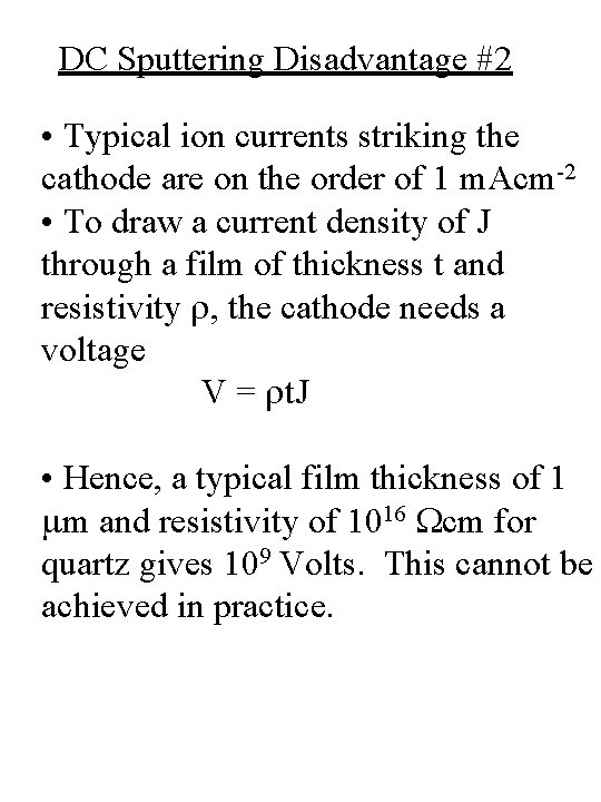
DC Sputtering Disadvantage #2 • Typical ion currents striking the cathode are on the order of 1 m. Acm-2 • To draw a current density of J through a film of thickness t and resistivity r, the cathode needs a voltage V = rt. J • Hence, a typical film thickness of 1 mm and resistivity of 1016 Wcm for quartz gives 109 Volts. This cannot be achieved in practice.

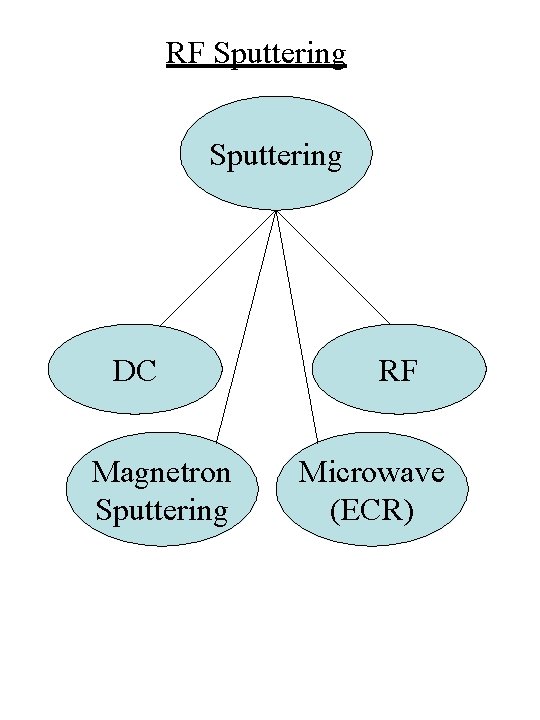
RF Sputtering DC Magnetron Sputtering RF Microwave (ECR)

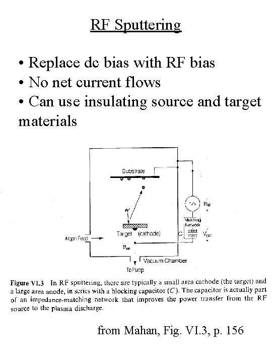
RF Sputtering • Replace dc bias with RF bias • No net current flows • Can use insulating source and target materials from Mahan, Fig. VI. 3, p. 156

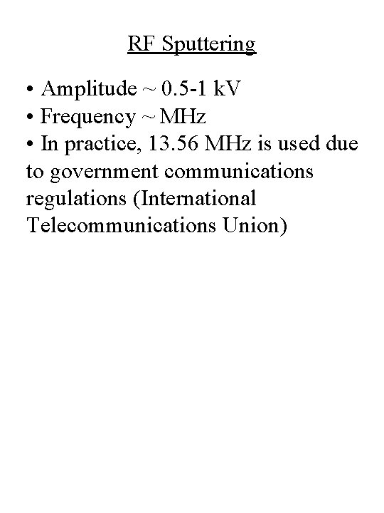
RF Sputtering • Amplitude ~ 0. 5 -1 k. V • Frequency ~ MHz • In practice, 13. 56 MHz is used due to government communications regulations (International Telecommunications Union)

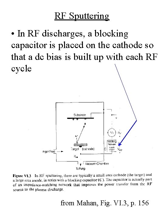
RF Sputtering • In RF discharges, a blocking capacitor is placed on the cathode so that a dc bias is built up with each RF cycle from Mahan, Fig. VI. 3, p. 156

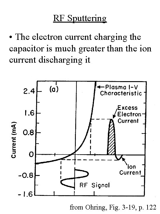
RF Sputtering Current (m. A) • The electron current charging the capacitor is much greater than the ion current discharging it from Ohring, Fig. 3 -19, p. 122

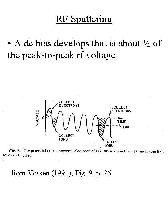
RF Sputtering • A dc bias develops that is about ½ of the peak-to-peak rf voltage from Vossen (1991), Fig. 9, p. 26

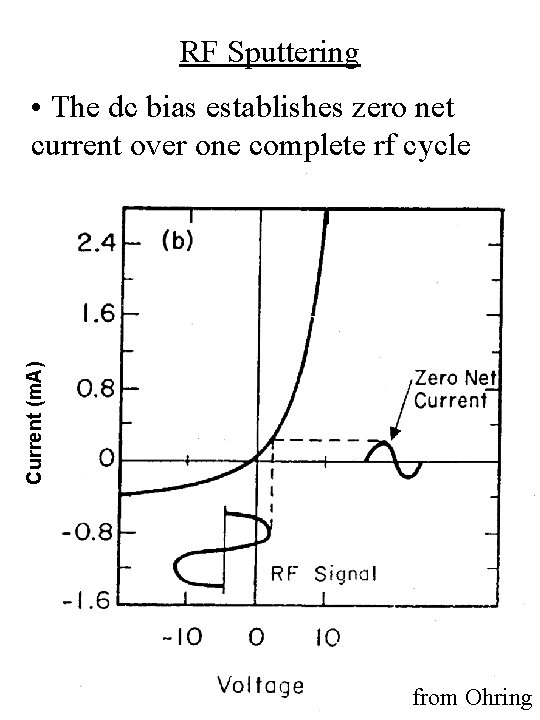
RF Sputtering Current (m. A) • The dc bias establishes zero net current over one complete rf cycle from Ohring

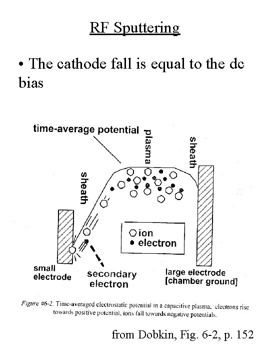
RF Sputtering • The cathode fall is equal to the dc bias from Dobkin, Fig. 6 -2, p. 152

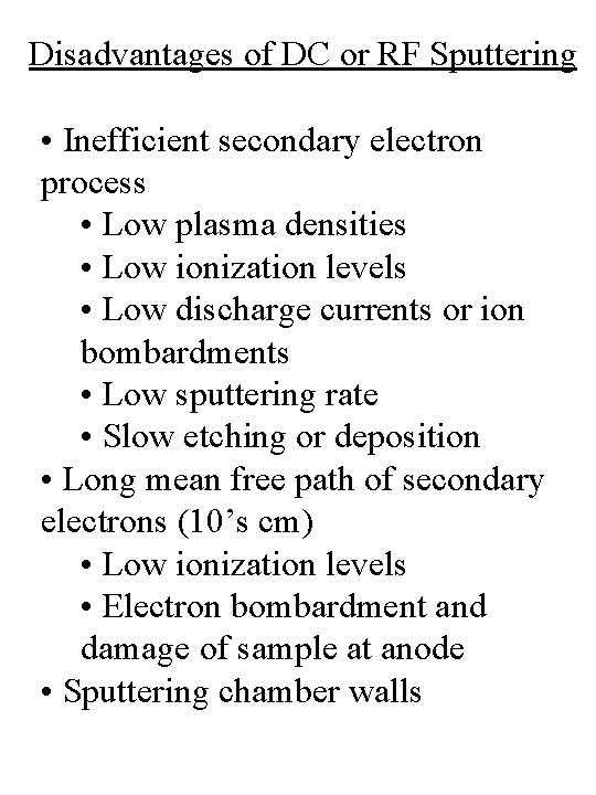
Disadvantages of DC or RF Sputtering • Inefficient secondary electron process • Low plasma densities • Low ionization levels • Low discharge currents or ion bombardments • Low sputtering rate • Slow etching or deposition • Long mean free path of secondary electrons (10’s cm) • Low ionization levels • Electron bombardment and damage of sample at anode • Sputtering chamber walls

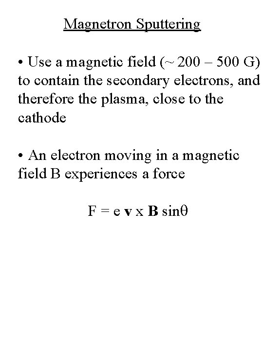
Magnetron Sputtering • Use a magnetic field (~ 200 – 500 G) to contain the secondary electrons, and therefore the plasma, close to the cathode • An electron moving in a magnetic field B experiences a force F = e v x B sinq

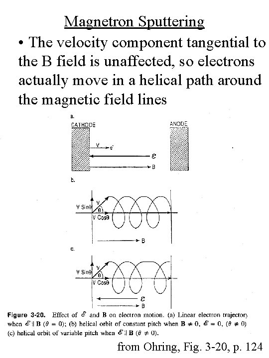
Magnetron Sputtering • The velocity component tangential to the B field is unaffected, so electrons actually move in a helical path around the magnetic field lines from Ohring, Fig. 3 -20, p. 124

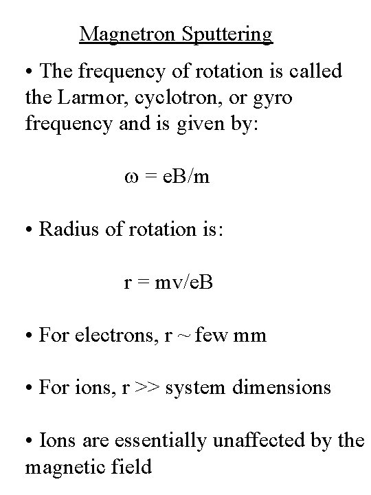
Magnetron Sputtering • The frequency of rotation is called the Larmor, cyclotron, or gyro frequency and is given by: w = e. B/m • Radius of rotation is: r = mv/e. B • For electrons, r ~ few mm • For ions, r >> system dimensions • Ions are essentially unaffected by the magnetic field

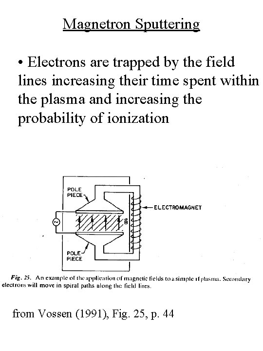
Magnetron Sputtering • Electrons are trapped by the field lines increasing their time spent within the plasma and increasing the probability of ionization from Vossen (1991), Fig. 25, p. 44

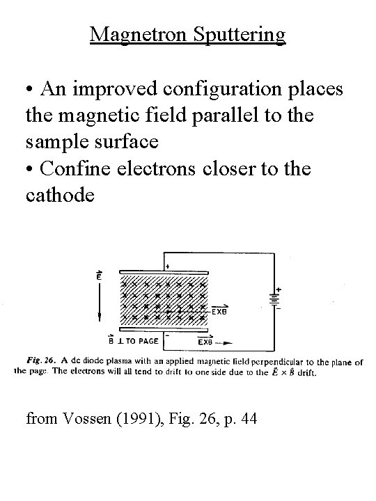
Magnetron Sputtering • An improved configuration places the magnetic field parallel to the sample surface • Confine electrons closer to the cathode from Vossen (1991), Fig. 26, p. 44

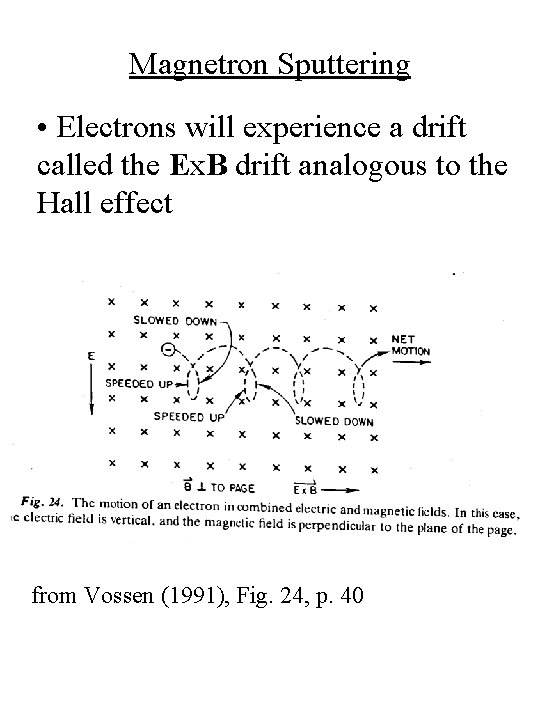
Magnetron Sputtering • Electrons will experience a drift called the Ex. B drift analogous to the Hall effect from Vossen (1991), Fig. 24, p. 40

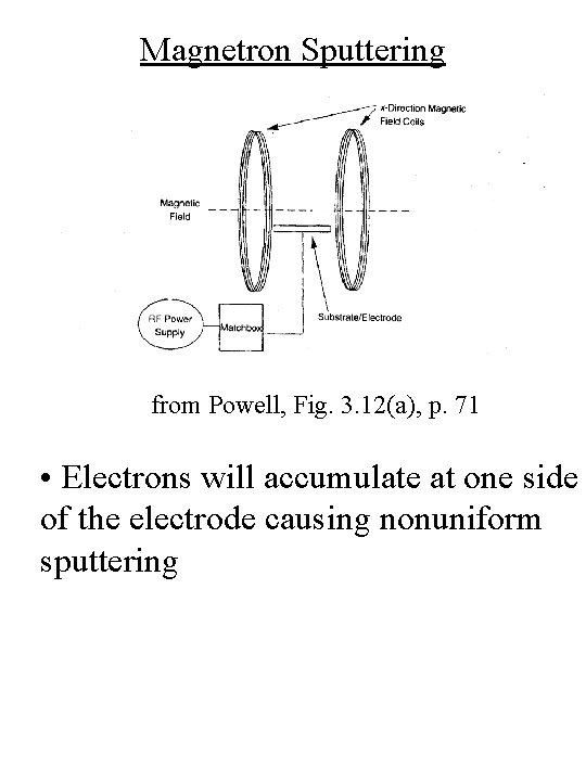
Magnetron Sputtering from Powell, Fig. 3. 12(a), p. 71 • Electrons will accumulate at one side of the electrode causing nonuniform sputtering

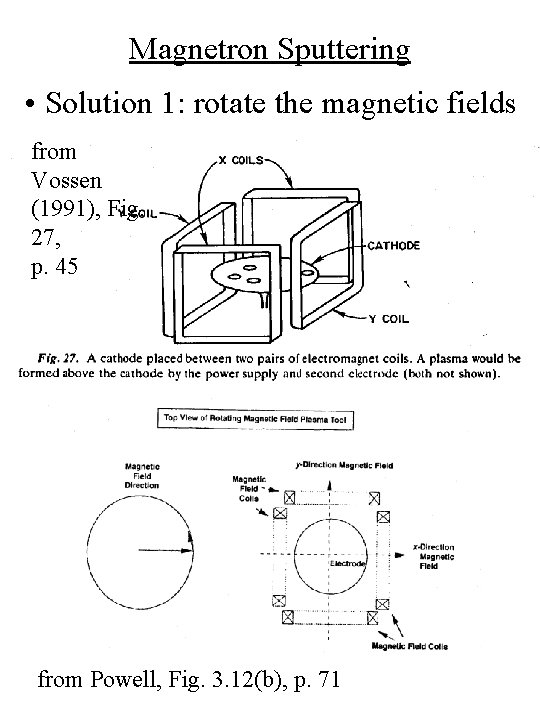
Magnetron Sputtering • Solution 1: rotate the magnetic fields from Vossen (1991), Fig. 27, p. 45 from Powell, Fig. 3. 12(b), p. 71

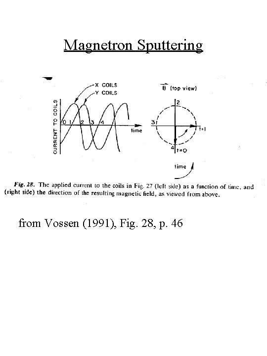
Magnetron Sputtering from Vossen (1991), Fig. 28, p. 46

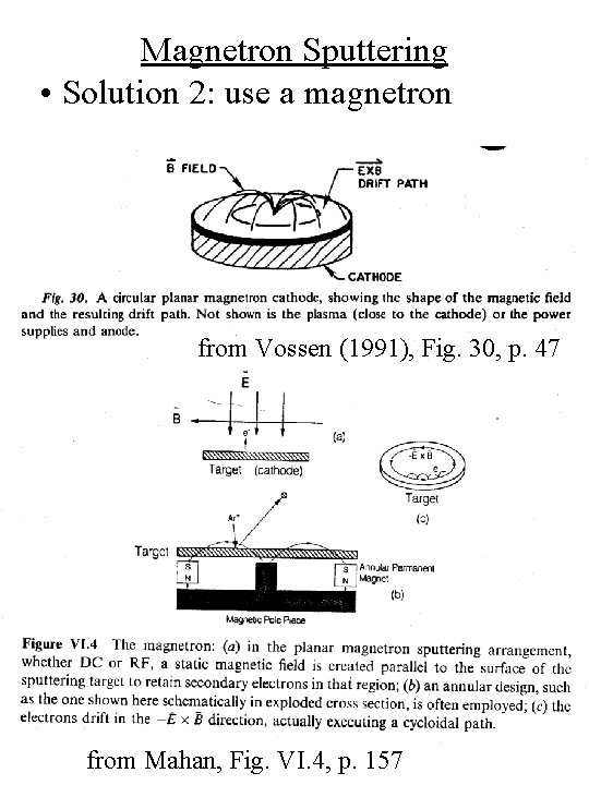
Magnetron Sputtering • Solution 2: use a magnetron from Vossen (1991), Fig. 30, p. 47 from Mahan, Fig. VI. 4, p. 157

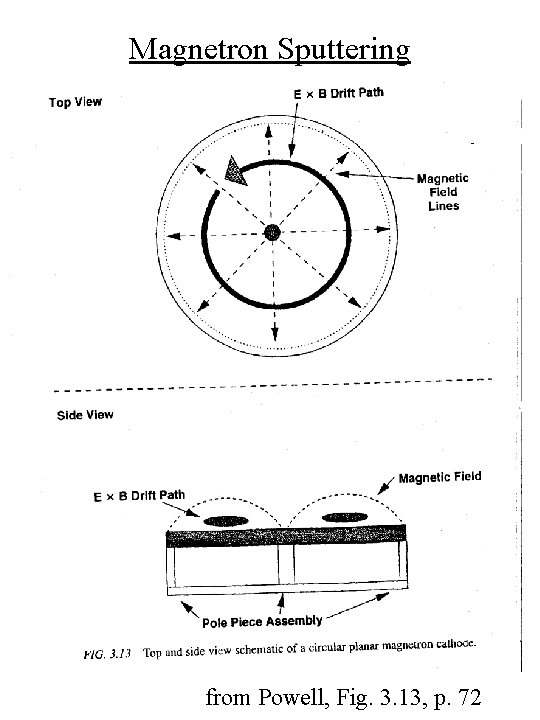
Magnetron Sputtering from Powell, Fig. 3. 13, p. 72

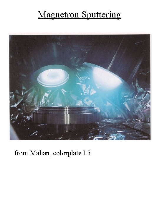
Magnetron Sputtering from Mahan, colorplate I. 5

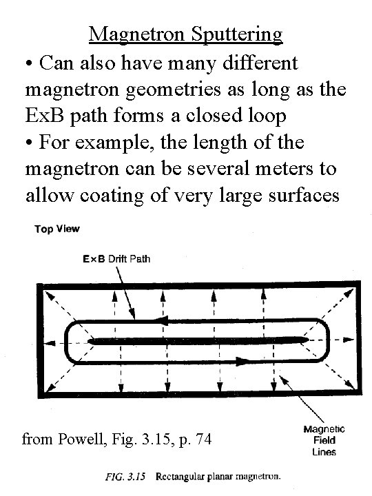
Magnetron Sputtering • Can also have many different magnetron geometries as long as the Ex. B path forms a closed loop • For example, the length of the magnetron can be several meters to allow coating of very large surfaces from Powell, Fig. 3. 15, p. 74

Magnetron Sputtering • Electrons are trapped for several trips around the Ex. B loops above the cathode (magnetic tunnel) • Increased ionization (ni/n ~ 10 -4 to 10 -2) • Higher plasma density (ni ~ 1011 cm-3) • Increased ion bombardment (4 -60 m. A/cm 2) • Higher deposition rates (~ 1 mm/min for Al) • Lower Ar pressures (0. 5 – 30 m. T) • Lower dc voltages (300 – 700 V) or RF voltages (< 500 V amplitude)

Sputtering Advantages • Can deposit refractory metals • High deposition rate • Sputtered particle energy ~ 3 -5 e. V >> evaporated particles • Higher surface mobility in condensing particles • Smooth and conformal film morphologies • Sputtering sources are typically of relatively large area • Can sputter alloys

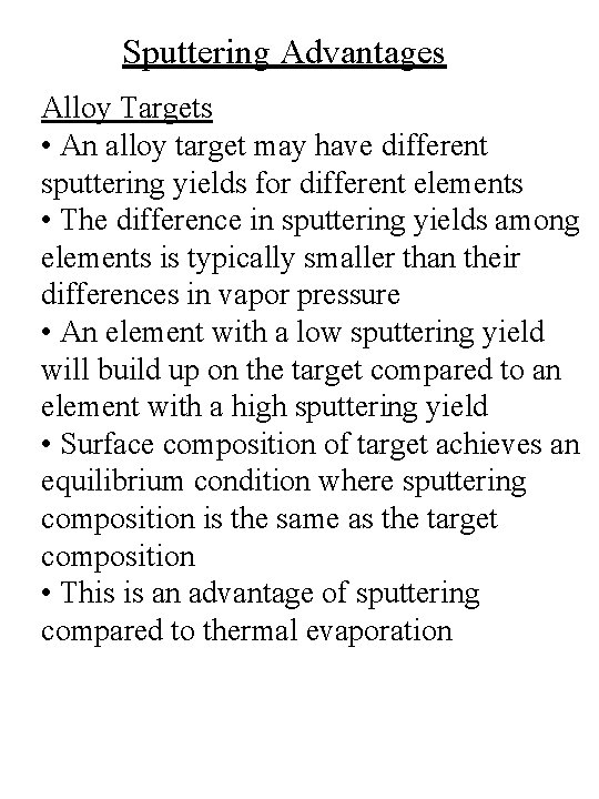
Sputtering Advantages Alloy Targets • An alloy target may have different sputtering yields for different elements • The difference in sputtering yields among elements is typically smaller than their differences in vapor pressure • An element with a low sputtering yield will build up on the target compared to an element with a high sputtering yield • Surface composition of target achieves an equilibrium condition where sputtering composition is the same as the target composition • This is an advantage of sputtering compared to thermal evaporation

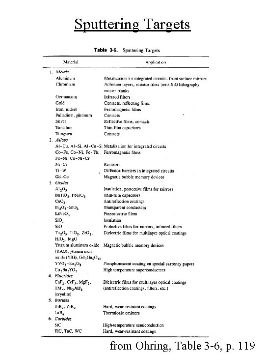
Sputtering Targets from Ohring, Table 3 -6, p. 119

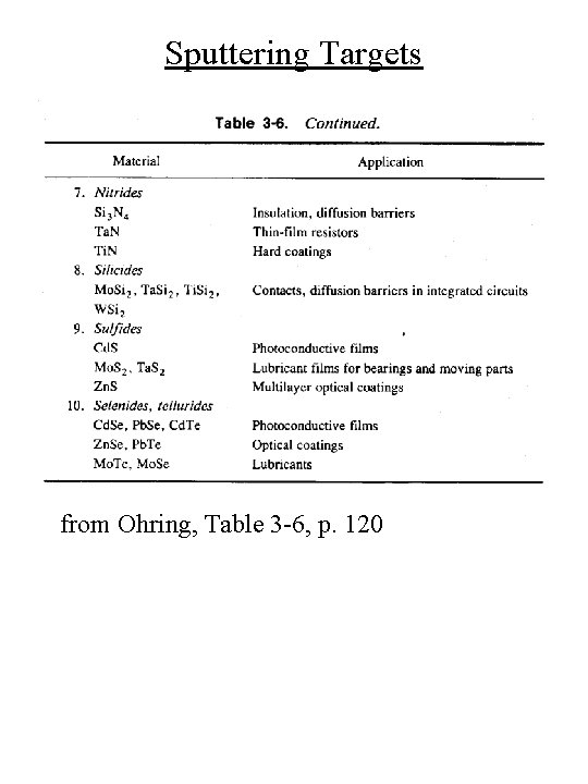
Sputtering Targets from Ohring, Table 3 -6, p. 120

Evaporation versus Sputtering from Ohring, Table 3 -7, p. 132

PVD Summary • Solid or molten sources • Source atoms enter the gas phase by physical mechanisms (evaporation or sputtering) • Gaseous source particles are transported through a reduced pressure environment • Generally, an absence of chemical reactions in the gas phase and at the substrate surface