DC and Parametric Tests Continuity Purpose of Continuity
- Slides: 45

DC and Parametric Tests

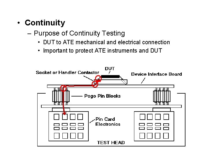
• Continuity – Purpose of Continuity Testing • DUT to ATE mechanical and electrical connection • Important to protect ATE instruments and DUT

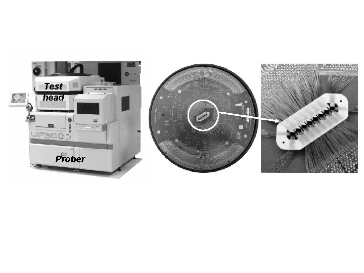
Test head Prober

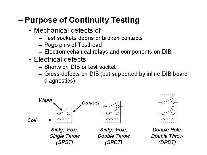
– Purpose of Continuity Testing • Mechanical defects of – Test sockets debris or broken contacts – Pogo pins of Testhead – Electromechanical relays and components on DIB • Electrical defects – Shorts on DIB or test socket – Gross defects on DIB (but supported by inline DIB board diagnostics) Wiper Contact Coil Sinlge Pole, Single Throw (SPST) Sinlge Pole, Double Throw (SPDT) Double Pole, Double Throw (DPDT)

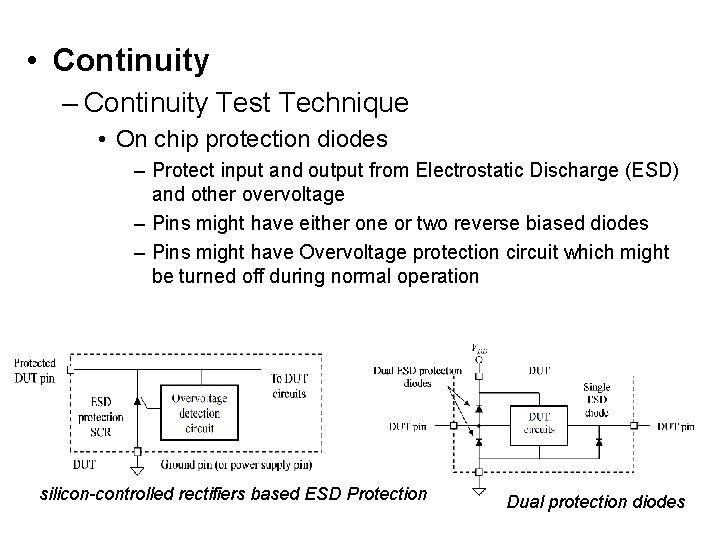
• Continuity – Continuity Test Technique • On chip protection diodes – Protect input and output from Electrostatic Discharge (ESD) and other overvoltage – Pins might have either one or two reverse biased diodes – Pins might have Overvoltage protection circuit which might be turned off during normal operation silicon-controlled rectifiers based ESD Protection Dual protection diodes

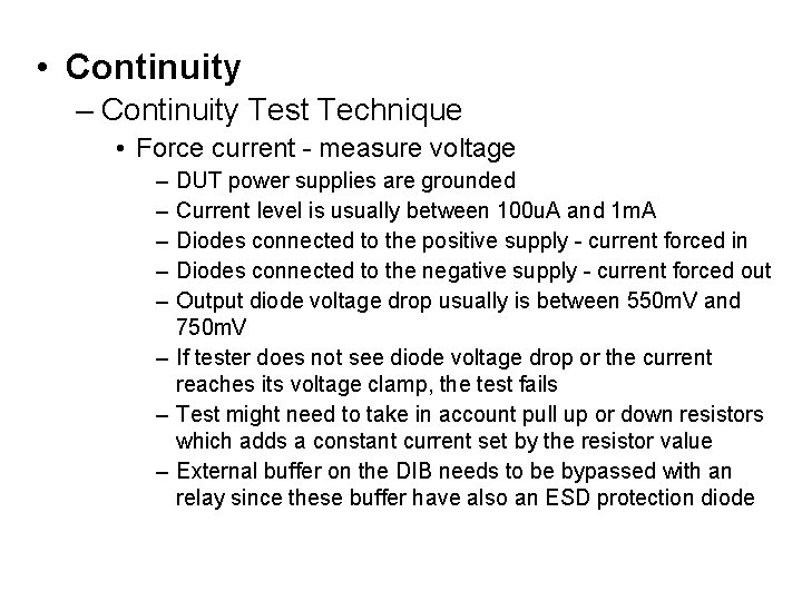
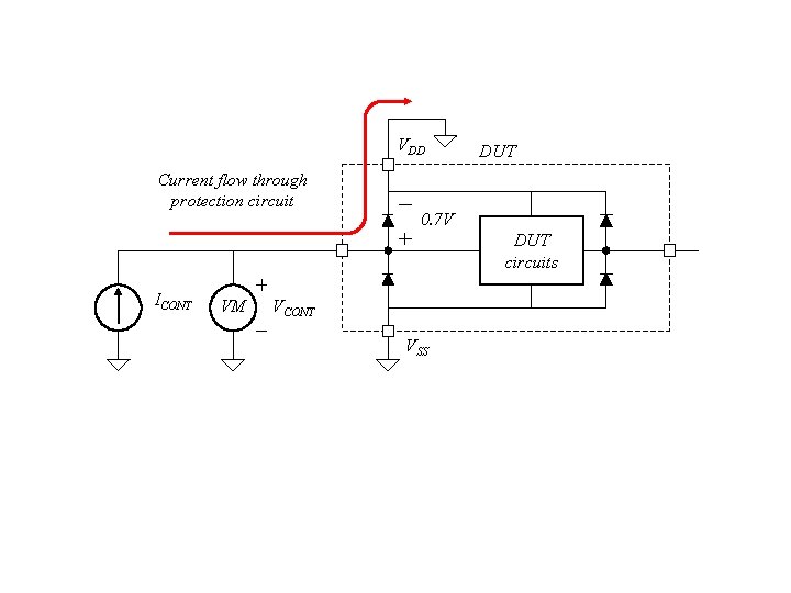
• Continuity – Continuity Test Technique • Force current - measure voltage – – – DUT power supplies are grounded Current level is usually between 100 u. A and 1 m. A Diodes connected to the positive supply - current forced in Diodes connected to the negative supply - current forced out Output diode voltage drop usually is between 550 m. V and 750 m. V – If tester does not see diode voltage drop or the current reaches its voltage clamp, the test fails – Test might need to take in account pull up or down resistors which adds a constant current set by the resistor value – External buffer on the DIB needs to be bypassed with an relay since these buffer have also an ESD protection diode

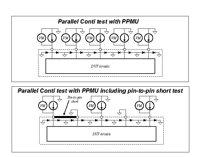
• Continuity – Serial vs. Parallel Continuity Testing • Serial is one pin at a time – Test time intensive • Parallel can not see pin to pin shorts – Alternating odd and even pin parallel test – Will need a PPMU (per pin measurement unit) • Analog parallel per-pin measurement is not available in some testers – Single current source and volt meter can be used one pin at a time • Digital per-pin measurement is available, but may introduce noise into sensitive analog circuit

VDD Current flow through protection circuit DUT 0. 7 V DUT circuits ICONT VM VCONT VSS

Parallel Conti test with PPMU VM VM VM DUT circuits Parallel Conti test with PPMU including pin-to-pin short test Pin-to-pin short VM VM DUT circuits VM

• Leakage Currents – Purpose of Leakage Testing • Good design should have leakage current of less than 1 u. A • First indication of poorly processed or damaged DUT – Improperation in manufacturing and handling including test – Improperation in customer end application • Detect weak devices – Initially function but eventually fail after unacceptably short lifetime (Infant mortality)

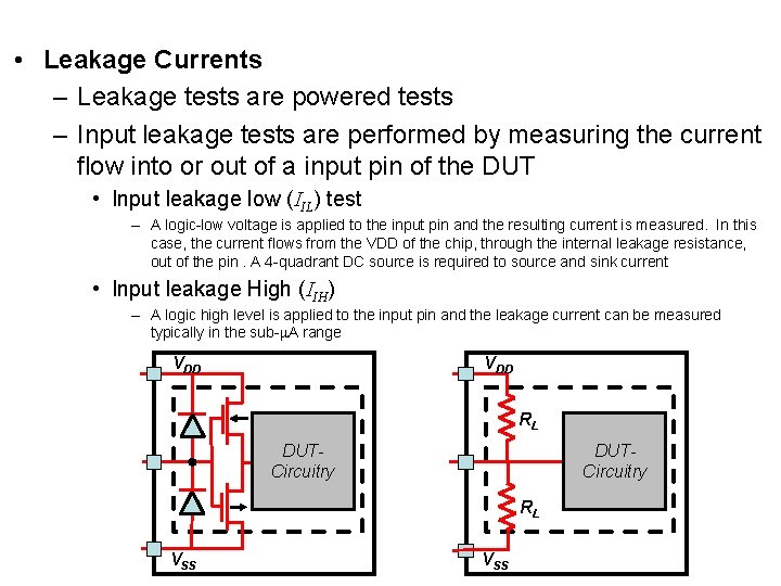
• Leakage Currents – Leakage tests are powered tests – Input leakage tests are performed by measuring the current flow into or out of a input pin of the DUT • Input leakage low (IIL) test – A logic-low voltage is applied to the input pin and the resulting current is measured. In this case, the current flows from the VDD of the chip, through the internal leakage resistance, out of the pin. A 4 -quadrant DC source is required to source and sink current • Input leakage High (IIH) – A logic high level is applied to the input pin and the leakage current can be measured typically in the sub-m. A range VDD RL DUTCircuitry RL VSS

• Leakage Currents – Leakage Test Technique • Output leakage current (IOZ) – Measured same as IIH & IIL » output pin must be placed in a high impedance (HIZ) state using test modes

• Leakage Currents – Serial vs. Parallel Leakage Testing • Serial is one pin at a time – Test time intensive – Less possibility of errors • Leakage currents can flow from pin to pin – Alternating odd and even pin parallel test is recommended • Analog parallel per-pin measurement is not available in some testers – Single voltage source and current meter can be used one pin at a time • Again, digital per-pin measurement is available, but may introduce noise into sensitive analog circuit

• Power Supply Currents – Importance of Supply Current Tests • Fast method for determining catastrophic failure – Large current draw from power supplies – Tests are run early in test protocol • Customer specific application characteristic – Battery operated instruments like a cellular phone require minimal current draw by electronics – Can often be used to correlate RF/AC performance parameter

• Power Supply Currents – Test Techniques • Basic test is simple – Testers have the ability to measure current draw from power supplies (Idd and Icc) • Actual test is never basic – Test conditions » must be clearly identified in test plan » power up mode, standby mode, normal operational mode » digital supply and analog measured separately » Load condition needs to be defined and settled » LDO, CP etc. needs to be in static mode

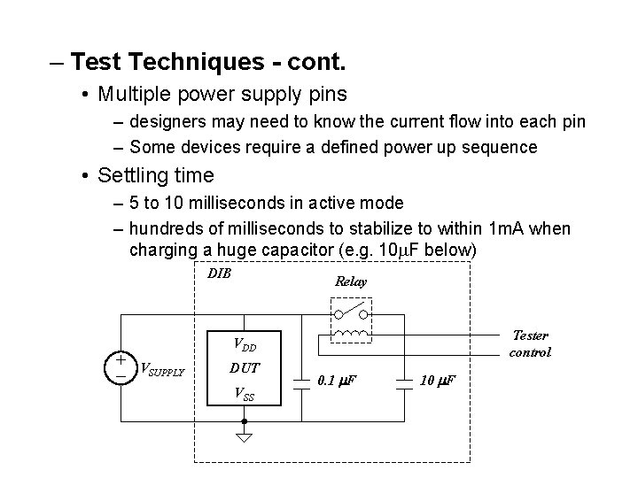
– Test Techniques - cont. • Multiple power supply pins – designers may need to know the current flow into each pin – Some devices require a defined power up sequence • Settling time – 5 to 10 milliseconds in active mode – hundreds of milliseconds to stabilize to within 1 m. A when charging a huge capacitor (e. g. 10 m. F below) DIB Relay Tester control VDD VSUPPLY DUT VSS 0. 1 F 10 F

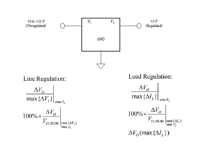
• DC References and Regulators – Voltage Regulators • High voltage input - regulated lower voltage output – Output voltage » simple voltmeter reading – Output voltage regulation » ability of regulator to maintain specific output under load – Dropout voltage » minimum input voltage before output drops below specified level – Input regulation » ability of regulator to maintain steady output with a range of input voltages

+6 to +12 V (Unregulated) VI Vo GND +5 V (Regulated)

• DC References and Regulators – Voltage References • Low power voltage regulators – Not always accessible from external pin » test engineer may need to request test modes to test references – May not have a separate specification in the data sheet – DC reference test modes allow the program to trim the DC references for more precise device operation

• DC References and Regulators – Trimmable References • Allows quality of product to be enhanced during testing through fuses or NVM (e. g. EEPROM) or OTP (one time programmable) links internal to the device – One aspect of testing that adds value to the device • Fuses, Zener diodes or EEPROM register bits – Fuses and Zener diodes are blown by forcing a controlled current through them » fuses blow to an open circuit » diodes blow to a short circuit • Trimming is sometimes performed after packaging to account for packaging effects

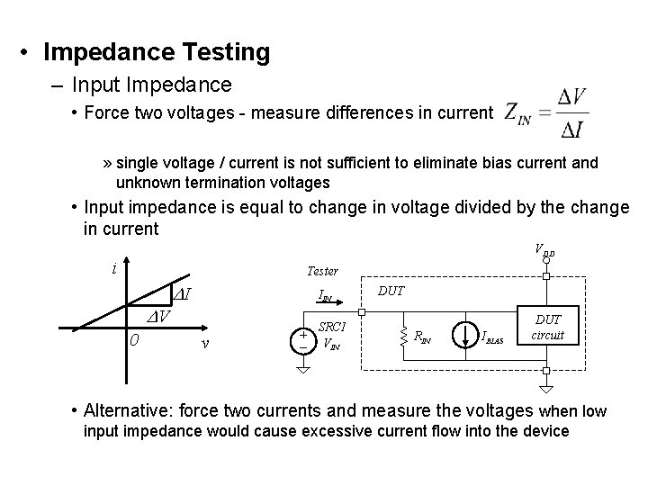
• Impedance Testing – Input Impedance • Force two voltages - measure differences in current » single voltage / current is not sufficient to eliminate bias current and unknown termination voltages • Input impedance is equal to change in voltage divided by the change in current VDD i Tester V 0 I IIN v SRC 1 VIN DUT RIN IBIAS DUT circuit • Alternative: force two currents and measure the voltages when low input impedance would cause excessive current flow into the device

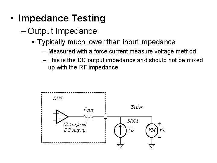
• Impedance Testing – Output Impedance • Typically much lower than input impedance – Measured with a force current measure voltage method – This is the DC output impedance and should not be mixed up with the RF impedance DUT ROUT (Set to fixed DC output) Tester SRC 1 IIN VM VO

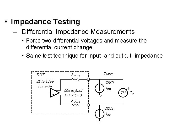
• Impedance Testing – Differential Impedance Measurements • Force two differential voltages and measure the differential current change • Same test technique for input- and output- impedance DUT ROUT 1 SE to DIFF converter (Set to fixed DC output) ROUT 2 Tester SRC 1 IIN 1 SRC 2 IIN 2 VM VO

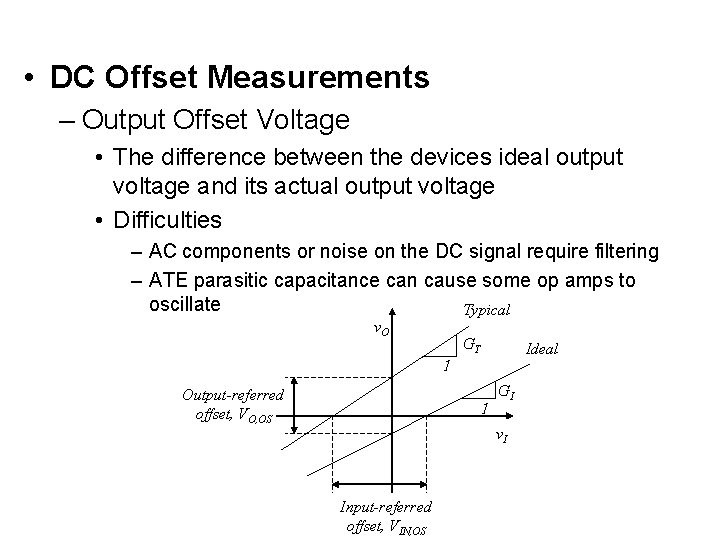
• DC Offset Measurements – Output Offset Voltage • The difference between the devices ideal output voltage and its actual output voltage • Difficulties – AC components or noise on the DC signal require filtering – ATE parasitic capacitance can cause some op amps to oscillate Typical v. O Output-referred offset, VO, OS GT Ideal GI v. I Input-referred offset, VIN, OS

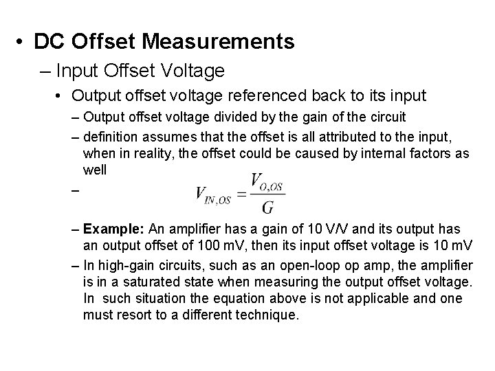
• DC Offset Measurements – Input Offset Voltage • Output offset voltage referenced back to its input – Output offset voltage divided by the gain of the circuit – definition assumes that the offset is all attributed to the input, when in reality, the offset could be caused by internal factors as well – – Example: An amplifier has a gain of 10 V/V and its output has an output offset of 100 m. V, then its input offset voltage is 10 m. V – In high-gain circuits, such as an open-loop op amp, the amplifier is in a saturated state when measuring the output offset voltage. In such situation the equation above is not applicable and one must resort to a different technique.

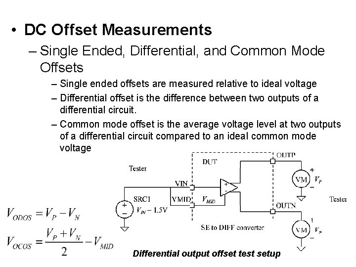
• DC Offset Measurements – Single Ended, Differential, and Common Mode Offsets – Single ended offsets are measured relative to ideal voltage – Differential offset is the difference between two outputs of a differential circuit. – Common mode offset is the average voltage level at two outputs of a differential circuit compared to an ideal common mode voltage Differential output offset test setup

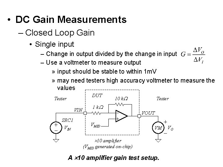
• DC Gain Measurements – Closed Loop Gain • Single input – Change in output divided by the change in input – Use a voltmeter to measure output » input should be stable to within 1 m. V » may need testers high accuracy voltmeter to measure the values DUT Tester VIN SRC 1 VIN 10 k Tester 1 k VOUT VMID VM 10 amplifier (VMID generated on-chip) A 10 amplifier gain test setup. VO

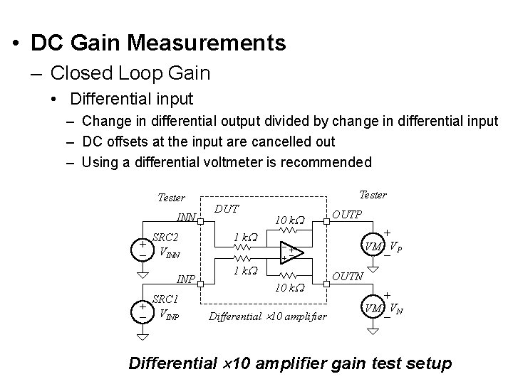
• DC Gain Measurements – Closed Loop Gain • Differential input – Change in differential output divided by change in differential input – DC offsets at the input are cancelled out – Using a differential voltmeter is recommended Tester INN SRC 2 VINN INP SRC 1 VINP Tester DUT 10 k OUTP 1 k VM VP 1 k 10 k Differential 10 amplifier OUTN VM VN Differential 10 amplifier gain test setup

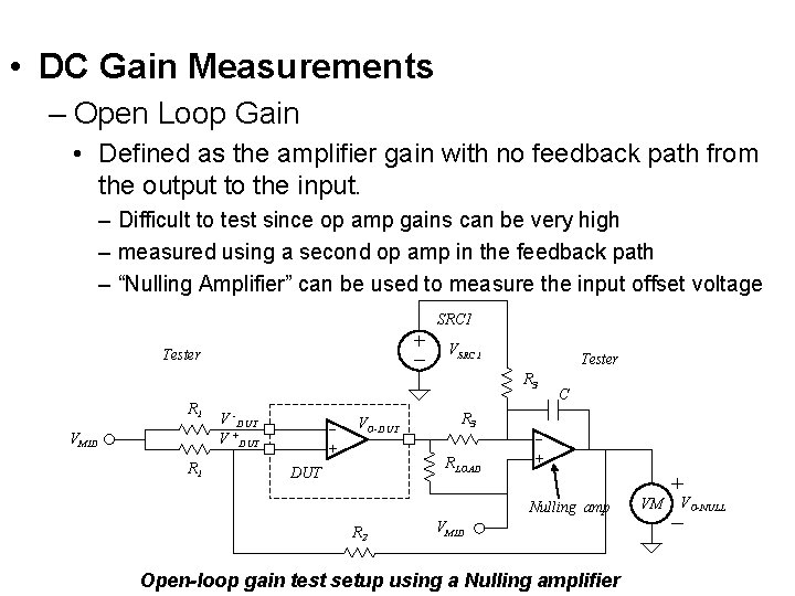
• DC Gain Measurements – Open Loop Gain • Defined as the amplifier gain with no feedback path from the output to the input. – Difficult to test since op amp gains can be very high – measured using a second op amp in the feedback path – “Nulling Amplifier” can be used to measure the input offset voltage SRC 1 VSRC 1 Tester R 3 R 1 VMID R 1 V -DUT V +DUT VO-DUT C R 3 RLOAD DUT Nulling amp R 2 VMID Open-loop gain test setup using a Nulling amplifier VM VO-NULL

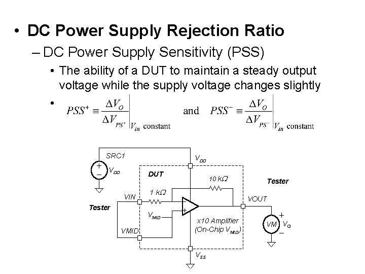
• DC Power Supply Rejection Ratio – DC Power Supply Sensitivity (PSS) • The ability of a DUT to maintain a steady output voltage while the supply voltage changes slightly • SRC 1 VDD DUT VIN Tester 1 k VMID 10 k Tester VOUT x 10 Amplifier (On-Chip VMID) VSS VM VO

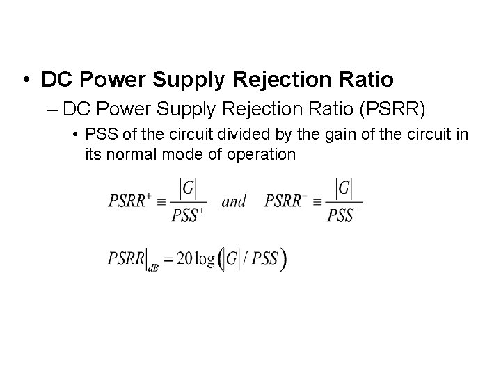
• DC Power Supply Rejection Ratio – DC Power Supply Rejection Ratio (PSRR) • PSS of the circuit divided by the gain of the circuit in its normal mode of operation

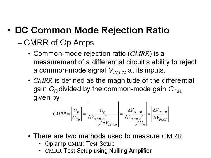
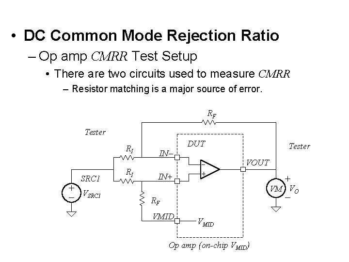
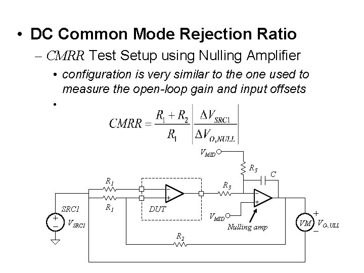
• DC Common Mode Rejection Ratio – CMRR of Op Amps • Common-mode rejection ratio (CMRR) is a measurement of a differential circuit’s ability to reject a common-mode signal VIN, CM at its inputs. • CMRR is defined as the magnitude of the differential gain GD divided by the common-mode gain GCM, given by • There are two methods used to measure CMRR • Op amp CMRR Test Setup • CMRR Test Setup using Nulling Amplifier

• DC Common Mode Rejection Ratio – Op amp CMRR Test Setup • There are two circuits used to measure CMRR – Resistor matching is a major source of error. RF Tester RI SRC 1 VSRC 1 RI IN DUT Tester VOUT IN+ VM VO RF VMID Op amp (on-chip VMID)

• DC Common Mode Rejection Ratio – CMRR Test Setup using Nulling Amplifier • configuration is very similar to the one used to measure the open-loop gain and input offsets • VMID R 3 R 1 SRC 1 R 1 C R 3 DUT VMID VSRC 1 R 2 Nulling amp VM VO-, ULL

• DC Common Mode Rejection Ratio – CMRR of Differential Gain Stages – Circuits that use op amps to perform a function – The CMRR of the op amp is not as critical as the CMRR of the circuit. – Resistor matching is critical in these circuits • Difference between chip CMRR and circuit CMRR? – Chip CMRR - the resistors are on the DIB. – Circuit CMRR - the resistors are on the DUT.

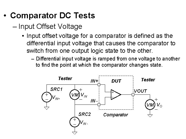
• Comparator DC Tests – Input Offset Voltage • Input offset voltage for a comparator is defined as the differential input voltage that causes the comparator to switch from one output logic state to the other. – Differential input voltage is ramped from one voltage to another to find the point at which the comparator changes state. Tester IN+ DUT SRC 1 VIN+ VM VIN VOUT IN SRC 2 VIN - Tester VM VO Comparator

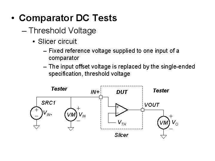
• Comparator DC Tests – Threshold Voltage • Slicer circuit – Fixed reference voltage supplied to one input of a comparator – The input offset voltage is replaced by the single-ended specification, threshold voltage Tester IN+ DUT SRC 1 VIN+ Tester VOUT VM VIN VTH Slicer VM VO

• Comparator DC Tests – Hysteresis • Hysteresis is defined as the difference in threshold voltage between a rising input test condition and a falling input condition • Input offset voltage and hysteresis may change with different common mode input voltages

• Voltage Search Techniques – Binary Searches vs. Step Searches • Ramping input voltages until an output condition is met is called a ramp or step search. – Very time consuming, not well suited for production testing. • Binary searches use successive approximation algorithms » If you are looking for a transition between 1. 45 V and 1. 55 V, the comparator input is set to 1. 5 V and the output is observed. If the output is high, then the input is increased by one quarter of the 100 m. V search range (25 m. V) to try to make the output go low. Once the output goes low, the input is adjusted by one eighth of the search range (12. 5 m. V) and the process is repeated until the desired resolution is attained. » Does not work well in the presence of hysteresis. » Measurement accuracy and resolution needs to be taken into account when setting the target

• Voltage Search Techniques – Linear Searches • Linear circuits can make use of an even faster search technique called a linear search • Linear search is similar to the binary search, except that the input approximations are based on a linear interpolation of input-output relationships – Using two input values, two output values can be measured. – Using the linear equation: y = m * x + b, the zero crossing values can be calculated. • Iterative linear searches are used to achieve the desired accuracy.

• DC Tests for Digital Circuits – IIH and IIL discussed earlier under leakage currents – The input high voltage (VIH) and input low voltage (VIL) specify the threshold voltage for digital inputs – VIH / VIL • Threshold voltage for digital inputs – Tested using a binary or step search – Force levels as a go/no-go test » to identify VIH / VIL threshold failures, rerunning the go/nogo test at a looser test limit will reveal the failure.

• DC Tests for Digital Circuits – VOH / VOL • VOH and VOL are the output equivalent of VIH and VIL • VOH is the minimum output voltage in the high state • VOL is the maximum output voltage in the low state – Usually a verified value not a measured value – Tested using a go/no-go test – IOH / IOL • VOH and VOL levels are guaranteed while the outputs are loaded with specified load currents, IOH and IOL. – When output is high, the tester must pull current out of the DUT. – When the output is low, the tester must force current into the DUT.

• DC Tests for Digital Circuits – IOSH and IOSL Short Circuit Current • Digital outputs often include a current-limiting feature that protects the output pins from damage during short circuit conditions • If the output is shorted directly to ground or to power, the amount of current flowing into or out of the pin is limited to IOSH and IOSL • Short circuit current is measured by setting the output to a low state and forcing a high voltage (usually VDD) into the pin

• Summary – DC tests are very easy to define and understand – Actual testing is usually much more difficult than it looks. • A DC offset of 100 m. V is easy to measure with an accuracy of +/- 10 m. V - very difficult to measure with an accuracy of 1 u. V. • Accuracy and repeatability are often the most time consuming problems faced by an analog test engineer. • For all DC measurements the DUT set-up needs to be clearly defined and setup per specification or test matrix

HW • • 3. 1~4; 3. 7~8; 3. 11~12; 3. 14; 3. 17; 3. 19; 3. 20~21; 3. 23~24;