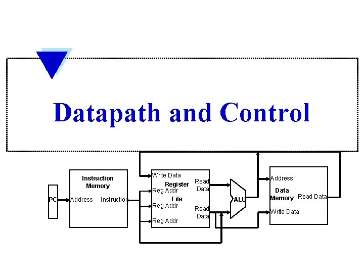
Datapath and Control Instruction Memory PC Address Instruction
![Datapath with Control Unit 0 Add ALUOp Instr[31 -26] Control Unit PC Read Address Datapath with Control Unit 0 Add ALUOp Instr[31 -26] Control Unit PC Read Address](https://slidetodoc.com/presentation_image_h2/40fd7d4a969e20056ceba8eb684a3af6/image-7.jpg)
![Adding Jump Operation Instr[25 -0] Shift left 2 26 28 1 32 0 PC+4[31 Adding Jump Operation Instr[25 -0] Shift left 2 26 28 1 32 0 PC+4[31](https://slidetodoc.com/presentation_image_h2/40fd7d4a969e20056ceba8eb684a3af6/image-12.jpg)
- Slides: 14

Datapath and Control Instruction Memory PC Address Instruction Write Data Read Register Data Reg Addr File Reg Addr Read Data Reg Address ALU Data Memory Read Data Write Data

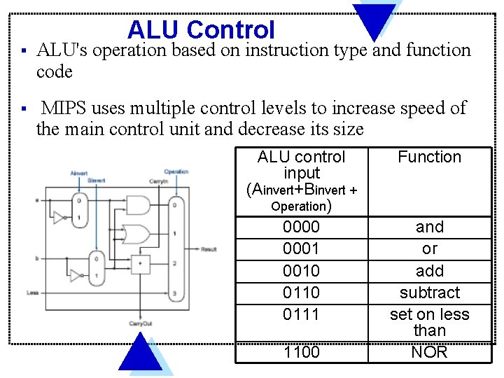
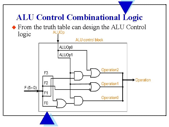
ALU Control § ALU's operation based on instruction type and function code § MIPS uses multiple control levels to increase speed of the main control unit and decrease its size ALU control input (Ainvert+Binvert + Operation) 0000 0001 0010 0111 1100 Function and or add subtract set on less than NOR

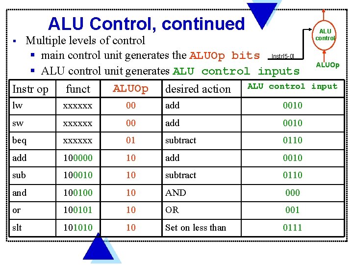
ALU Control, continued Multiple levels of control § main control unit generates the ALUOp bits Instr[5 -0] § ALU control unit generates ALU control inputs ALUOp desired action ALU control Instr op funct § lw xxxxxx 00 add 0010 sw xxxxxx 00 add 0010 beq xxxxxx 01 subtract 0110 add 100000 10 add 0010 sub 100010 10 subtract 0110 and 100100 10 AND 000 or 100101 10 OR 001 slt 101010 10 Set on less than 0111 ALU control ALUOp input

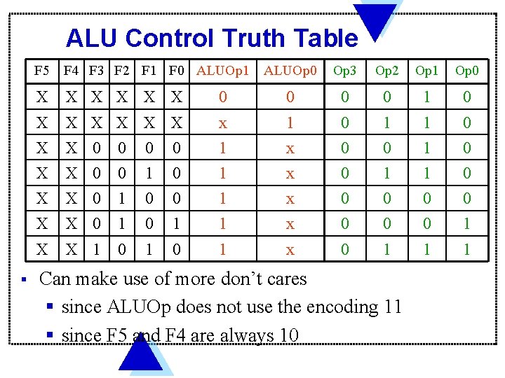
ALU Control Truth Table § F 5 F 4 F 3 F 2 F 1 F 0 ALUOp 1 ALUOp 0 Op 3 Op 2 Op 1 Op 0 X X X 0 0 1 0 X X X X 0 0 x 1 1 x 0 0 1 1 0 0 X X 0 0 1 x 0 1 1 0 X X X 0 1 1 0 0 0 1 1 1 x x 0 0 0 0 1 X X 1 0 1 x 0 1 1 1 Can make use of more don’t cares § since ALUOp does not use the encoding 11 § since F 5 and F 4 are always 10

ALU Control Combinational Logic u From logic the truth table can design the ALU Control

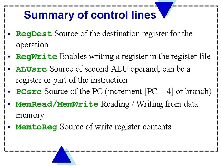
Summary of control lines § § § Reg. Dest Source of the destination register for the operation Reg. Write Enables writing a register in the register file ALUsrc Source of second ALU operand, can be a register or part of the instruction PCsrc Source of the PC (increment [PC + 4] or branch) Mem. Read/Mem. Write Reading / Writing from data memory Memto. Reg Source of write register contents
![Datapath with Control Unit 0 Add ALUOp Instr31 26 Control Unit PC Read Address Datapath with Control Unit 0 Add ALUOp Instr[31 -26] Control Unit PC Read Address](https://slidetodoc.com/presentation_image_h2/40fd7d4a969e20056ceba8eb684a3af6/image-7.jpg)
Datapath with Control Unit 0 Add ALUOp Instr[31 -26] Control Unit PC Read Address Instr[31 -0] Mem. Read Memto. Reg ALUSrc Mem. Write Reg. Write ovf Instr[25 -21] Read Addr 1 Read Register Instr[20 -16] Read Addr 2 Data 1 File 0 Write Addr Read 1 Instr[15 -11] Instr[15 -0] 1 PCSrc Branch Reg. Dst Instruction Memory Add Shift left 2 4 Write Data zero 0 ALU Data 2 1 Sign 16 Extend 32 Instr[5 -0] ALU control Address Data Memory Read Data 1 Write Data 0

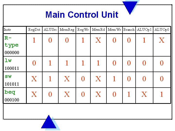
Main Control Unit Instr Rtype Reg. Dst ALUSrc Mem. Reg. Wr Mem. Rd Mem. Wr Branch ALUOp 1 ALUOp 0 1 0 0 1 X 0 1 1 0 0 X 1 X 0 X 1 0 0 0 X 0 X 0 1 X 1 000000 lw 100011 sw 101011 beq 000100

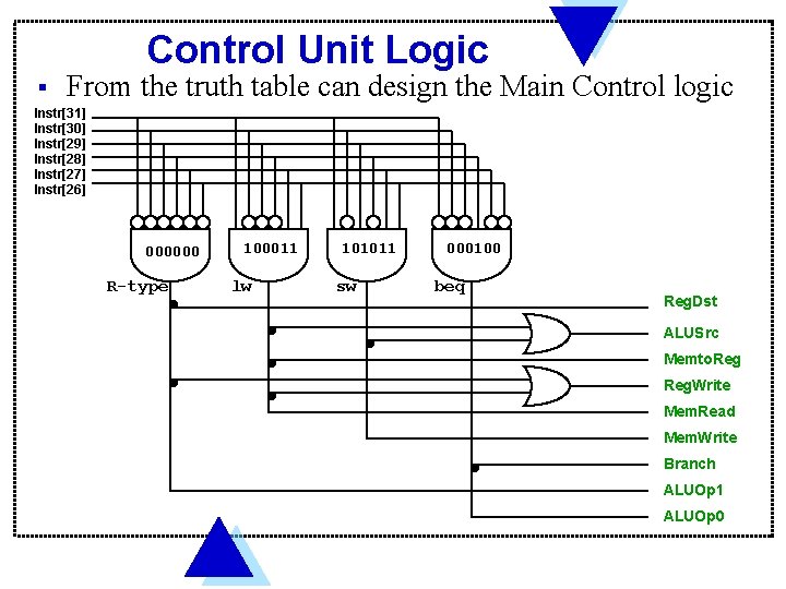
Control Unit Logic § From the truth table can design the Main Control logic Instr[31] Instr[30] Instr[29] Instr[28] Instr[27] Instr[26] 000000 R-type 100011 lw 101011 sw 000100 beq Reg. Dst ALUSrc Memto. Reg. Write Mem. Read Mem. Write Branch ALUOp 1 ALUOp 0

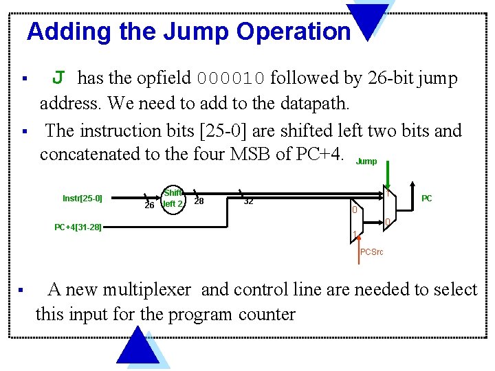
Adding the Jump Operation § J has the opfield 000010 followed by 26 -bit jump § address. We need to add to the datapath. The instruction bits [25 -0] are shifted left two bits and concatenated to the four MSB of PC+4. Jump Instr[25 -0] PC+4[31 -28] 26 Shift left 2 28 32 1 PC 0 0 1 PCSrc § A new multiplexer and control line are needed to select this input for the program counter

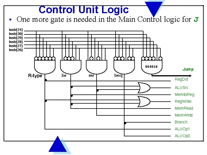
Control Unit Logic § One more gate is needed in the Main Control logic for J Instr[31] Instr[30] Instr[29] Instr[28] Instr[27] Instr[26] 000010 R-type lw sw beq Jump Reg. Dst ALUSrc Memto. Reg. Write Mem. Read Mem. Write Branch ALUOp 1 ALUOp 0
![Adding Jump Operation Instr25 0 Shift left 2 26 28 1 32 0 PC431 Adding Jump Operation Instr[25 -0] Shift left 2 26 28 1 32 0 PC+4[31](https://slidetodoc.com/presentation_image_h2/40fd7d4a969e20056ceba8eb684a3af6/image-12.jpg)
Adding Jump Operation Instr[25 -0] Shift left 2 26 28 1 32 0 PC+4[31 -28] 0 Add ALUOp Branch Instr[31 -26] Control Unit Reg. Dst Instruction Memory PC Read Address Instr[31 -0] Jump PCSrc ALUSrc Reg. Write ovf 1 Instr[15 -0] 1 Mem. Read Memto. Reg Mem. Write Instr[25 -21] Read Addr 1 Register Read Instr[20 -16] Read Addr 2 Data 1 File 0 Write Addr Read Instr[15 -11] Add Shift left 2 4 Write Data zero 0 ALU Data 2 1 Sign 16 Extend 32 Instr[5 -0] ALU control Address Data Memory Read Data 1 Write Data 0

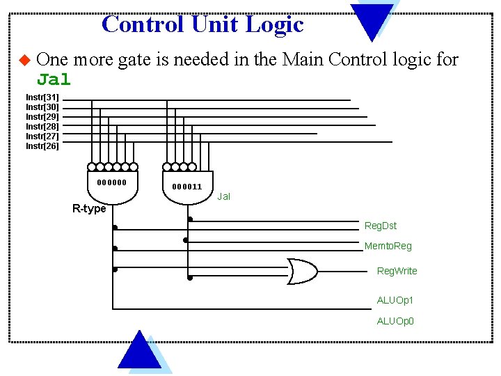
Control Unit Logic u One Jal more gate is needed in the Main Control logic for Instr[31] Instr[30] Instr[29] Instr[28] Instr[27] Instr[26] 00000011 Jal R-type Reg. Dst Memto. Reg. Write ALUOp 1 ALUOp 0

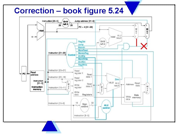
Correction – book figure 5. 24