Data Concentrator Card and Test System for the
![FE Interface Event Memories 6 SRAM [ 8 Mbit] 12 x 16 bits 12 FE Interface Event Memories 6 SRAM [ 8 Mbit] 12 x 16 bits 12](https://slidetodoc.com/presentation_image/d7a0445527ede8b83185c7fa71cc2e25/image-9.jpg)
- Slides: 17

Data Concentrator Card and Test System for the CMS ECAL Readout Presentation Outline ØECAL OD Electronics and Readout Architecture ØDCC System ØDCC TC System ØTest Bench LECC Amsterdam 29 Sept-3 Oct, 2003 - Nuno Almeida 1

DCC Team Project Manager João Varela DCC and DCC-TC Design and Conception José C. Da Silva, Nuno Cardoso Data Simulation, Control and Monitoring Software Nuno Almeida, Reyes Alemany LECC Amsterdam 29 Sept-3 Oct, 2003 - Nuno Almeida 2

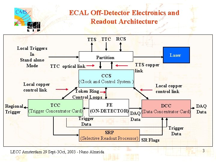
ECAL Off-Detector Electronics and Readout Architecture TTS Local Triggers In Stand alone Mode TTC optical link Local copper control link Regional Trigger TTC RCS Laser Partition CCS (Clock and Control System ) TTS copper link Token Ring Control Loops TCC (Trigger Concentrator Card) FE (ON-DETECTOR) Trigger Data Local copper control link DCC DAQ (Data Concentrator Card) Data SRP (Selective Readout Processor) SR Flags LECC Amsterdam 29 Sept-3 Oct, 2003 - Nuno Almeida DAQ Data Trigger Data 3

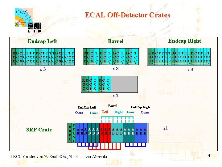
ECAL Off-Detector Crates Endcap Left Endcap Right Barrel R D C T T T TD C T T O C C CC C C C S C C C C RDC T OCC C CCS C R D C T T T TD C T T O C C CC C C C S C C C C x 8 x 3 RDC T OCC C CCS C x 2 Barrel End. Cap Left Outer SRP Crate Inner Left Right End. Cap Righ Inner Outer T S T A A A A A R C B B B B B P S C I LECC Amsterdam 29 Sept-3 Oct, 2003 - Nuno Almeida x 1 4

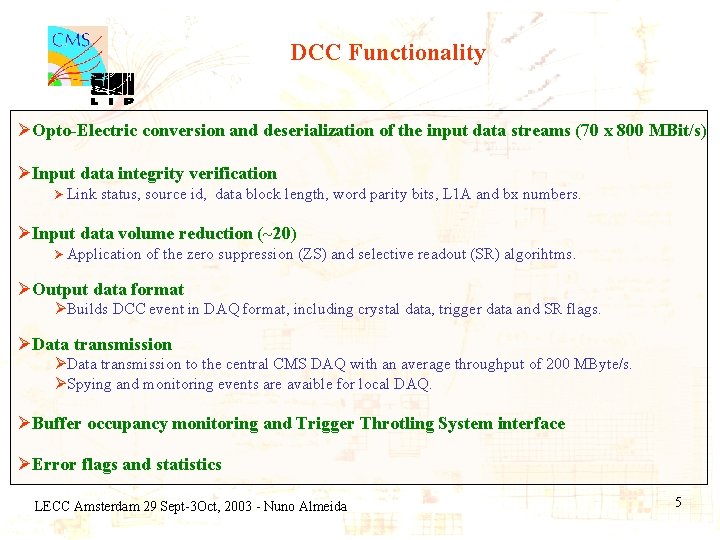
DCC Functionality ØOpto-Electric conversion and deserialization of the input data streams (70 x 800 MBit/s) ØInput data integrity verification Ø Link status, source id, data block length, word parity bits, L 1 A and bx numbers. ØInput data volume reduction (~20) Ø Application of the zero suppression (ZS) and selective readout (SR) algorihtms. ØOutput data format ØBuilds DCC event in DAQ format, including crystal data, trigger data and SR flags. ØData transmission to the central CMS DAQ with an average throughput of 200 MByte/s. ØSpying and monitoring events are avaible for local DAQ. ØBuffer occupancy monitoring and Trigger Throtling System interface ØError flags and statistics LECC Amsterdam 29 Sept-3 Oct, 2003 - Nuno Almeida 5

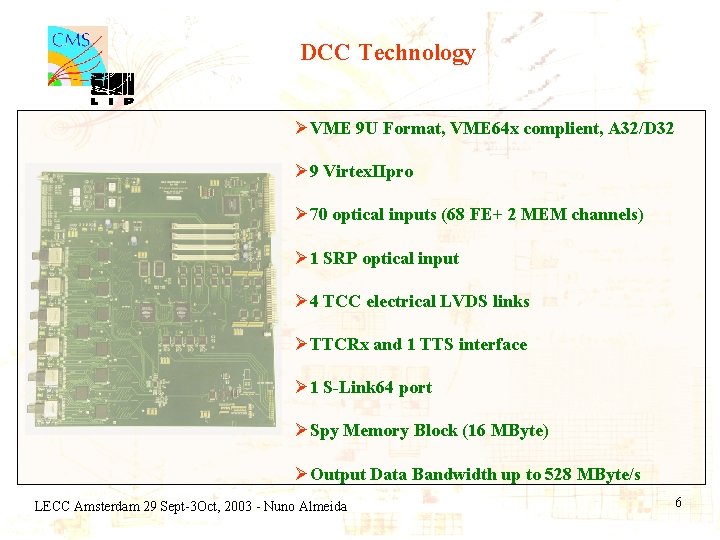
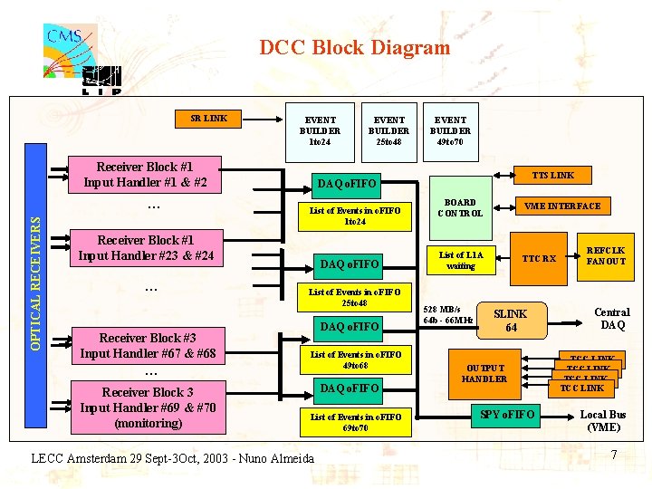
DCC Technology ØVME 9 U Format, VME 64 x complient, A 32/D 32 Ø 9 Virtex. IIpro Ø 70 optical inputs (68 FE+ 2 MEM channels) Ø 1 SRP optical input Ø 4 TCC electrical LVDS links ØTTCRx and 1 TTS interface Ø 1 S-Link 64 port ØSpy Memory Block (16 MByte) ØOutput Data Bandwidth up to 528 MByte/s LECC Amsterdam 29 Sept-3 Oct, 2003 - Nuno Almeida 6

DCC Block Diagram SR LINK EVENT BUILDER 1 to 24 Receiver Block #1 Input Handler #1 & #2 OPTICAL RECEIVERS … Receiver Block #3 Input Handler #67 & #68 … Receiver Block 3 Input Handler #69 & #70 (monitoring) EVENT BUILDER 49 to 70 TTS LINK DAQ o. FIFO List of Events in o. FIFO 1 to 24 Receiver Block #1 Input Handler #23 & #24 … EVENT BUILDER 25 to 48 DAQ o. FIFO List of Events in o. FIFO 49 to 68 DAQ o. FIFO List of Events in o. FIFO 69 to 70 LECC Amsterdam 29 Sept-3 Oct, 2003 - Nuno Almeida BOARD CONTROL VME INTERFACE List of L 1 A waiting TTC RX 528 MB/s 64 b - 66 MHz SLINK 64 OUTPUT HANDLER SPY o. FIFO REFCLK FANOUT Central DAQ TCC LINK Local Bus (VME) 7

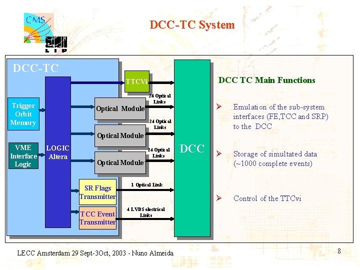
DCC-TC System DCC-TC DCC TC Main Functions TTCVi 24 Optical Links Trigger Orbit Memory Optical Module Ø Emulation of the sub-system interfaces (FE, TCC and SRP) to the DCC Ø Storage of simultated data (~1000 complete events) Ø Control of the TTCvi 24 Optical Links Optical Module VME Interface Logic LOGIC Altera 24 Optical Links DCC Optical Module SR Flags Transmitter TCC Event Transmitter 1 Optical Link 4 LVDS electrical Links LECC Amsterdam 29 Sept-3 Oct, 2003 - Nuno Almeida 8
![FE Interface Event Memories 6 SRAM 8 Mbit 12 x 16 bits 12 FE Interface Event Memories 6 SRAM [ 8 Mbit] 12 x 16 bits 12](https://slidetodoc.com/presentation_image/d7a0445527ede8b83185c7fa71cc2e25/image-9.jpg)
FE Interface Event Memories 6 SRAM [ 8 Mbit] 12 x 16 bits 12 GOL Chips DATA BUS (16 bits) ADDRESS BUS (18 bits) CONTROL DATA BUS (16 bits) Event Memories 6 SRAM [8 Mbit] 12 x 16 bits #1 to #8 Optical Drivers #9 to #16 3 x 8 channels #17 to #24 12 GOL Chips FE Data Block ( 284 x 16 bits, for 10 samples ) BX ID EV ID Frame Length, M, Tower/SXtal ID Strip ID Xtal ID ADC Sample … Trailer The Optical Module (OM) mezannine board, emulate the FE interfaces to the DCC. ØEach FE Board is responsible for the readout of crystal data from a TT (EB) or from a super crystal (EE). Ø Simulated crystal data are stored in the OM memories (4 MBit/channel). Ø GOLs transmit high speed data (800 MBit/s) using an optical link with G-link or Gbit-Ethernet protocols. Ø 3 OM ensure the 68 FE and the 2 MEM links to the DCC. LECC Amsterdam 29 Sept-3 Oct, 2003 - Nuno Almeida 9

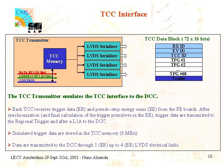
TCC Interface TCC Data Block ( 72 x 16 bits) TCC Transmitter LVDS Serializer TCC Memory DATA BUS (16 bits) ADDRESS BUS (18 bits) CONTROL LVDS Serializer BX ID EV ID TCC ID TPG #1 TPG #2 … TPG #68 Trailer The TCC Transmitter emulates the TCC interface to the DCC. Ø Each TCC receives trigger data (EB) and pseudo-strip energy sums (EE) from the FE boards. After synchronization (and final calculation of the trigger primitives in the EE), trigger data are transmitted to the Regional Trigger and after a L 1 A to the DCC. Ø Simulated trigger data are stored in the TCC memory (8 MBit). Ø Data are transmitted to the DCC through 1 (EB) up to 4 (EE) LVDS electrical links. LECC Amsterdam 29 Sept-3 Oct, 2003 - Nuno Almeida 10

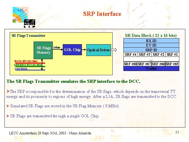
SRP Interface SR Data Block ( 21 x 16 bits) SR Flags Transmitter SR Flags Memory 16 bits GOL Chip Optical Driver DATA BUS (16 bits) ADDRESS BUS (18 bits) CONTROL BX ID EV ID SRP ID SRF #4 SRF #3 SRF #2 SRF #1 … SRF #68 SRF #67 SRF #66 SRF #65 Trailer The SR Flags Transmitter emulates the SRP interface to the DCC. ØThe SRP is responsible for the determination of the SR flags, which depends on the transversal TT energy and its proximity to regions of high energy. After a L 1 A, SR flags are transmitted to the DCC. Ø Simulated SR Flags are stored in the SR Flag Memory ( 8 MBit). Ø SR Flags are transmitted through a single GOL Chip. LECC Amsterdam 29 Sept-3 Oct, 2003 - Nuno Almeida 11

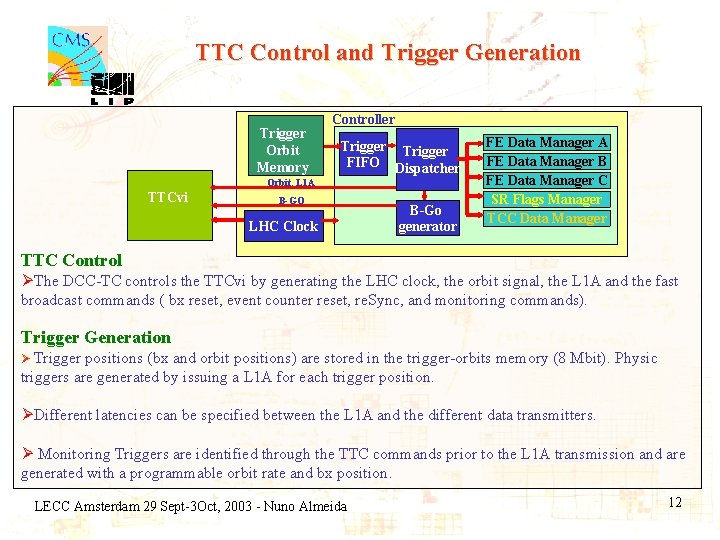
TTC Control and Trigger Generation Trigger Orbit Memory Controller Trigger FIFO Dispatcher Orbit, L 1 A TTCvi B-GO LHC Clock B-Go generator FE Data Manager A FE Data Manager B FE Data Manager C SR Flags Manager TCC Data Manager TTC Control ØThe DCC-TC controls the TTCvi by generating the LHC clock, the orbit signal, the L 1 A and the fast broadcast commands ( bx reset, event counter reset, re. Sync, and monitoring commands). Trigger Generation Ø Trigger positions (bx and orbit positions) are stored in the trigger-orbits memory (8 Mbit). Physic triggers are generated by issuing a L 1 A for each trigger position. ØDifferent latencies can be specified between the L 1 A and the different data transmitters. Ø Monitoring Triggers are identified through the TTC commands prior to the L 1 A transmission and are generated with a programmable orbit rate and bx position. LECC Amsterdam 29 Sept-3 Oct, 2003 - Nuno Almeida 12

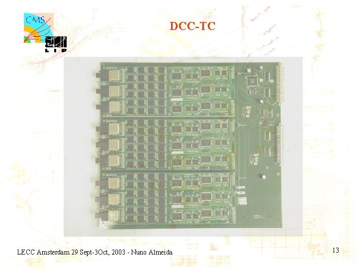
DCC-TC LECC Amsterdam 29 Sept-3 Oct, 2003 - Nuno Almeida 13

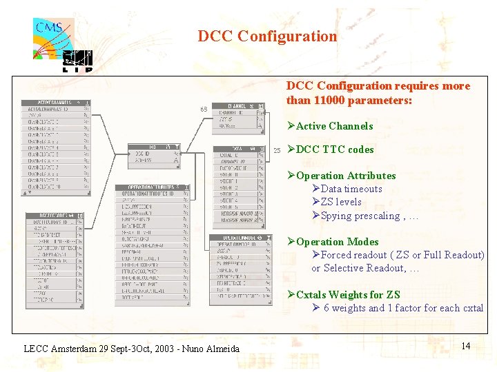
DCC Configuration requires more than 11000 parameters: ØActive Channels ØDCC TTC codes ØOperation Attributes ØData timeouts ØZS levels ØSpying prescaling , … ØOperation Modes ØForced readout ( ZS or Full Readout) or Selective Readout, … ØCxtals Weights for ZS Ø 6 weights and 1 factor for each cxtal LECC Amsterdam 29 Sept-3 Oct, 2003 - Nuno Almeida 14

Data Model and Raw Data Simulation ØSignal input: jets 50<pt<100 Ge. V at high luminosity (L~1034/cm 2/s ). ØFull ECAL detector simulation with ORCA. ØECAL raw data was simulated with an additional developed package and made persistent as ASCII files. Data Simulation Handling Ø Data files are parsed and software objects representing the DCC input data blocks instantiated. ØDifferent trigger conditions can be tested with the same data through a trigger generator. ØData are loaded in the DCC-TC memories and the expected DCC events are emultated based on the readout configuration of the DCC. LECC Amsterdam 29 Sept-3 Oct, 2003 - Nuno Almeida 15

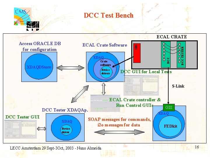
DCC Test Bench ECAL Crate Software DCC XDAQ Crate software XDAQDStore Device drivers DCC TESTER Access ORACLE DB for configuration SBS ECAL CRATE DCC GUI for Local Tests S-Link ECAL Crate controller & Run Control GUIs GIII DCC Tester XDAQAp. DCC Tester GUI XDAQ Device driver XDAQ SOAP messages for commands, i 2 o messages for data LECC Amsterdam 29 Sept-3 Oct, 2003 - Nuno Almeida FEDkit 16

Conclusions ØA prototype of the CMS ECAL Data Concentrator with full functionality was built and is under test. Ø A dedicated test system including a DCC Tester board emulating all DCC interfaces was developed. ØThe test system allows to validate the DCC hardware with simulated physics events at the highest L 1 trigger rate. LECC Amsterdam 29 Sept-3 Oct, 2003 - Nuno Almeida 17