DAS Data Acquisition Systems A DAS is required


- Slides: 28

DAS: Data Acquisition Systems • A DAS is required to allow an electronic system to get information on the external environment • The development of extremely miniaturized DASs capable of detecting a large number of different and inhomogeneous quantities is currently urged by emerging fields, such as robotics, security and health care. • This is giving a significant contribution to the request for analog and mixed signal integrated So. Cs • The design of a DAS involve architectures and specifications that recur in many other branches of analog and mixed signal microelectronic circuits. P. Bruschi – Microelectronic System Design 1

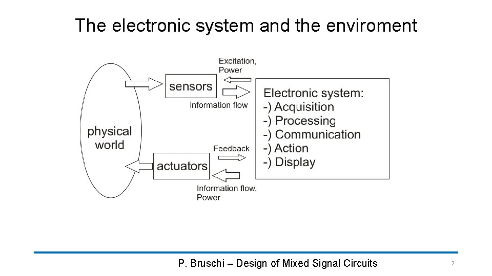
The electronic system and the enviroment P. Bruschi – Design of Mixed Signal Circuits 2

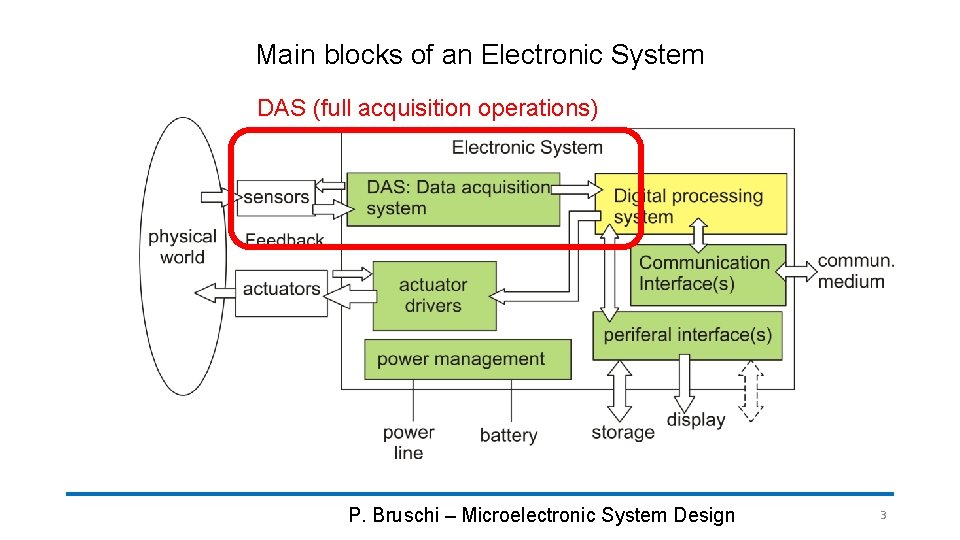
Main blocks of an Electronic System DAS (full acquisition operations) P. Bruschi – Microelectronic System Design 3

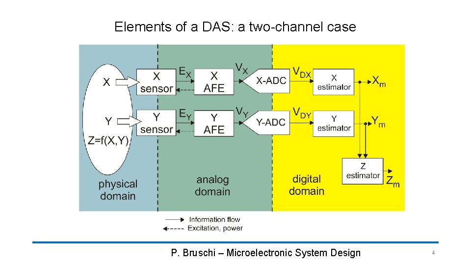
Elements of a DAS: a two-channel case P. Bruschi – Microelectronic System Design 4

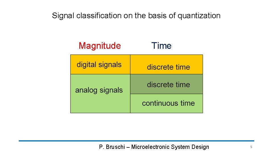
Signal classification on the basis of quantization Magnitude Time P. Bruschi – Microelectronic System Design 5

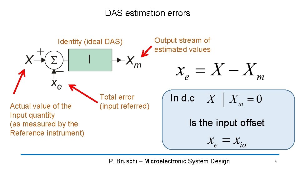
DAS estimation errors Identity (ideal DAS) Actual value of the Input quantity (as measured by the Reference instrument) Total error (input referred) Output stream of estimated values In d. c Is the input offset P. Bruschi – Microelectronic System Design 6

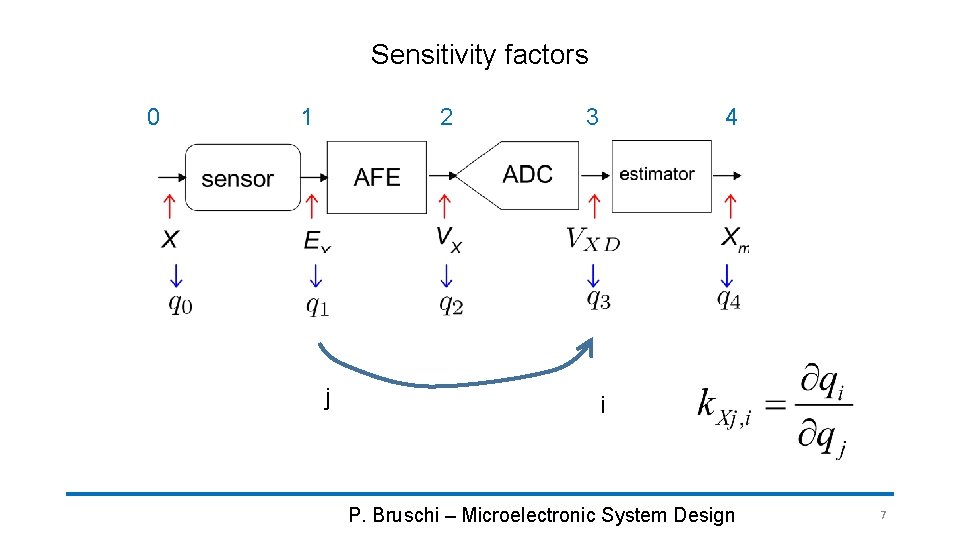
Sensitivity factors 0 1 2 j 3 4 i P. Bruschi – Microelectronic System Design 7

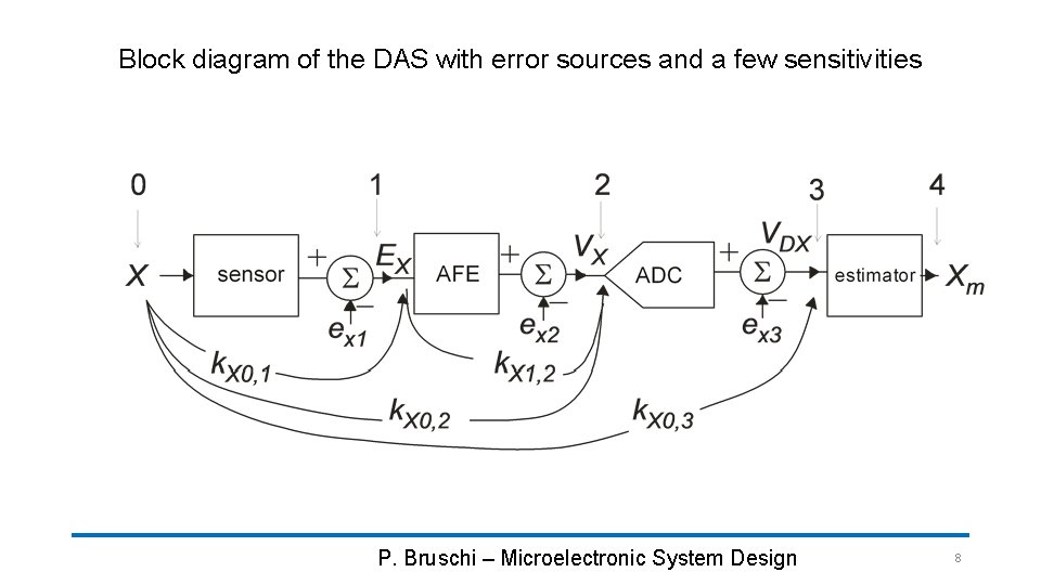
Block diagram of the DAS with error sources and a few sensitivities P. Bruschi – Microelectronic System Design 8

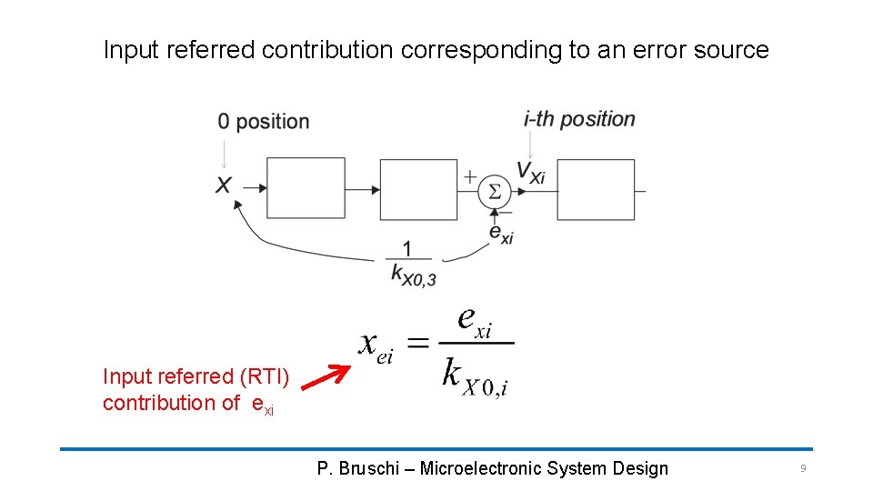
Input referred contribution corresponding to an error source Input referred (RTI) contribution of exi P. Bruschi – Microelectronic System Design 9

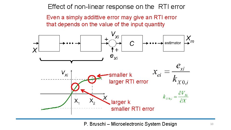
Effect of non-linear response on the RTI error Even a simply addittive error may give an RTI error that depends on the value of the input quantity smaller k larger RTI error larger k smaller RTI error P. Bruschi – Microelectronic System Design 10

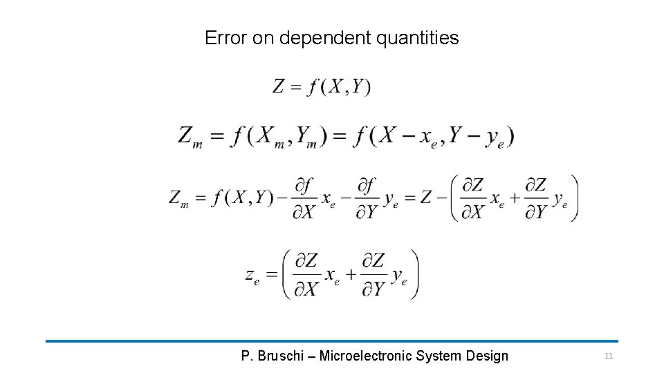
Error on dependent quantities P. Bruschi – Microelectronic System Design 11

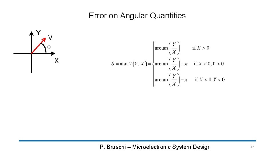
Error on Angular Quantities Y V q X P. Bruschi – Microelectronic System Design 12

Error on angular quantities P. Bruschi – Microelectronic System Design 13

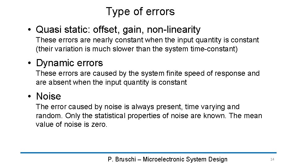
Type of errors • Quasi static: offset, gain, non-linearity These errors are nearly constant when the input quantity is constant (their variation is much slower than the system time-constant) • Dynamic errors These errors are caused by the system finite speed of response and are absent when the input quantity is constant • Noise The error caused by noise is always present, time varying and random. Only the statistical properties of noise are known. The mean value of noise is zero. P. Bruschi – Microelectronic System Design 14

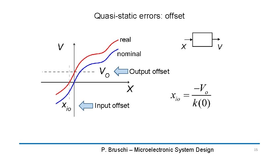
Quasi-static errors: offset Output offset Input offset P. Bruschi – Microelectronic System Design 15

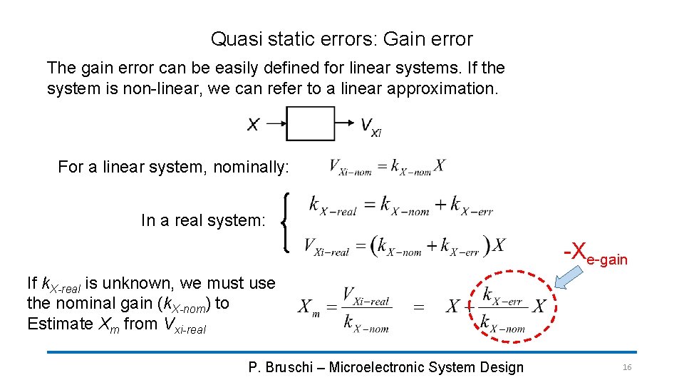
Quasi static errors: Gain error The gain error can be easily defined for linear systems. If the system is non-linear, we can refer to a linear approximation. For a linear system, nominally: In a real system: -Xe-gain If k. X-real is unknown, we must use the nominal gain (k. X-nom) to Estimate Xm from Vxi-real P. Bruschi – Microelectronic System Design 16

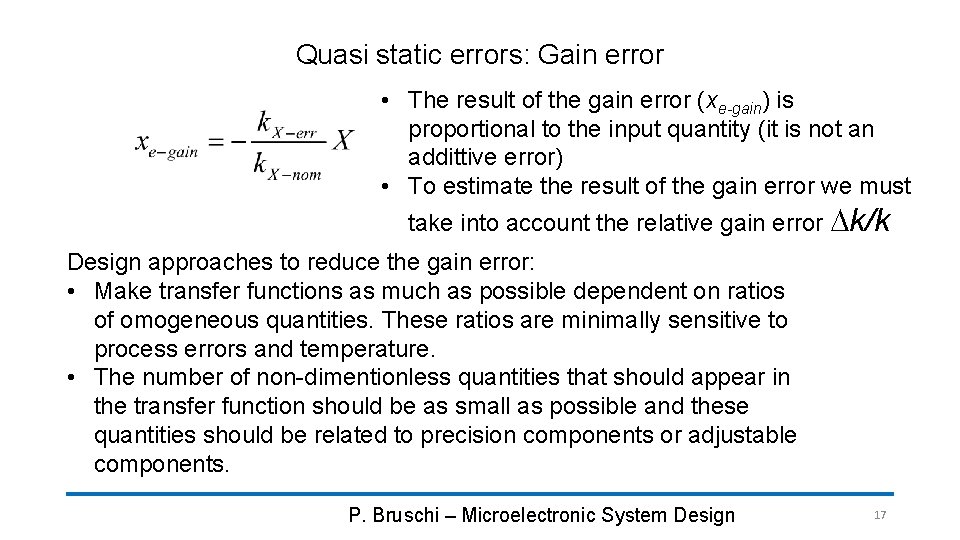
Quasi static errors: Gain error • The result of the gain error (xe-gain) is proportional to the input quantity (it is not an addittive error) • To estimate the result of the gain error we must take into account the relative gain error Dk/k Design approaches to reduce the gain error: • Make transfer functions as much as possible dependent on ratios of omogeneous quantities. These ratios are minimally sensitive to process errors and temperature. • The number of non-dimentionless quantities that should appear in the transfer function should be as small as possible and these quantities should be related to precision components or adjustable components. P. Bruschi – Microelectronic System Design 17

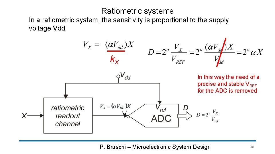
Ratiometric systems In a ratiometric system, the sensitivity is proportional to the supply voltage Vdd. k. X In this way the need of a precise and stable VREF for the ADC is removed VX P. Bruschi – Microelectronic System Design 18

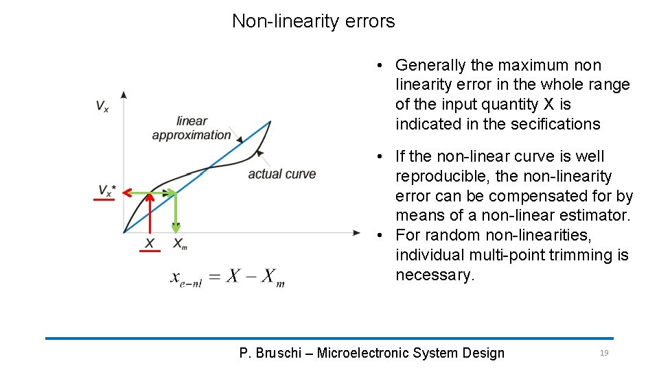
Non-linearity errors • Generally the maximum non linearity error in the whole range of the input quantity X is indicated in the secifications • If the non-linear curve is well reproducible, the non-linearity error can be compensated for by means of a non-linear estimator. • For random non-linearities, individual multi-point trimming is necessary. P. Bruschi – Microelectronic System Design 19

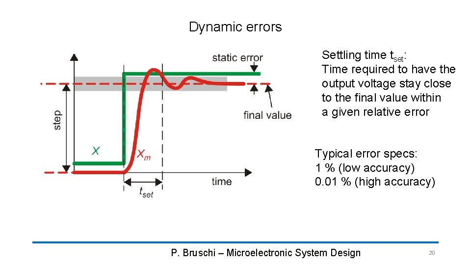
Dynamic errors Settling time tset: Time required to have the output voltage stay close to the final value within a given relative error Typical error specs: 1 % (low accuracy) 0. 01 % (high accuracy) P. Bruschi – Microelectronic System Design 20

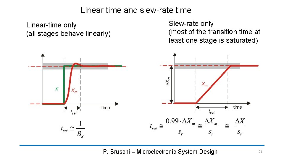
Linear time and slew-rate time Linear-time only (all stages behave linearly) Slew-rate only (most of the transition time at least one stage is saturated) P. Bruschi – Microelectronic System Design 21

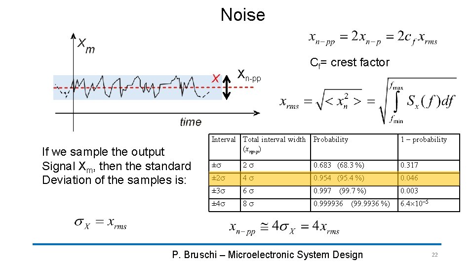
Noise Xn-pp If we sample the output Signal Xm, then the standard Deviation of the samples is: Cf= crest factor 1 - probability Interval Total interval width Probability (xnp-p) ±s 2 s 0. 683 (68. 3 %) 0. 317 ± 2 s 4 s 0. 954 (95. 4 %) 0. 046 ± 3 s 6 s 0. 997 0. 003 ± 4 s 8 s 0. 999936 (99. 7 %) (99. 9936 %) P. Bruschi – Microelectronic System Design 6. 4 10 -5 22

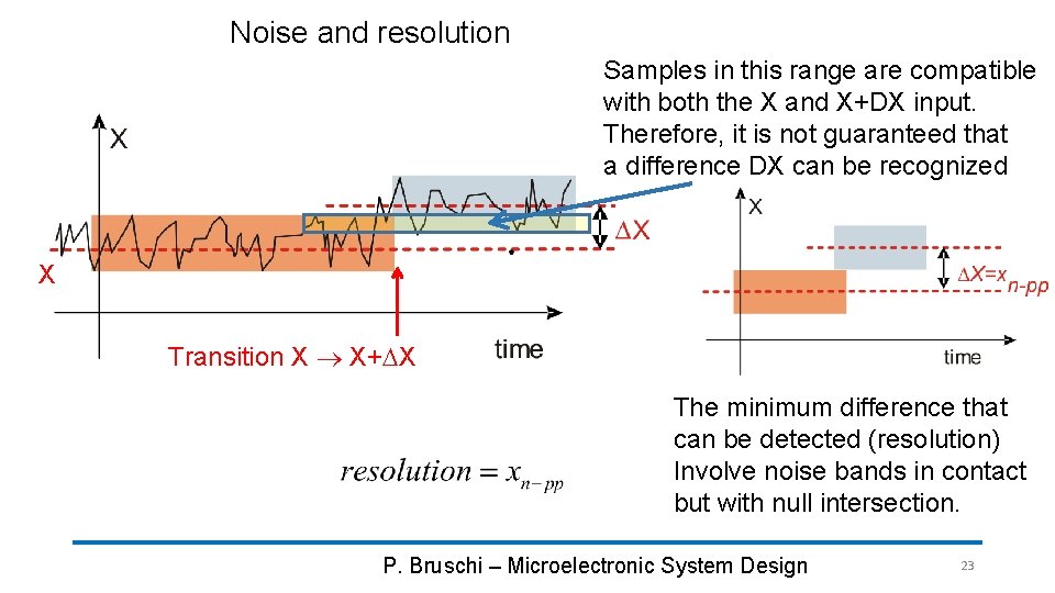
Noise and resolution Samples in this range are compatible with both the X and X+DX input. Therefore, it is not guaranteed that a difference DX can be recognized X Transition X X+DX The minimum difference that can be detected (resolution) Involve noise bands in contact but with null intersection. P. Bruschi – Microelectronic System Design 23

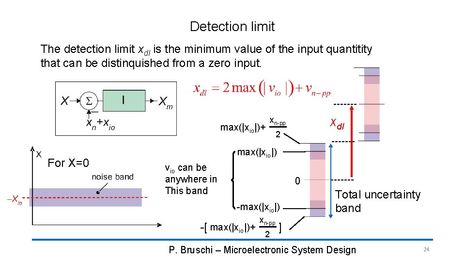
Detection limit The detection limit xdl is the minimum value of the input quantitity that can be distinquished from a zero input. max(|xio|)+ For X=0 xdl xn-pp 2 max(|xio|) vio can be anywhere in This band 0 -max(|xio|) -[ max(|xio|)+ xn-pp 2 Total uncertainty band ] P. Bruschi – Microelectronic System Design 24

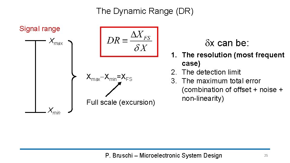
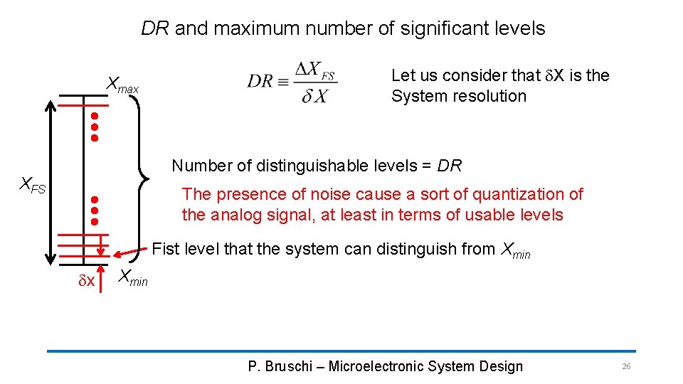
The Dynamic Range (DR) Signal range dx can be: Xmax-Xmin=XFS Xmin Full scale (excursion) 1. The resolution (most frequent case) 2. The detection limit 3. The maximum total error (combination of offset + noise + non-linearity) P. Bruschi – Microelectronic System Design 25

DR and maximum number of significant levels Xmax Let us consider that d. X is the System resolution Number of distinguishable levels = DR XFS The presence of noise cause a sort of quantization of the analog signal, at least in terms of usable levels Fist level that the system can distinguish from Xmin dx Xmin P. Bruschi – Microelectronic System Design 26

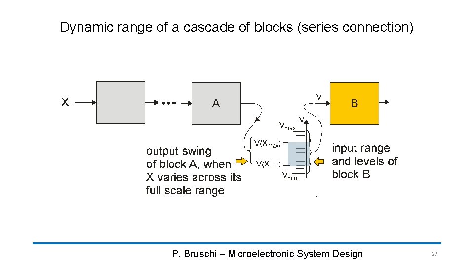
Dynamic range of a cascade of blocks (series connection) P. Bruschi – Microelectronic System Design 27

DR in series-connected blocks P. Bruschi – Microelectronic System Design 28