DAQ Update 1 DAQ Status DAQ was running
- Slides: 9

DAQ Update 1

DAQ Status • DAQ was running successfully and stably in ’ 07 beam time • Trigger bus scheme has proven to be very flexible – Added additional delayed trigger during beam time • Event rate of 6 Hz (m eg) + ~10 Hz calibration events can be handled easily – Max. DAQ rate now is 30 Hz, 50 Hz with firmware update – Dead time will be reduced by multi-event buffering through firmware update – DAQ rate will be even higher with DRS 4 (no calibration necessary) • DAQ rate was 0. 6 TB/day (7 MB/sec) – Reduction from 9 MB/event to <1 MB/event – Further reduction to ~50% by gzip compression – 100 TB disk available for 2008 2

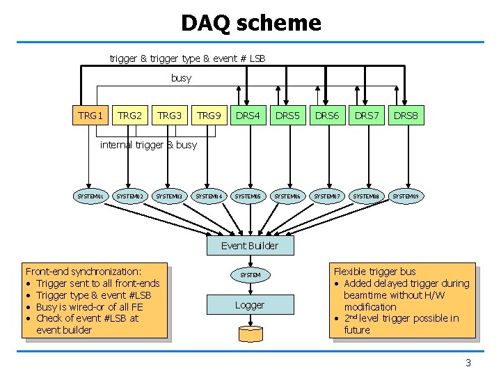
DAQ scheme trigger & trigger type & event # LSB busy TRG 1 TRG 2 TRG 3 TRG 9 DRS 4 DRS 5 DRS 6 DRS 7 DRS 8 SYSTEM 04 SYSTEM 05 SYSTEM 06 SYSTEM 07 SYSTEM 08 SYSTEM 09 internal trigger & busy SYSTEM 01 SYSTEM 02 SYSTEM 03 Event Builder Front-end synchronization: • Trigger sent to all front-ends • Trigger type & event #LSB • Busy is wired-or of all FE • Check of event #LSB at event builder SYSTEM Logger Flexible trigger bus • Added delayed trigger during beamtime without H/W modification • 2 nd level trigger possible in future 3

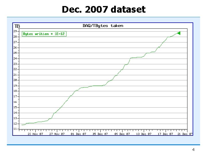
Dec. 2007 dataset TB 4

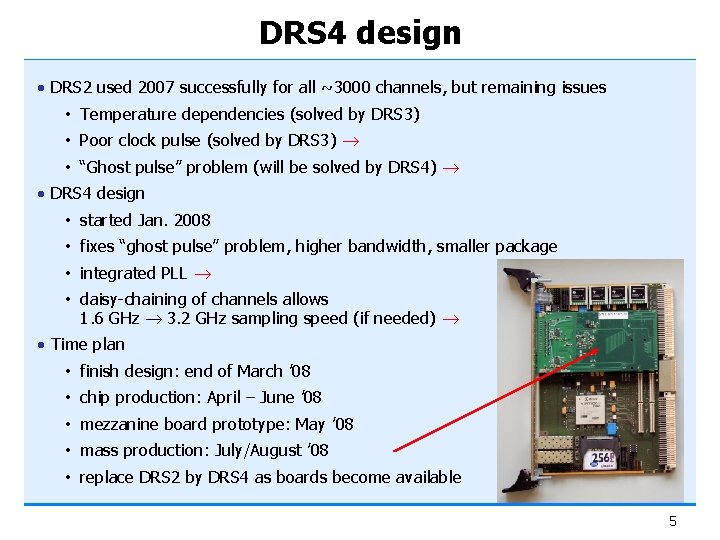
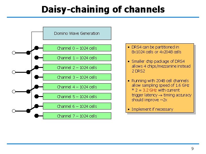
DRS 4 design • DRS 2 used 2007 successfully for all ~3000 channels, but remaining issues • Temperature dependencies (solved by DRS 3) • Poor clock pulse (solved by DRS 3) • “Ghost pulse” problem (will be solved by DRS 4) • DRS 4 design • started Jan. 2008 • fixes “ghost pulse” problem, higher bandwidth, smaller package • integrated PLL • daisy-chaining of channels allows 1. 6 GHz 3. 2 GHz sampling speed (if needed) • Time plan • finish design: end of March ’ 08 • chip production: April – June ’ 08 • mezzanine board prototype: May ’ 08 • mass production: July/August ’ 08 • replace DRS 2 by DRS 4 as boards become available 5

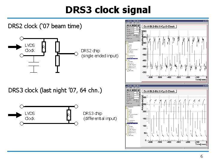
DRS 3 clock signal DRS 2 clock (‘ 07 beam time) LVDS Clock R DRS 2 chip (single ended input) DRS 3 clock (last night ’ 07, 64 chn. ) LVDS Clock R DRS 3 chip (differential input) 6

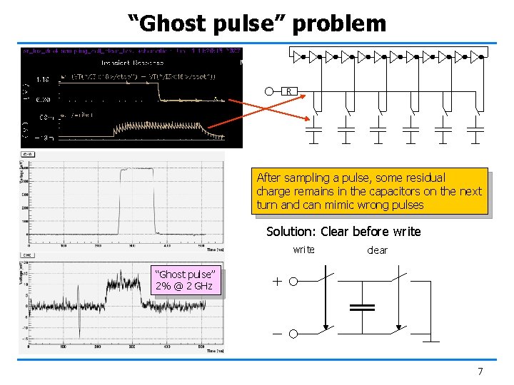
“Ghost pulse” problem R After sampling a pulse, some residual charge remains in the capacitors on the next turn and can mimic wrong pulses Solution: Clear before write clear “Ghost pulse” 2% @ 2 GHz 7

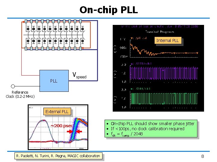
On-chip PLL Internal PLL Vspeed Reference Clock (0. 2 -2 MHz) External PLL ~200 psec R. Paoletti, N. Turini, R. Pegna, MAGIC collaboration • On-chip PLL should show smaller phase jitter • If <100 ps, no clock calibration required • fclk = fsamp / 2048 8

Daisy-chaining of channels Domino Wave Generation Channel 0 – 1024 cells Channel 1 – 1024 cells Channel 2 – 1024 cells Channel 3 – 1024 cells Channel 4 – 1024 cells Channel 5 – 1024 cells Channel 6 – 1024 cells • DRS 4 can be partitioned in 8 x 1024 cells or 4 x 2048 cells • Smaller chip package of DRS 4 allows 4 chips/mezzanine instead 2 DRS 2 • Running with 2048 cell channels allow sampling speed of 1. 6 GHz * 2 = 3. 2 GHz with current trigger latency timing accuracy should improve ~2 x • Implement if necessary Channel 7 – 1024 cells 9