
DAQ and Electronics presented by Gunther Haller Research
DAQ and Electronics presented by Gunther Haller Research Engineering Group Particle Physics and Astrophysics Division SLAC-Stanford University September 19, 2008 September 19, 08 Si. D Meeting Boulder 1 Gunther Haller haller@slac. stanford. edu
Overview Electronics Architecture Example front-end electronics options ECAL KPIX 7 Status GEM TKR Beam. Cal Muon (see Henry’s talk) DAQ LOI preparation September 19, 08 Si. D Meeting Boulder 2 Gunther Haller haller@slac. stanford. edu
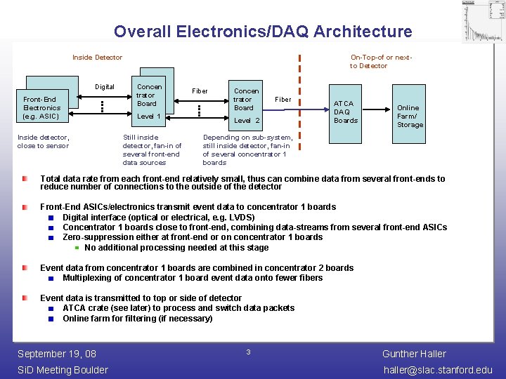
Overall Electronics/DAQ Architecture Inside Detector Digital Front-End Electronics (e. g. ASIC) Inside detector, close to sensor On-Top-of or nextto Detector Concen trator Board Level 1 Still inside detector, fan-in of several front-end data sources Fiber Concen trator Board Fiber Level 2 ATCA DAQ Boards Online Farm/ Storage Depending on sub-system, still inside detector, fan-in of several concentrator 1 boards Total data rate from each front-end relatively small, thus can combine data from several front-ends to reduce number of connections to the outside of the detector Front-End ASICs/electronics transmit event data to concentrator 1 boards Digital interface (optical or electrical, e. g. LVDS) Concentrator 1 boards close to front-end, combining data-streams from several front-end ASICs Zero-suppression either at front-end or on concentrator 1 boards No additional processing needed at this stage Event data from concentrator 1 boards are combined in concentrator 2 boards Multiplexing of concentrator 1 board event data onto fewer fibers Event data is transmitted to top or side of detector ATCA crate (see later) to process and switch data packets Online farm for filtering (if necessary) September 19, 08 Si. D Meeting Boulder 3 Gunther Haller haller@slac. stanford. edu
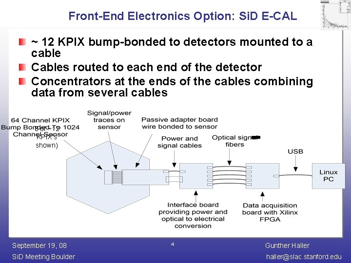
Front-End Electronics Option: Si. D E-CAL ~ 12 KPIX bump-bonded to detectors mounted to a cable Cables routed to each end of the detector Concentrators at the ends of the cables combining data from several cables 8 of ~12 KPIX’s shown) September 19, 08 Si. D Meeting Boulder 4 Gunther Haller haller@slac. stanford. edu
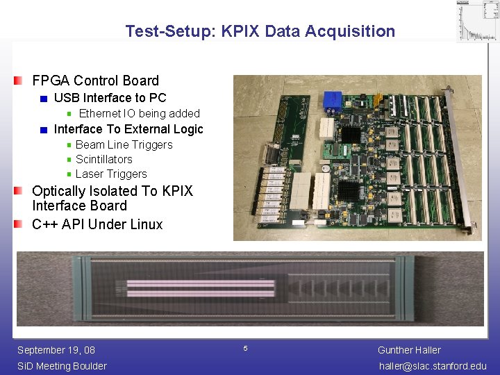
Test-Setup: KPIX Data Acquisition FPGA Control Board USB Interface to PC Ethernet IO being added Interface To External Logic Beam Line Triggers Scintillators Laser Triggers Optically Isolated To KPIX Interface Board C++ API Under Linux September 19, 08 Si. D Meeting Boulder 5 Gunther Haller haller@slac. stanford. edu
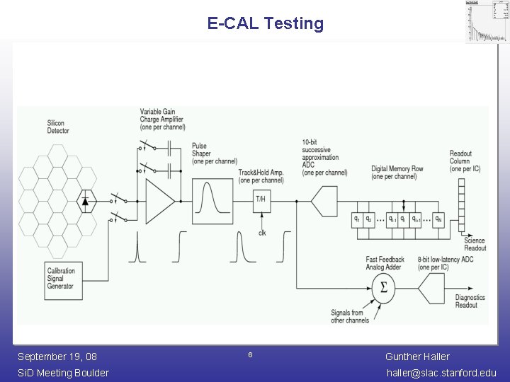
E-CAL Testing September 19, 08 Si. D Meeting Boulder 6 Gunther Haller haller@slac. stanford. edu
KPIX 7 Status Actively being used/tested GEM Chamber Tests @ UTA RPC Chamber Tests @ SLAC Planned E-Cal detector tests @ SLAC & Oregon Planned Tracker detector tests @ SLAC Improved routing of signal traces and power busses Digital crosstalk in readout traces eliminated Geographic influence on pixel performance eliminated Gained confidence for moving to larger number of pixels DC reset feature added Reduced ADC & Trigger noise by 50% Improved operation in asynchronous environments such as cosmic ray & source testing. September 19, 08 Si. D Meeting Boulder 7 Gunther Haller haller@slac. stanford. edu
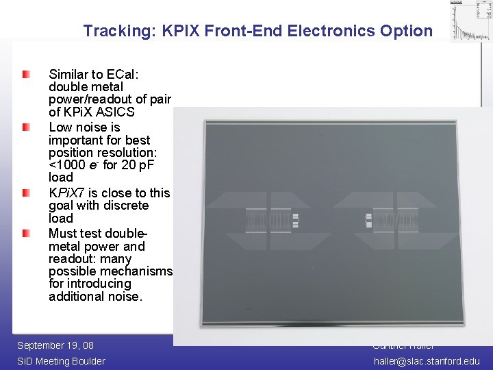
Tracking: KPIX Front-End Electronics Option Similar to ECal: double metal power/readout of pair of KPi. X ASICS Low noise is important for best position resolution: <1000 e- for 20 p. F load KPi. X 7 is close to this goal with discrete load Must test doublemetal power and readout: many possible mechanisms for introducing additional noise. September 19, 08 Si. D Meeting Boulder 8 Gunther Haller haller@slac. stanford. edu
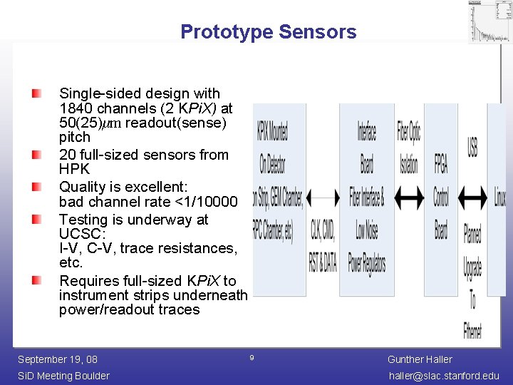
Prototype Sensors Single-sided design with 1840 channels (2 KPi. X) at 50(25)μm readout(sense) pitch 20 full-sized sensors from HPK Quality is excellent: bad channel rate <1/10000 Testing is underway at UCSC: I-V, C-V, trace resistances, etc. Requires full-sized KPi. X to instrument strips underneath power/readout traces September 19, 08 Si. D Meeting Boulder 9 Gunther Haller haller@slac. stanford. edu
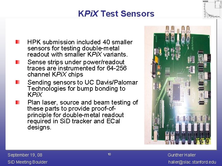
KPi. X Test Sensors HPK submission included 40 smaller sensors for testing double-metal readout with smaller KPi. X variants. Sense strips under power/readout traces are instrumented for 64 -256 channel KPi. X chips Sending sensors to UC Davis/Palomar Technologies for bump bonding to KPi. X Plan laser, source and beam testing of these parts to provide proof-ofprinciple for double-metal readout required in Si. D tracker and ECal designs. September 19, 08 Si. D Meeting Boulder 10 Gunther Haller haller@slac. stanford. edu
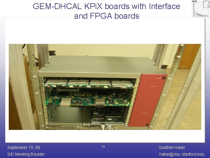
GEM-DHCAL KPi. X boards with Interface and FPGA boards September 19, 08 Si. D Meeting Boulder 11 Gunther Haller haller@slac. stanford. edu
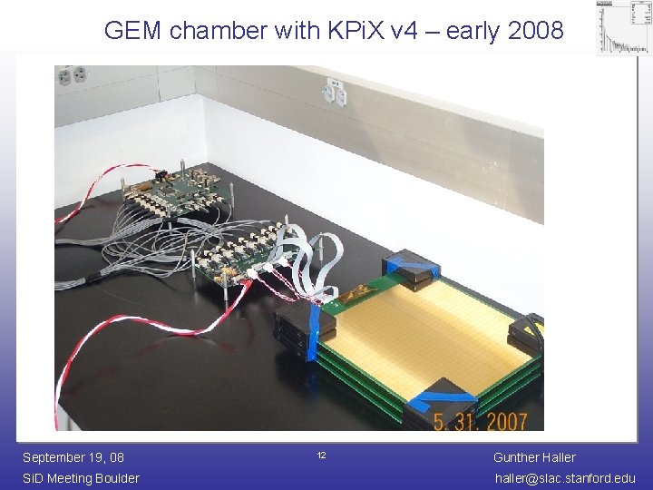
GEM chamber with KPi. X v 4 – early 2008 September 19, 08 Si. D Meeting Boulder 12 Gunther Haller haller@slac. stanford. edu
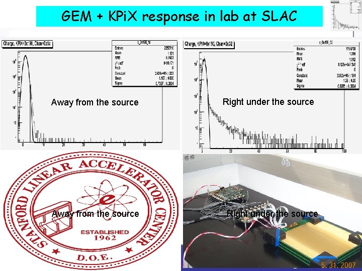
GEM + KPi. X response in lab at SLAC Right under the source Away from the source September 19, 08 Si. D Meeting Boulder Right under the source 13 Gunther Haller haller@slac. stanford. edu
FCAL: Beam. Cal Electronics Specs and Challenges High input rate (3. 25 MHz) High occupancy (100%) Large input signals (~40 p. C) Large input capacitance (~40 p. F detector + wires) High resolution (10 bits) Dual gain (50 x) for different modes of operation Low latency (~1 us) output for beam diagnostics High radiation (1 Mrad total dose) Integrated circuit in design at SLAC (Angel Abusleme) September 19, 08 Si. D Meeting Boulder 14 Gunther Haller haller@slac. stanford. edu
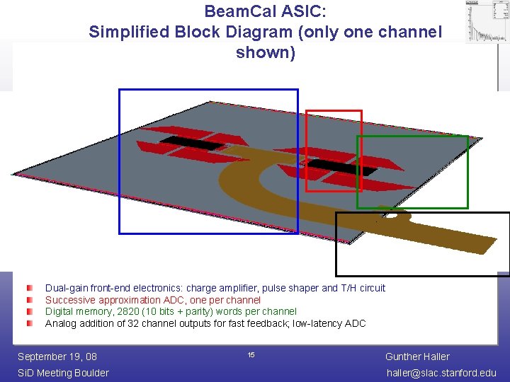
Beam. Cal ASIC: Simplified Block Diagram (only one channel shown) Dual-gain front-end electronics: charge amplifier, pulse shaper and T/H circuit Successive approximation ADC, one per channel Digital memory, 2820 (10 bits + parity) words per channel Analog addition of 32 channel outputs for fast feedback; low-latency ADC September 19, 08 Si. D Meeting Boulder 15 Gunther Haller haller@slac. stanford. edu
Beam. Cal Electronics: Techniques and Solutions gm/ID technique for precise analysis Time-variant filtering Differential circuitry Time budget (308 ns per event) sparingly used, quasitriangular weighting function: Switched capacitor filter for pulse shaper Slow reset Digital memory No leakage More choices against single-event effects High density in 0. 18 -um TSMC Front-end precharge to take advantage of output swing September 19, 08 Si. D Meeting Boulder 16 Gunther Haller haller@slac. stanford. edu
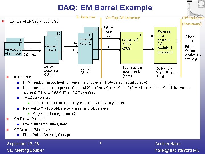
DAQ: EM Barrel Example In-Detector On-Top-Of-Detector E. g. Barrel EMCal, 54, 000 KPi. X 16 1 8 1 FE Module ~12 KPi. X’s 12 lines Concent rator 1 1 Concent 16 rator 2 In-Detector 36 1 1 Zero. Suppress & Sort (Stationary) 3 Gb/s Fiber 36 1 1 Crate of ATCA RCE’s Sub-System Event-Build (sort) Buffer /Sort Off-Detector Fraction of a crate: 1 IO module, 1 processor Fiber Filter, Online Analysis & Storage Detector. Wide Event. Build KPi. X Readout via two levels of concentrator boards (FPGA-based, reconfigurable) L 1 concentrator: zero-suppress. Sort total 20 hits/train/Kpix -> 20 hits * (2 words of 14 bits + 26 bit total system address) * 1 KHz * 96 KPIX; s = 12 Mbytes/sec To L 2 concentrator: Out of L 2 concentrator: 12 Mbytes/sec * 16 = 192 Mbytes/sec Readout to On-Top-Of-Detector crates via 3 Gbit/s fibers Only need 1 fiber, assume 2 On-Top-Of-Detector Event-Builder for sub-system Off-Detector (Stationary) Filter, Online-Analysis, Storage September 19, 08 Si. D Meeting Boulder 17 Gunther Haller haller@slac. stanford. edu
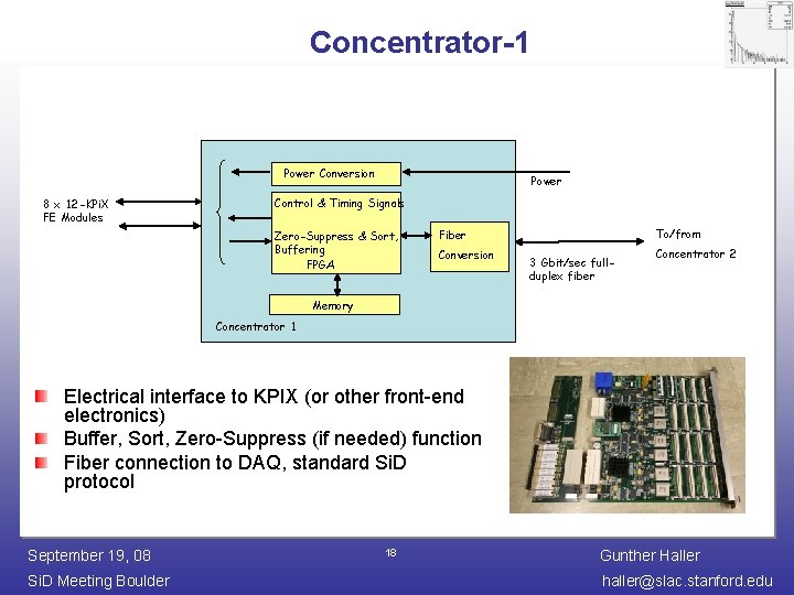
Concentrator-1 Power Conversion 8 x 12 -KPi. X FE Modules Power Control & Timing Signals Zero-Suppress & Sort, Buffering FPGA To/from Fiber Conversion 3 Gbit/sec fullduplex fiber Concentrator 2 Memory Concentrator 1 Electrical interface to KPIX (or other front-end electronics) Buffer, Sort, Zero-Suppress (if needed) function Fiber connection to DAQ, standard Si. D protocol September 19, 08 Si. D Meeting Boulder 18 Gunther Haller haller@slac. stanford. edu
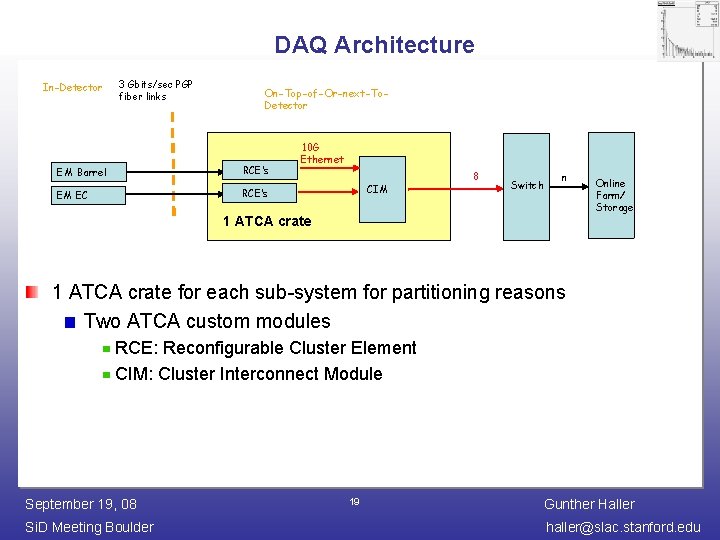
DAQ Architecture In-Detector 3 Gbits/sec PGP fiber links On-Top-of-Or-next-To. Detector RCE’s EM Barrel 10 G Ethernet CIM RCE’s EM EC 8 Switch n 1 ATCA crate Online Farm/ Storage 1 ATCA crate for each sub-system for partitioning reasons Two ATCA custom modules RCE: Reconfigurable Cluster Element CIM: Cluster Interconnect Module September 19, 08 Si. D Meeting Boulder 19 Gunther Haller haller@slac. stanford. edu
DAQ Sub-System Based on ATCA (Advanced Telecommunications Computing Architecture) Next generation of “carrier grade” communication equipment Driven by telecom industry Incorporates latest trends in high speed interconnect, next generation processors and improved Reliability, Availability, and Serviceability (RAS) Essentially instead of parallel bus backplanes, uses high-speed serial communication and advanced switch technology within and between modules, plus redundant power, etc September 19, 08 Si. D Meeting Boulder 20 Gunther Haller haller@slac. stanford. edu
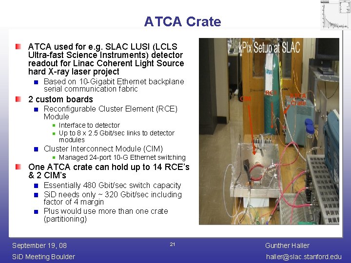
ATCA Crate ATCA used for e. g. SLAC LUSI (LCLS Ultra-fast Science Instruments) detector readout for Linac Coherent Light Source hard X-ray laser project Based on 10 -Gigabit Ethernet backplane serial communication fabric 2 custom boards CIM Reconfigurable Cluster Element (RCE) Module RCE ATCA Crate Interface to detector Up to 8 x 2. 5 Gbit/sec links to detector modules Cluster Interconnect Module (CIM) Managed 24 -port 10 -G Ethernet switching One ATCA crate can hold up to 14 RCE’s & 2 CIM’s Essentially 480 Gbit/sec switch capacity Si. D needs only ~ 320 Gbit/sec including factor of 4 margin Plus would use more than one crate (partitioning) September 19, 08 Si. D Meeting Boulder 21 Gunther Haller haller@slac. stanford. edu
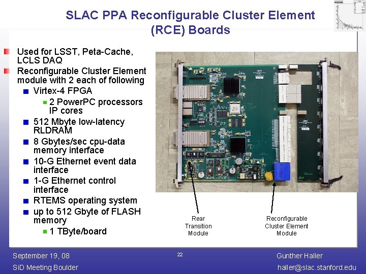
SLAC PPA Reconfigurable Cluster Element (RCE) Boards Used for LSST, Peta-Cache, LCLS DAQ Reconfigurable Cluster Element module with 2 each of following Virtex-4 FPGA 2 Power. PC processors IP cores 512 Mbyte low-latency RLDRAM 8 Gbytes/sec cpu-data memory interface 10 -G Ethernet event data interface 1 -G Ethernet control interface RTEMS operating system up to 512 Gbyte of FLASH memory 1 TByte/board September 19, 08 Si. D Meeting Boulder Rear Transition Module 22 Reconfigurable Cluster Element Module Gunther Haller haller@slac. stanford. edu
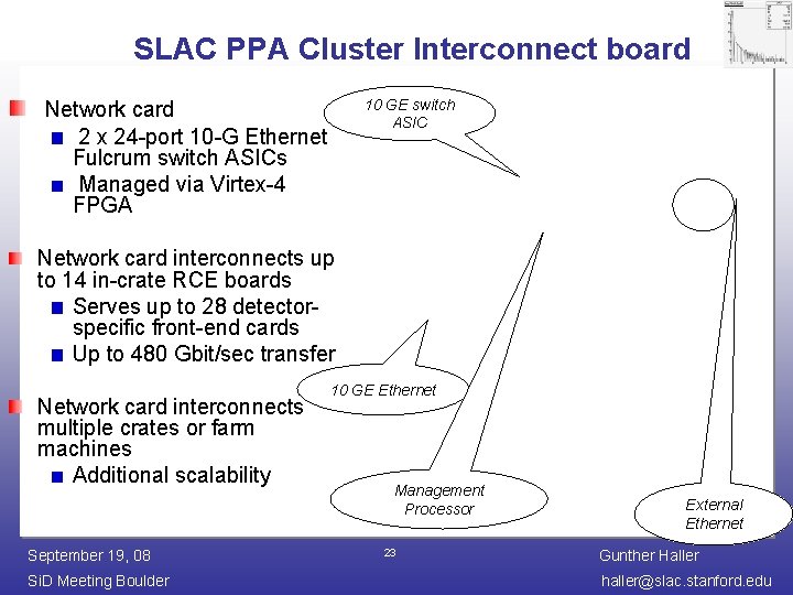
SLAC PPA Cluster Interconnect board 10 GE switch ASIC Network card 2 x 24 -port 10 -G Ethernet Fulcrum switch ASICs Managed via Virtex-4 FPGA Network card interconnects up to 14 in-crate RCE boards Serves up to 28 detectorspecific front-end cards Up to 480 Gbit/sec transfer Network card interconnects multiple crates or farm machines Additional scalability September 19, 08 Si. D Meeting Boulder 10 GE Ethernet Management Processor 23 External Ethernet Gunther Haller haller@slac. stanford. edu
LOI Preparation DAQ design being implemented for LCLS already higher performance than required for Si. D Good fit to Si. D, can write-up as is for LOI Areas to be addressed Data-management Filtering No filtering required in DAQ, large margin in throughput, scalable Could move event data to online farm/off-line for further filtering/analysis Still: investigate filtering in ATCA processors as well as in farm Offline data systems (processing/archiving) Needs volunteers September 19, 08 Si. D Meeting Boulder 24 Gunther Haller haller@slac. stanford. edu
Main Contributors (not complete) ECAL UC Oregon (David Strom, Ray Frey, Jim Brau, students) UC Davis (Mani Tripathi, Britt Holbrook, Richard Lander) SLAC (see below) Muon U. of Wisconsin (Henry Band) SLAC (see below) GEM University Of Texas @ Arlington (Andy White, Jae Yu, Jacob Smith) SLAC (see below) TKR SLAC ( Tim Nelson, Richard Partridge) SLAC (see below) Beam. Cal SLAC (Angel Abusleme) KPIX plus involved in above KPIX electronics systems SLAC (Ryan Herbst, Dieter Freytag, Marty Breidenbach, Gunther Haller, Angelo Dragone) UC Oregon (David Strom, Ray Frey) BNL (Velco Radeka) DAQ SLAC (Mike Huffer, Amedeo Perazzo, Matt Weaver, Chris O'Grady, Remi Machet, Ryan Herbst, Gunther Haller) September 19, 08 Si. D Meeting Boulder 25 Gunther Haller haller@slac. stanford. edu
- Slides: 25