CVD PCB first steps Overview Overhang Up to
CVD PCB, first steps
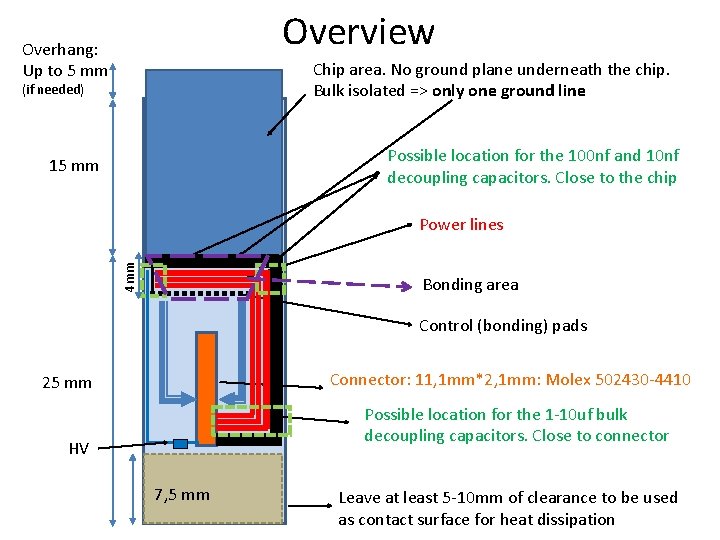
Overview Overhang: Up to 5 mm Chip area. No ground plane underneath the chip. Bulk isolated => only one ground line (if needed) Possible location for the 100 nf and 10 nf decoupling capacitors. Close to the chip 15 mm 4 mm Power lines Bonding area Control (bonding) pads Connector: 11, 1 mm*2, 1 mm: Molex 502430 -4410 25 mm Possible location for the 1 -10 uf bulk decoupling capacitors. Close to connector HV 7, 5 mm Leave at least 5 -10 mm of clearance to be used as contact surface for heat dissipation
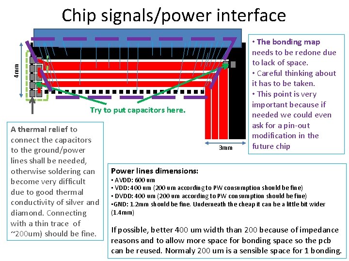
4 mm Chip signals/power interface Try to put capacitors here. A thermal relief to connect the capacitors to the ground/power lines shall be needed, otherwise soldering can become very difficult due to good thermal conductivity of silver and diamond. Connecting with a thin trace of ~200 um) should be fine. 3 mm • The bonding map needs to be redone due to lack of space. • Careful thinking about it has to be taken. • This point is very important because if needed we could even ask for a pin-out modification in the future chip Power lines dimensions: • AVDD: 600 um • VDD: 400 um (200 um according to PW consumption should be fine) • DVDD: 400 um (200 um according to PW consumption should be fine) • GND: 1. 2 mm should be fine. Underneath the cheap it can be a little bit wider (1. 4 mm) If possible, better 400 um width than 200 because of impedance reasons and to allow more space for bonding space so the pcb can be reused. Normaly 200 um is a sensible space for 1 bonding.
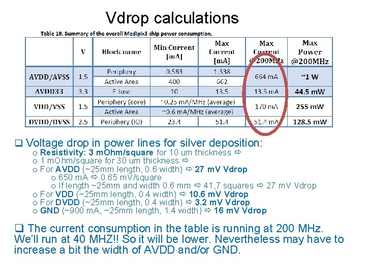
Vdrop calculations q Voltage drop in power lines for silver deposition: o Resistivity: 3 m. Ohm/square for 10 um thickness o 1 m. Ohm/square for 30 um thickness o For AVDD (~25 mm length, 0. 6 width) 27 m. V Vdrop o 650 m. A 0. 65 m. V/square o If length ~25 mm and width 0. 6 mm 41, 7 squares 27 m. V Vdrop o For VDD (~25 mm length, 0. 4 width) 10. 6 m. V Vdrop o For DVDD (~25 mm length, 0. 4 width) 3. 2 m. V Vdrop o GND (~900 m. A, ~25 mm length, 1. 4 width) 16 m. V Vdrop q The current consumption in the table is running at 200 MHz. We’ll run at 40 MHZ!! So it will be lower. Nevertheless may have to increase a bit the width of AVDD and/or GND.
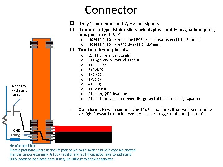
Connector q Only 1 connector for LV, HV and signals q Connector type: Molex slimstack, 44 pins, double row, 400 um pitch, max pin current 0. 3 A: o o 502430 -4410 => In diamond PCB end, it is narrower (11. 1 x 2. 1 mm) 502426 -4410 >> In FPC side (11. 9 x 2. 6 mm) o o o o o 21 (11 differential signals) 3 (single-ended control signals) 1 (3. 3 V line) 3 (AVDD) 1 (DVDD) 1 (VDD) 4 (GND) 1 (HV bias) 2 floating (HV clearance) 2 free. To be used to connect the ground of the decoupling capacitors q Total number of pins: 44 Needs to withstand 500 V o Open issue. How to connect the 10 u. F capacitors. It doesn’t seem to be straight forward to do it… We’ll have to struggle a bit, but just a bit. GND Floating HV bias and filter: Place a pad somewhere in the HV path so we could solder a wire in case we wanted bias the sensor externally. A 100 K resistor and a 22 nf càpacitor able to withstand 500 V needs to be placed here. It may be difficult to find de capacitor…
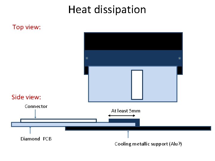
Heat dissipation Top view: Side view: Connector Diamond PCB At least 5 mm Cooling metallic support (Alu? )
Technical considerations • 200 um track and gap is the 'standard' that can easily be achieved. • 100 um gap/width is possible (so connecting to a 0. 3 mm pitch connector is feasible). Nevertheless, let’s try not to push to the limit. • No vias => one-side board without through-holes. • The chip might be powered only from one side. • The metal used is silver. It can get oxidized. Maybe we’ll have to think about a coating… • The square resistance is ~3 milli-ohm/square.
Ideas • No ground plane beneath the chip since the bulk of the device is isolated. Besides, silver can get very activated. • The 100 n. F and 10 n. F must be close to the chip, being the 10 n. F the closest. They have to be ceramic and the smallest possible (0402 should be fine). The bulk capacitors of 1 to 10 u. F must be close to the connector. If 10 u. F do not exist in 0402 size we could use lower capacitance values. They must also be ceramic.
Ideas • We can get rid of most of the DOUT differential pairs as we don’t read-out in parallel mode yet. According to the medipix manual only dataout[0] output is needed. This reduces the number of differential pairs to 11. • It would be nice to have a clearance area of 510 mm at least in one side of the diamond to use it as thermal conductive contact to a clamp. • We’ll have to check the performance of thermoplastic glue (or whatever is used) in diamond…
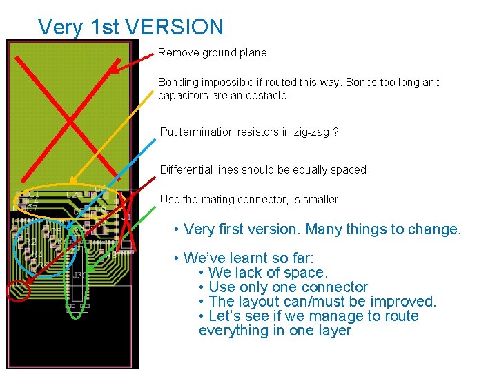
Very 1 st VERSION Remove ground plane. Bonding impossible if routed this way. Bonds too long and capacitors are an obstacle. Put termination resistors in zig-zag ? Differential lines should be equally spaced Use the mating connector, is smaller • Very first version. Many things to change. • We’ve learnt so far: • We lack of space. • Use only one connector • The layout can/must be improved. • Let’s see if we manage to route everything in one layer
- Slides: 10