Current MirrorsCurrent Amplifiers Specifications for current mirrors How


- Slides: 33
Current Mirrors/Current Amplifiers
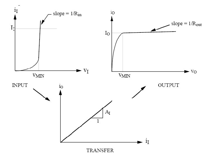
Specifications for current mirrors • How constant is io – Large ro • How large is vo range for which io is const – Small vmin • How accurate is mirror ratio – In the presence of process variations – Voltage supply variations – Environmental variations – Usage variations • Calculate, design strategy
Simple Current Mirrors Assuming square law model:
Simplest example
If m. Cox and VT matched: If v. DS matched: Current gain or mirror gain is controlled by geometric ratio, which can be made quite accurate
Use of transistor W to control current gains A better method, which I ask all you to follow, is to have the same W and L but use multipliers control the current. Also limit your mirror gain to be within one order of magnitude up or down.
Sources of Errors • Mismatches in W/L ratios – Use large W, L – Good layout • Mismatches in m. Cox – Large area, common centroid, higher order gradient cancellation • Mismatches in v. DS – Make v. DS the same • Mismatches in VT – Large area, cancel gradient, same W and L, same temperature, same V
l effect:
VT mismatch effect:
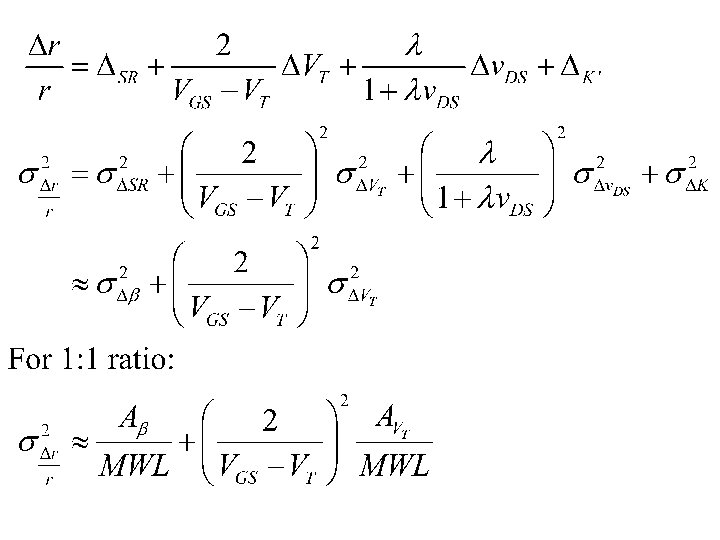
Sensitivity A systematic way of computing errors. r=
Note: common mode errors do not contribute to matching errors, only differential errors do Therefore, can take:
Strategies to reduce errors • Matching layout – PLI, common centroid, symmetry, gradient, … – Increased area • Matching operating conditions – VD, VS, VB, current densities, … use cascoding to fix VDS • Reduce the sensitivies – Use large VGS-VT – Make equivalent l small, make go small, use cascoding to reduce go
Straightforward layout to achieve mirror ratio of 4: Matching accuracy not good.
S G GS G GS Will have better matching But: only approximate common centroid no pli can be more compact HW: suggest a better layout for ratio of 4.
Cascoding M 1 and M 2 are the mirror pair that determines io. VDS 1 and VDS 2 matched go is small
Small signal model
Wilson Current Mirror go is small VDS 1 and VDS 2 not matched
Small signal circuit
Computation of rout
Improved Wilson Current Mirror
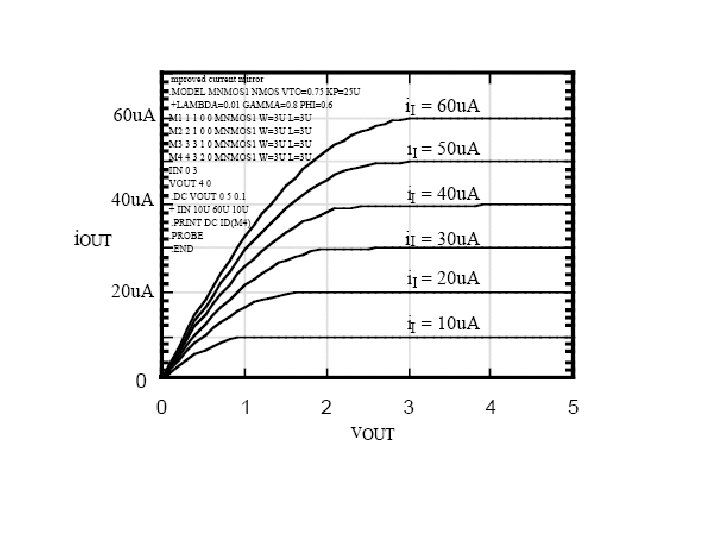
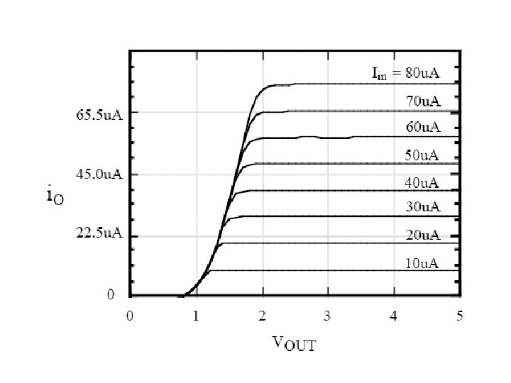
SPICE simulation
Regulated Cascode Current Mirror Same as the regulated cascoded curren sink VDS 2 is very stable with respect to vo, but not insensitive to Ireg change, not necessarily better matching
Implementation of IREG using a simple current mirror
Wide output voltage swings Ib Ib VT+2 Von 1/4 Von VT+Von Io >2 Von
Wide input and output voltage swings Ib Iin Von 1 1 + VT+Von – Ib VT+2 Von 1/4 VT+Von Io = Iin+Ib 1 >2 Von 1
Wide input and output voltage swings Iin Ib Ib + VT+2 Von Veb – VT-Veb +Von 1 Io = Iin 1/4 VT+Von Io >2 Von 1
A 1 -Volt, Two-Stage Op Amp Uses a bulk-driven differential input pair, wide swing current mirror load, and emitter follower level shifter
Bulk-driven current mirrors Increased vin range and vout range
Wide output voltage swings Ib Is Vin Vo. Q VT+Von Vo