Current Flow in Homogeneous Semiconductors Introduction Chapter 3


 are accelerated by")


 Where and is the conductivity due to electrons,")


 • Depend on whether you’re talking about majority carriers")


 • Particles")


 scattering • Vibrating atoms create acoustic waves in the crystal – Acoustic")


 scattering •")


")
")


 Chapter 3 Section 3. 5 Copyright © 2016 The")


 materials-")


 • There is no carrier concentration gradient, e. g.")


 and")


 and Fn(out) • Is made up by generation and recombination •")


 and there’s light")


 maxes out at some")


")


 at x=0 –")


- Slides: 187
Current Flow in Homogeneous Semiconductors: Introduction Chapter 3 Section 1 Copyright © 2016 The Mc. Graw-Hill Companies, Inc. Permission required for presentation or display
Introduction • In Chapter 2, learned how to find how many electrons and hole are available for conduction • This chapter: current flow • Two kinds of current in semiconductors – Drift: motion of charged particles in the presence of an electric field (same kind as in wires and resistors) – Diffusion: motion of particles due to concentration differences (an additional type of current in semiconductors) – Can have both at the same time
Drift Current Chapter 3 Section 2 Copyright © 2016 The Mc. Graw-Hill Companies, Inc. Permission required for presentation or display
Motion of the electron • Electrons and holes have thermal energy • Are moving, even at equilibrium • After collisions, new direction is random – No progress in any particular direction – Current is zero
When a field is applied • We know electrons (and holes) are accelerated by the field • They speed up until they collide – Then they lose energy and start accelerating again
Direction after collision is still random • But electron is accelerated in direction of the field • Over time makes progress in particular direction • It “drifts” to the right • This figure would represent a very high field Motion of electron under applied field
Drift under a normal field • Velocity induced by field is actually pretty small – For ≈10 V/cm, v≈107 cm/s (room temperature)
Definition of current • Amount of charge crossing a plane per unit time • Electron charge is negative – Electron in figure drifting to the right – Electron drift current In(drift) is going to the left
Hole drift • Hole is drifting to the left • Hole is positively charged • Hole drift current Ip(drift) is traveling to the left. • Both electron and hole drift current going to the left
End result
Current density • In semiconductors, useful to compare current density J rather than current I • Ohm’s Law: • Where ρ is resistivity (in ohm-cm), L is length and A is cross-sectional area
Let electric field be • I=JA and Therefore Or Where is the conductivity (in ohm-cm-1) Note we added subscript “drift” to J • Ohm’s Law in point form
Total current density (due to drift) Where and is the conductivity due to electrons, and is the conductivity due to holes.
No holes in a wire • Current in wire carried only by electrons • At left end, electron passes through the ohmic contact and jumps into a hole – Hole is annihilated – Opposing electron replaces hole that gets lost • At right end, electron jumps out of semiconductor into the wire
Find expressions for conductivity • Consider holes – We’ll use p for hole concentration – At equilibrium p=p 0 – Since current is flowing, it’s not equilibrium Apply a voltage to create a field in the –x direction
Force on the holes • Holes positively charged, they move to the left • Assume average drift velocity vdp • Total charge crossing area A in time dt is • Current is charge passing a plan per unit time so
Hole current density is • But we know and • So • And • Where μp is the “hole mobility” in cm 2/V-s
Mobility • Hole mobility: Electron mobility: • Conductivity due to holes • Conductivity due to electrons • Total drift current density • TOTAL CONDUCTIVITY
Key points • In the presence of an electric field, electrons and hole both drift, but in opposite directions • Since charges are opposite, both currents flow in the same direction • The conductivity due to each depends on – How many carriers there are (n or p) – How easily can the carriers move (mobility μn and μp • Conductivity of a semiconductor is
Carrier Mobility Chapter 3 Section 3 Copyright © 2016 The Mc. Graw-Hill Companies, Inc. Permission required for presentation or display
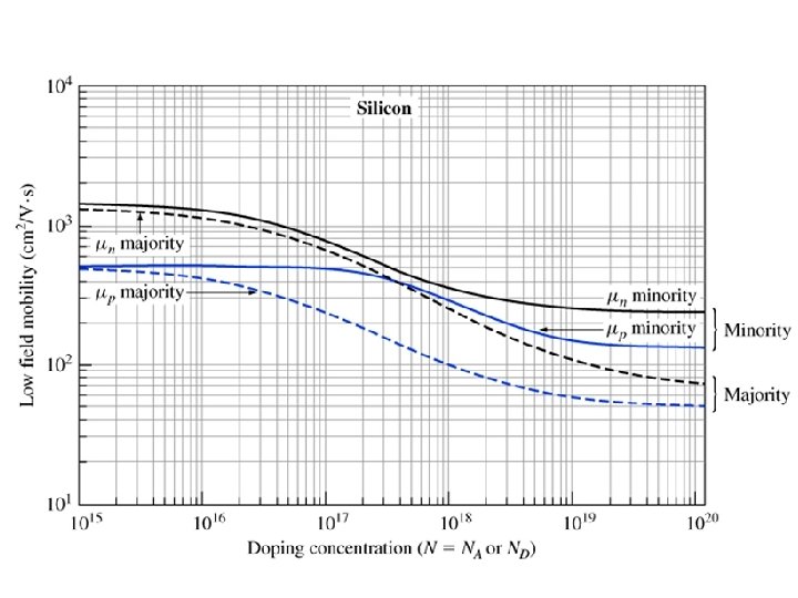
Conductivity depends on mobility • We saw in previous section that • Mobility depends on – Impurity (dopant) concentrations – Whether carrier is majority carrier or minority • Will give some results first – Discuss physics more in next sections
Mobility depends on doping • For non-compensated silicon, experimental results characterized by where N is the doping concentration (either ND or NA), and Nref and a are fitting parameters
Fitting parameters (silicon, low field) • Depend on whether you’re talking about majority carriers or minority carriers • Majority Carriers [1]: • Minority carriers [2]: [1] D. M. Caughey and R. Thomas “Carrier mobilities in silicon empirically related to doping and field”, Proc. IEEE 55, pp. 2192 -2193, (1967) [2] del Alamo, S. Swirhun and R. M. Swanson , “Measuring and modeling minority carrier transport in heavily doped silicon”, Solid State Electron, 28, pp. 47 -54 (1985).
• • At low doping, mobilities approach same values for majority, minority carries Mobilities decrease with increasing doping Electron mobilities higher than hole mobilities for a given doping Differences in majority, minority carriers increase with higher dopng
Example Compute the room temperature resistivity of intrinsic silicon, and compare that to uncompensated n- and p-type silicon doped with 1017 cm-3 donors (or acceptors). Assume n=n 0 and p=p 0. • Resistivity is given by and 1. Instrinsic silicon: n 0=p 0 = ni=1. 08 x 1010 cm-3. We find the mobilities from the chart : μ n=1330 cm 2/V·s and μp=495 cm 2/V·s.
Example, continued: n-type silicon • Since ND>>ni, and since all impurities are ionized and • Use chart to find mobilities
n-type example, continued • Note second term is negligible in this case • The doped silicon is considerably more conductive than the intrinsic case
Example, continued: p-type silicon • Since NA>>ni, and since all impurities are ionized and • Use chart to find mobilities
p-type example, continued • Note first term is negligible in this case • The p-type silicon is slightly less conductive than the n-type case with the same doping because current carried mostly by holes, which are less mobile
Key points so far • Conductivity depends on carrier mobilities • Mobility depends on doping • Mobility depends on whether you are talking about majority or minority carriers • Use fitted expressions to find the mobility, or use the chart – Make sure the chart and expressions are for the material you’re considering- the ones given here are for silicon • Next up: physics behind mobility differences
Carrier Scattering Chapter 3 Section 3. 1 Copyright © 2016 The Mc. Graw-Hill Companies, Inc. Permission required for presentation or display
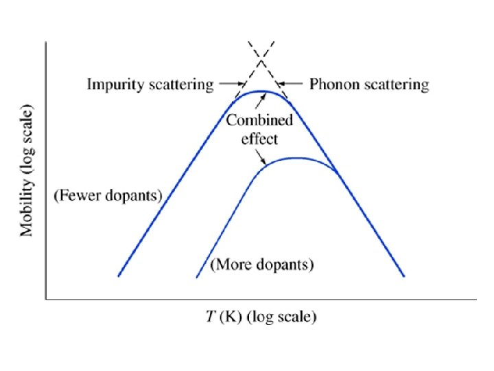
Recall mobility depends on drift velocity • Drift influenced by scattering (collisions) • Particles can collide with – Ionized impurities – Phonons • Drift velocity (and mobility) depends on mean free time between collisions
Ionized Impurity Scattering • Carriers are charged • Ionized impurities are charged • Carrier passing near an ionized impurity will get deflected • The higher the doping, the more often the scattering
Ionized Impurity Scattering, continued • Note that carriers are deflected by both positively and negatively ionized dopants • Mobility therefor depends on TOTAL doping ND+NA • Minority carrier minorities can be estimated from plot (even though plot is for uncompensated material) because usually ND>>NA or NA>>ND
Lattice (phonon) scattering • Vibrating atoms create acoustic waves in the crystal – Acoustic particles are called “phonons” 1 – They have energy – And wave vector – They can scatter carriers – Phonon energies small, usually less than 0. 1 e. V • Vibrations increase with temperature – Expect more phonons with increasing temperature – Expect more collisions – Expect mobility to go down as T goes up 1. See Supplement B to Part 1 for more details.
Key points • Carriers can be scattered by – Ionized impurities – Phonons (lattice vibrations) – Both • Higher doping reduces mobility • Higher temperature reduces mobility
Scattering Mobility Chapter 3 Section 3. 2 Copyright © 2016 The Mc. Graw-Hill Companies, Inc. Permission required for presentation or display
Scattering mobility • Recall force on particle due to electric field • Thus Talking about conduction, so use conductivity effective mass • Integrate both sides • Where t 0 is time of previous collision
Average over a large number of collisions • This is the drift velocity • Mean free time between collisions is • And • Recalling • And similarly , we get
We can see… • Mobility depends on conductivity effective mass • Depends also on scattering time • Scattering time depends on frequency of collisions with other particles (dopants, phonons) • These two mechanisms are independent and can be both going on at once
Example Find the mean free times between scattering, and , for intrinsic Si at room temperature. • Intrinsic means ND=NA=0 • Use • From chart (convert to mks units) • From table • And Similarly
Key points • Mobility depends on mean free time between collisions • More dopants means more collisions • Higher temperature means more phonon – Means more collisions • Have to account for both
Carrier Mobility Part A Chapter 3 Section 3. 3 Copyright © 2016 The Mc. Graw-Hill Companies, Inc. Permission required for presentation or display
We saw two scattering mechanisms – Ionized impurity scattering – Phonon (lattice) scattering • These both apply to majority and minority carriers • In addition, for carriers traveling in dopant impurity states, they get slowed down too – This applies only to majority carriers
Recall that under heavy doping • Impurities are close enough together to influence each other • Discrete state ED (or EA) spreads out into a mini-band • Electrons travelling in this band can be temporarily captured by dopant ions • Repeated catch-and-release slows carriers down • As doping increases, a greater fraction of majority carriers travels in this miniband
Important for majority carriers in uncompensated materials • In n-type material, the holes only travel in the valence band • If material is compensated, there can be another mini-band associated with the acceptor states – Hole mobility is affected by the acceptor doping only – Electron mobility affected by donor doping only – These two statements true only for impurity-band scattering • Still have regular ionized impurity scattering that affects both kinds of carriers – Plot we showed was for uncompensated material
Uncompensated Ga. As (minority carrier data not available)
Uncompensated Ge (minority carrier data not available)
Key points • For majority carriers, the mobility associated with impurity band scattering depends on the majority doping concentration only (e. g. μn depends on ND) – And minority mobility depends only on minority doping • Contrasts with ionized mobility scattering, where both majority and minority carriers are functions of ND+NA • Figures we showed are for uncompensated materials – In compensated materials, minority carriers will also be traveling in mini-band to some extent, so actual mobilities will be less than you’d get from the figure – Often ND>>NA or the reverse, in which case minority carrier band transport does not have a big effect
Key points, continued • When doping is not degenerate, majority and minority mobilities approach each other • As doping increases, majority carriers affected more, because of impurity-band transport, which affects only majority carriers
Temperature Dependence of Carrier Mobility Chapter 3 Section 3. 4 Copyright © 2016 The Mc. Graw-Hill Companies, Inc. Permission required for presentation or display
Mobility sensitive to temperature • We said earlier that phonon scattering increases with temperature – Increased T increases lattice vibrations – Causes more phonons – Lead to more lattice (phonon) scattering
Ionized impurity scattering • As temperature increases, average speed of carriers increases • Carrier moving fast, spend less time near impurity ions • Don’t scatter as much • Therefore ionized impurity scattering less important at high temperatures
Key points • At higher temperatures, phonon scattering dominates • At lower temperatures ionized impurity scattering dominates
High Field Effects (on mobility) Chapter 3 Section 3. 5 Copyright © 2016 The Mc. Graw-Hill Companies, Inc. Permission required for presentation or display
Mobility so far • We have been assuming that the velocity imparted by the electric field (drift velocity) was small compared to thermal speed (low field) • Drift velocity is then proportional to applied field
At high fields • Mean free time between collisions starts to saturate- colliding so often that increasing the field has less effect
Saturation velocity • As field increases, drift velocity vd increases sublinearly and appears to approach a limiting speed vsat • For both electrons and holes in Si, vsat≈107 cm/s • For Ge, vsat≈6 x 106 cm/s
Saturation due to optical phonon scattering • Recall phonons are lattice vibrations • Optical phonons 1 have higher energy than acoustic phonons (still are acoustic waves in both cases) • Possible under high fields for collisions to create optical phonons • Probability of this kind of collision high under large fields • Limits the velocity to – Ephonon≈0. 063 e. V for Si – Ephonon≈0. 034 e. V for Ga. As and Ge 1. For more details, see Supplement to Part 1 B
Example Estimate the value of the saturation velocity for electrons in Si. Make the following assumptions: 1) After each collision, an electron loses all of its kinetic energy 2) Electrons gain the kinetic energy Epho without intermediate collisions, i. e. the creation of optical phonons is the only scattering mechanism. 3) Between EK=0 and EK=m*v 2 MAX/2, the electrons are in the parabolic region of the E-K curve and so the concept of constant effective mass is valid. • Recall • From (1) and (2) Use conductivity effective mass since related to carrier motion (conduction)
Example, continued • For Si, Ephonon=0. 063 e. V and m*ce=0. 26 m 0 • Compare to measured value of 1 x 10⁷ – Discrepancy due to assumption (2): the electrons do make intermediate collisions
Comments on velocity saturation • Data in figure was for very pure (undoped) materials- with doping get more scattering and saturation velocity is reduced – Assumption (2) in example applies even less – Mean free time decreases because intermediate collisions become more important
What about Ga. As?
Explanation • Recall E-K diagram for Ga. As • At low field, carriers are mostly in lower minimum • At high fields, can be accelerated enough to scatter into the other minimum • Effective mass is higher there – Reduces drift velocity – Reduces saturation velocity
Key points • Under high electric fields – Carriers get so much kinetic energy they are colliding very often – Increase in drift not proportional to increase in electric field – Velocity saturates – For Ga. As, velocity decreases with increasing field after velocity peaks • due to scattering into a different E-K minimum that has different effective mass
Diffusion Current Chapter 3 Section 4 Copyright © 2016 The Mc. Graw-Hill Companies, Inc. Permission required for presentation or display
Two kinds of current • • We have discussed drift current Now we will look at diffusion current Diffusion current is not caused by a force Diffusion current arises when there is a gradient in the concentration of carriers
Consider a bar of semiconductor More electrons Fewer electrons • All electrons have some thermal energy • All electrons are moving • No field is applied • Electrons have no particular reason to move in any particular direction
• Half of these electrons are moving to the right • Half are moving to the left More electrons Fewer electrons Therefore, more electrons are moving from left to right across the plane x 0 than are crossing from right to left. Thus, a net current is flowing
Look at another way • Half of these electrons are moving to the right • Half are moving to the left Therefore, more electrons are moving from left to right across the plane x 0 than are crossing from right to left Thus, a net current is flowing
Let Fn be the net flux of electrons • Flux is net number of electrons crossing the plane • Let be the mean free path • Let be the mean free time between collisions
Flux is then • Factor of 2 comes from the fact that half of each population is going the other way • And n. L and n. R are the electron concentrations on the left and right hand sides of plane x 0
If the change in n is small in distance can be approximated as And Minus sign: says that electrons are flowing in direction of decreasing concentration Where D is the diffusion coefficient, defined as
Diffusion current density • Flux density Fn multiplied by the charge on the electron • For holes, we get Remember: F is not a force, it is a flux. There is no force at work here. Just thermal energy and variation in concentration.
Diffusion coefficient and mobility • Recall mobility μ described how easily a carrier moved through the lattice (from section on drift current) • Diffusion coefficient D describes how easily carriers diffuse These are known as the Einstein Relations
Diffusion coefficients for Si • Varies with doping
Compare D’s to μ’s D’s μ’s
You can apply a field, too • Possible to have a carrier concentration gradient and apply an electric field too • Total electron current is the sum of both: • Total hole current is
Use Einstein relation • To obtain • And similarly
Total current is the sum of the electron and hole currents • In p-type material – Electrons are minority carriers – Thus μn and Dn are the minority carrier mobilities and diffusion coefficients – And μp and Dp are the majority carrier mobilities and diffusion coefficients • Opposite for n-type material
In some devices (like resistors) • There is no carrier concentration gradient, e. g. • No diffusion current • Then it’s all drift, and Conductivity due to electrons Total conductivity Conductivity due to holes
Key points • Diffusion current arises from a gradient in the concentration of carriers – No force at work • Electrons and hole can both diffuse • Can have drift and diffusion current simultaneously
Carrier generation and recombination Chapter 3 Section 5 Copyright © 2016 The Mc. Graw-Hill Companies, Inc. Permission required for presentation or display
Electrons and holes • When temperature is not 0, there are electrons in the CB and holes in the VB • Have discussed creation of electrons and holes by doping with impurities • In this section we’ll discuss transitions between the bands
Generation • Generation: an electron acquires extra energy and is excited from the valence band to the conduction band – An electron “appears” in the conduction band – A hole “appears” in the valence band – The pair is called and electron-hole pair (EHP)
Recombination • Recombination: an electron in the conduction band loses energy and goes to the valence band to occupy a hole – The electron “disappears” from the conduction band – The hole “disappears” – The electron-hole pair is annihilated
Equilibrium vs. non-equilibrium • Generation and recombination occur at equal rates • Equilibrium concentrations n 0 and p 0 are constant • Under non-equilibrium conditions – Not necessarily true that n=n 0 or p=p 0 – The quantities n and p are the total electron and hole concentrations • There a number of generation and recombination processes- will discuss next
Band-to-band generation • This example involves absorption of a photon and a phonon
Band-to-band recombination • This example involves emission of multiple phonons
Two-step generation via acceptor 1. Electron absorbs phonon, goes to acceptor state 2. Electron absorbs photon, goes to conduction band 1
Two-step recombination via acceptor state 1. Electron temporarily trapped by acceptor state, emits photon 2. Electron returns to valence band, emitting phonon, and annihilating hole
Two-step generation via trap • Trap states are energy states deep in the forbidden band, usually result of crystal defects or unintentional impurities
Two-step recombination via trap
Key points • Generation and recombination processes are always going on all the time • At equilibrium, rate of generation equals rate of recombination and n=n 0 and p=p 0 • Phonons and photons are emitted or absorbed – Phonon have small energies – Photons have larger energies • Next: optical processes in semiconductors
Optical processes in semiconductors: absorption Chapter 3 Section 6. 1 Copyright © 2016 The Mc. Graw-Hill Companies, Inc. Permission required for presentation or display
At equilibrium • Electrons and holes constantly being generated and recombining • Generation rate equals recombination rate • Carrier concentrations are constant at n 0 and p 0
Non-equilibrium state • When light shines on a semiconductor, electron-hole pairs are generated – Creates “excess carriers” – above equilibrium, values
Compare to absorption by atom • In atom, energy states are discrete, only specific energies can be absorbed • In semiconductor, there is a range of energies that can be absorbed
Optical absorption • Photon energy E=hν • Conservation of energy: • In absorption, electron gets the energy from the photon – Photon is annihilated
Note • Final energy E 1>EC – Final state cannot be in forbidden band • Thus hν must be greater than Eg
Conservation of K • In addition to conservation of energy, there is another law that must be obeyed: wavevector K must be conserved. • Photons, however, have very small K – Thus after absorption event, electron’s K must be very close to initial K – Optical transitions must be vertical on E-K diagram
Conservation of K continued • This is a “direct gap” material
Indirect gap material • Transition from EV to EC requires change of energy and change of K • Energy comes from photon, but phonon is need to provide K • That requires a three-body collision- statistically unlikely
Direct vs indirect • Direct gap materials: good for optical devices. – Ga. As, In. P are examples • Indirect: poor for optical devices, inefficient emitters and absorbers – Si, Ge, Ga. P • Why is silicon widely used for solar cells? – Cheap.
Example • Verify that photons of interest have negligible wavevector compared to that of electrons at the edge of the Brillouin zone. Consider a red photon, with λ=620 nm (energy 2 e. V). Wavevector:
Electron at edge of Brillouin zone • Has wavevector of π/a (a is the lattice constant, say 0. 5 nm) • Ratio of K-vectors is
Shining light= non-equilibrium • An electron–hole pair is produced for every photon absorbed • Creates electrons and holes above the equilibrium concentrations – Excess carriers Δn and Δp
The excess carriers… • If the light is not uniform, but is brighter in some places than others, will create a gradient in carrier concentrations – Results in diffusion current • Even if the drift and diffusion currents are zero or even add to zero, as long as there are excess carriers, it’s not equilibrium • If you turn the light off, the excess carriers recombine with time and the sample returns to equilibrium
Key points • Must have conservation of E and of K • Photons have small K, meaning optical transitions must be vertical on E-K diagram • Direct-gap semiconductors good for optical devices – Indirect gap materials much less efficient • When light is shining on sample, it is not at equilibrium even if no voltage is applied
Optical processes in semiconductors: emission Chapter 3 Section 6. 2 Copyright © 2016 The Mc. Graw-Hill Companies, Inc. Permission required for presentation or display
Emission is inverse process to absorption • Electron initially in conduction band makes transition to lower energy – By conservation of energy, excess energy has to be given off • Could be photon • Could be phonon • Could be both – We’re talking about optical emission here But K must also be conserved! (Can’t see in this picture)
Conservation of K Direct gap Indirect gap
Key points • Emission requires electron at elevated state (e. g. conduction band) and an empty state at a lower energy (e. g. a hole in the valence band) for the electron to go to • Excess energy given off as photon (in optical transition) • Conservation of K still applies – Direct band gap materials good for LEDs and lasers – Indirect band gap materials poor emitters
Continuity Equations Chapter 3 Section 7 Copyright © 2016 The Mc. Graw-Hill Companies, Inc. Permission required for presentation or display
Continuity equations • Says particles are conserved • Tremendously useful for understanding electrical and electro-optical operation of devices • We’ll consider 1 -D case • In a wire, electrons flow in one end and out the other • In semiconductor, electrons and holes flow in and out – And they can be generated or they can recombine
Consider this 1 D semiconductor • Consider electrons here • Electron fluxes in and out: Fn(in) and Fn(out) – In general, these two not equal • Electrons generated in the region dx at rate Gn • Electrons disappear in region dx at rate Rn
Difference between Fn(in) and Fn(out) • Is made up by generation and recombination • Carriers may also pile up in the region or be depleted • In the differential length dx, rate of increase in n is
Multiple generation mechanisms • Carriers generated thermally or optically • Concentration could also be decreased by trapping of electrons in the volume (or increased by de-trapping) – Call these other mechanism “other”
Flux density is related to current density • Thus • Becomes Continuity equation for electrons and similarly Continuity equation for holes
Recall carrier concentrations • The total concentration is • And the equilibrium concentration n 0 is a constant, so And • And, let’s ignore the “other” generation processes and have
Now consider recombination • An electron at some elevated state has some average time associated with how long it takes (on average) to recombine – All things seek lower energies • Called the “carrier lifetime” – We’ll discuss in much more detail later • For a well-defined minority carrier lifetime τn, recombination rate is proportional to number of electrons available (in conduction band), so
Substituting into • Gives
Consider special case: equilibrium • No excess carriers, no current, and no optical generation • Then • Becomes
Combine results • To obtain • And similarly • Note that in general, Gopt, Δn and Δp are functions of position
Next, consider the current density • Consists of drift and diffusion • Continuity equations become
In three dimensions
Key points • Have to account for movement of electrons and holes as well as generation and recombination • Carriers can be generated or recombine thermally or optically, or by “other” mechanisms • Excess carrier concentration may vary with time and with position • We derived the continuity equations for electrons and holes • We’ll investigate this further in next section
Minority carrier lifetime Chapter 3 Section 8 Copyright © 2016 The Mc. Graw-Hill Companies, Inc. Permission required for presentation or display
Recall recombination • Electrons at elevated states tend to seek lower energies – They will recombine – Average time it take to recombine is called the minority carrier lifetime – Electrons in p-type material: τn – Holes in n-type material: τp • How to measure? Illuminate a sample, turn the light off, and measure rate of change of conductivity
Apparatus • Sample thin, absorption coefficient small – So carrier concentrations can be considered uniform throughout • Measure voltage (and thus current) through load RL
Experiment, continued • • Let resistance of sample be RS Let RL be small in comparison to RS Then measured current is ≈VA/RS Recalling RS=ρL/A and σ=1/ρ, • So i(t) is proportional to σ(t)
Recall the conductivity σ • Notice we put n and p instead of n 0 and po – There are n and p carriers to carry current • And we know • Thus
Continuing. . • We had • Which we can separate into an equilibrium (dark component) and a photoconductive component • Where the dark conductivity is • And the photoconductivity is
Consider a p-type direct-gap sample • There’s a field applied (VA) and there’s light
Note • Each generation event creates an electron-hole pair, and each recombination event gets rid of one (electrons or holes not created or destroyed by themselves) – Thus Δn=Δp • Generation rate does not necessarily equal recombination rate – Carriers may accumulate or deplete
In our example • We know Δn=Δp, so we just need to solve continuity equation for, say, Δn • Semiconductor is uniform and uniformly illuminated, and field is constant, so • And thus
We had the continuity equation • So result is • Solve it with initial conditions appropriate to the problem (we’ll do next episode)
And the photoconductivity is • But we know that Δn=Δp (carriers produces and annihilated in pairs), so
Key points so far • Excess carriers depend on generation and recombination, thermal and optical • When light is turned on, excess carriers are generated • When light is turned off, excess carriers decay due to recombination • We’re working toward minority carrier lifetime • Will do rise time and fall time separately- next
We were discussing this experiment • When light is turned on, excess carriers are generated, and the conductivity increases • When light is turned off, excess carriers decay through recombination and conductivity decreases
Rise time • We had derived • • For uniform illumination, thin sample Now apply initial conditions. Before t=0, sample is in the dark, and Δn=0 After t=0 solution is
After awhile • Carrier concentration saturates • We had • Let t go to infinity (or some long time)
Fall time • At some time t 0 turn off the light • Optical generation rate goes to 0 • Put Gopt=0 into • And solve to get
Comments • For n-type semiconductor with similar assumptions, get similar results but with τp and Δp • Recombination rate is (p-type) • Since usually n<<NA (p-type) • Where β is the probability that a given electron will recombine with a hole per unit time • Then • Or τn varies inversely with NA. The heavier the doping, the shorter the lifetime.
Photodetectors • Excess carrier concentration, and thus photoconductivity and photocurrent) maxes out at some value that depends on Gopt • Max current is proportional to the minority carrier lifetime. • As carrier lifetime increases, sensitivity of detector increase – But speed of response goes down (rise and fall times increase)
Example • Show that for a p-type semiconductor the average time an electron spends in the conduction band is equal to the time constant, τ n. Consider photoconductivity experiment, and at t=t 0=0 light is turned off. Then becomes
Average time spent in conduction band is • But • And we already solved for • So denominator is • And numerator is
Result
Experimental data for Si τp τn
Empirical expressions
Key points • Excess carrier concentration impacts photoconductivity • Maximum photocurrent proportional to minority carrier lifetime – Sensitivity depends on minority carrier lifetime – Also impacts rise and fall time (response speed) – These two have to be traded off in photodetector design • Minority carrier lifetime decreases with increasing doping concentration
Minority Carrier Diffusion Lengths Chapter 3 Section 9 Copyright © 2016 The Mc. Graw-Hill Companies, Inc. Permission required for presentation or display
Introduction • Recombination means carriers have a finite lifetime • They are, in general, moving during this time since they have some kinetic energy • This motion is diffusion- not caused by a field (they can drift too, but we’re talking about diffusion here) • How far can they go?
Consider a p-type sample • Illuminated from one side (light is on, steady state) • Light mostly absorbed near surface (we’ll assume here all absorption at surface) • Excess electrons and holes generated near the surface
Electrons will diffuse • Concentration of electrons much greater near surface than in bulk – Because it’s p-type, n 0 is small – Excess electron concentration Δn is noticeable compared to n 0 – Excess hole concentration Δp is negligible compared to p 0 – This is why we’re only interested in the minority carriers here
Electrons diffuse into the bulk • As they diffuse into the bulk, they recombine – There are lots of holes to recombine with, this is ptype • After light is turned on, Δn increases at surface • Steady state reached when excess electrons supplied by optical generation+ diffusion equals recombination rate
Use the continuity equation • For steady-state, • All electrons generated at surface, so Gop =0 for x >0 • Electron current given by • • No field applied, so and Jn(drift)=0
Continuity equation continued • We had • Or – No partial derivative anymore since no time variation anymore • Since • And n 0 is constant,
Solving • We had • Or • Boundary conditions: – Δn=Δn(0) at x=0 – Δn=0 at x=∞ • Solution to this second order differential equation
Define Diffusion Length • We had • Define • Then • Diffusion length is the average distance an electron diffuses before it recombines • For holes, is
Diffusion lengths Lp Ln
Key points • There is some distance, on the average, that a minority carrier will diffuse before recombining – Called the diffusion length • Depends on diffusion coefficient and lifetime – These both reduce with increased doping, so Ln and Lp do also • For silicon, diffusion lengths vary from around 1 mm for lightly doped to less than 1 μm for heavily doped materials • Diffusion lengths tend to be shorter in direct gap materials because the lifetimes are shorter
Quasi-Fermi Levels Chapter 3 Section 10 Copyright © 2016 The Mc. Graw-Hill Companies, Inc. Permission required for presentation or display
Introduction • At equilibrium, the Fermi level is constant – Can be used to determine equilibrium concentrations of electrons and holes – Fermi level is technically only defined at equilibrium • But, when excess carriers are present, we can create a “quasi-Fermi level” that reflects the non-equilibrium concentrations
Use analogous expression • For equilibrium, we had • So for non-equilibrium, let’s use These expressions only good for non-degenerate semiconductors
Rearranging • Let’s look at example of light illuminating one end of a p-type sample we examined earlier
The resulting quasi-Fermi level This end basically at equilibrium
Look at the current • For electrons • Using quasi-Fermi levels • Leads to
Continuing • We had • Now, the electric field is proportional to the gradient of the potential energy, which is EC, or • So from
Can express it differently • Previous result • Can be written as • Resembles Ohm’s law in point form! But been replaced with d(Efn/q)/dx • For holes has
These relations valid… • For any combination of drift and diffusion currents • When there is no diffusion current (dn/dx=dp/dx=0)
Key points • Fermi level only defined at equilibrium • Quasi-Fermi levels useful for non-equilibrium cases • They relate directly to carrier concentrations via normal formulas – As long as material is not degenerate • A gradient in Efn or Efp indicates there will be a net diffusion • Quasi-Fermi levels work for any combination of drift and diffusion
Homogeneous Semiconductors: Summary Chapter 3 Section 11 Copyright © 2016 The Mc. Graw-Hill Companies, Inc. Permission required for presentation or display
Two kinds of current in semiconductors • Drift: electrons and holes move under influence of an applied electric field • Diffusion: electrons and holes move to regions of lower concentration (no force at work)
Mobility μ • Mobility is a measure of how easily an electron or hole can move through the crystal • Directly relates to diffusion coefficient through Einstein relations • Mobility and diffusion coefficients decrease with increased doping • Use a chart to find values
Illumination creates electron-hole pairs • • • Must conserve both energy and wavevector Photons have plenty of energy but little K Phonons have plenty of K but little energy Optical transitions must be vertical on E-K diagrams Therefore direct-gap materials best for optical devices
Continuity equations • Have to account for carriers flowing in, flowing out, being created, and being destroyed • Hard to solve in closed form except for simple cases – We did some examples involving light shining on a sample
Minority carrier lifetimes • Lifetimes τn and τp are how long, on average, before a minority carrier recombines τp τn
Diffusion length • Diffusion lengths Ln and Lp are how far, on the average, does a minority carrier diffuse before recombining Lp Ln
Continuity equations again • When lifetime is well-defined, continuity equations become
Quasi-Fermi levels • Useful when sample not at equilibrium • They relate directly to total carrier concentrations • For non-degenerate semiconductors • And currents can be found from
Key points • We considered carrier motion and current in homogeneous semiconductors – Samples were assumed to have the same doping everywhere – Samples were assumed to be the same material everywhere • Next chapter: what happens when doping varies with position?