CSEE 217 GPU Architecture and Parallel Programming Lecture

![Two Access Patterns d_M d_N WIDTH Thread 1 Thread 2 WIDTH (a) d_M[Row*Width+k] (b) Two Access Patterns d_M d_N WIDTH Thread 1 Thread 2 WIDTH (a) d_M[Row*Width+k] (b)](https://slidetodoc.com/presentation_image_h/21af2d1245689ec56a5341467a8de506/image-18.jpg)

- Slides: 23

CS/EE 217 GPU Architecture and Parallel Programming Lecture 6: DRAM Bandwidth 1 ©Wen-mei W. Hwu and David Kirk/NVIDIA, University of Illinois, 2007 -2012

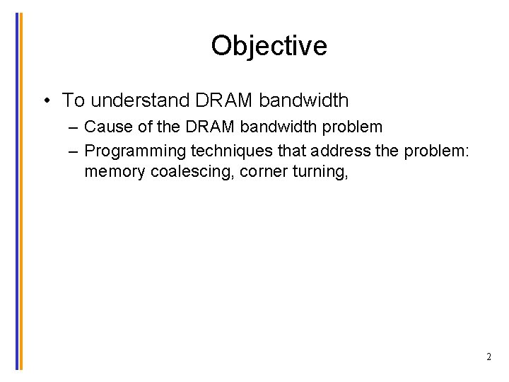
Objective • To understand DRAM bandwidth – Cause of the DRAM bandwidth problem – Programming techniques that address the problem: memory coalescing, corner turning, 2

Global Memory (DRAM) Bandwidth Ideal Reality 3

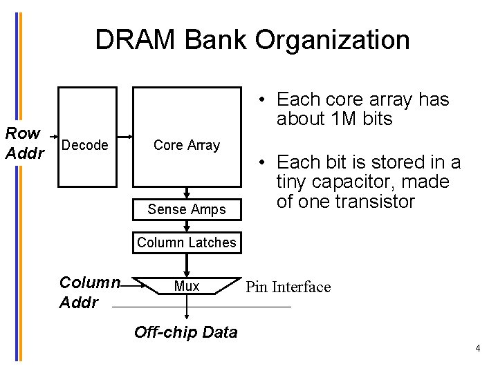
DRAM Bank Organization Row Addr Row Decoder • Each core array has about 1 M bits Memory Cell Core Array • Each bit is stored in a tiny capacitor, made of one transistor Sense Amps Column Latches Column Addr Wide Mux Pin Interface Narrow Off-chip Data 4

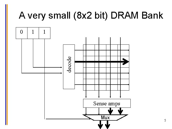
A very small (8 x 2 bit) DRAM Bank 1 1 decode 0 Sense amps Mux 5

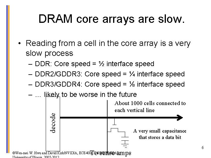
DRAM core arrays are slow. • Reading from a cell in the core array is a very slow process DDR: Core speed = ½ interface speed DDR 2/GDDR 3: Core speed = ¼ interface speed DDR 3/GDDR 4: Core speed = ⅛ interface speed … likely to be worse in the future decode – – About 1000 cells connected to each vertical line A very small capacitance that stores a data bit To sense amps ©Wen-mei W. Hwu and David Kirk/NVIDIA, ECE 408/CS 483/ECE 498 AL, 6

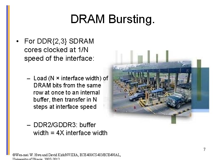
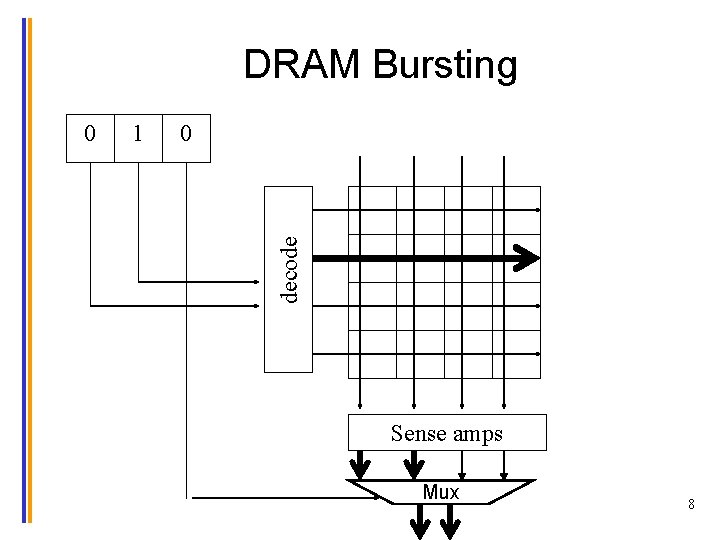
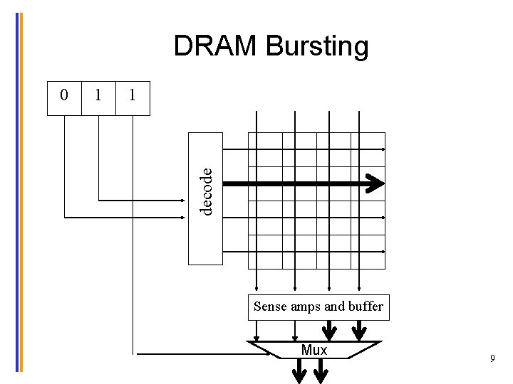
DRAM Bursting. • For DDR{2, 3} SDRAM cores clocked at 1/N speed of the interface: – Load (N × interface width) of DRAM bits from the same row at once to an internal buffer, then transfer in N steps at interface speed – DDR 2/GDDR 3: buffer width = 4 X interface width 7 ©Wen-mei W. Hwu and David Kirk/NVIDIA, ECE 408/CS 483/ECE 498 AL,

DRAM Bursting 1 0 decode 0 Sense amps Mux 8

DRAM Bursting 1 1 decode 0 Sense amps and buffer Mux 9

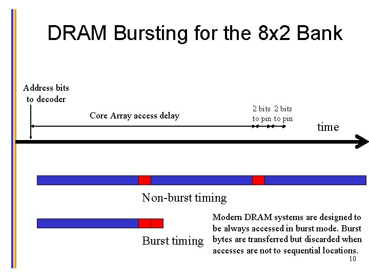
DRAM Bursting for the 8 x 2 Bank Address bits to decoder 2 bits to pin Core Array access delay time Non-burst timing Burst timing Modern DRAM systems are designed to be always accessed in burst mode. Burst bytes are transferred but discarded when accesses are not to sequential locations. 10

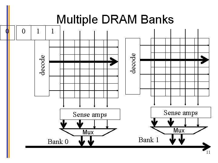
Multiple DRAM Banks 1 1 decode 0 Bank 0 Sense amps Mux Bank 1 11

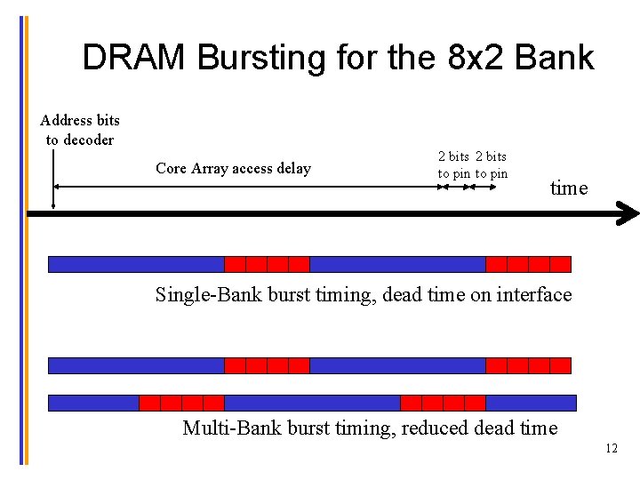
DRAM Bursting for the 8 x 2 Bank Address bits to decoder Core Array access delay 2 bits to pin time Single-Bank burst timing, dead time on interface Multi-Bank burst timing, reduced dead time 12

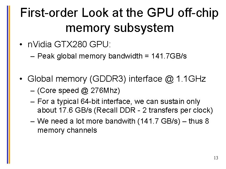
First-order Look at the GPU off-chip memory subsystem • n. Vidia GTX 280 GPU: – Peak global memory bandwidth = 141. 7 GB/s • Global memory (GDDR 3) interface @ 1. 1 GHz – (Core speed @ 276 Mhz) – For a typical 64 -bit interface, we can sustain only about 17. 6 GB/s (Recall DDR - 2 transfers per clock) – We need a lot more bandwith (141. 7 GB/s) – thus 8 memory channels 13

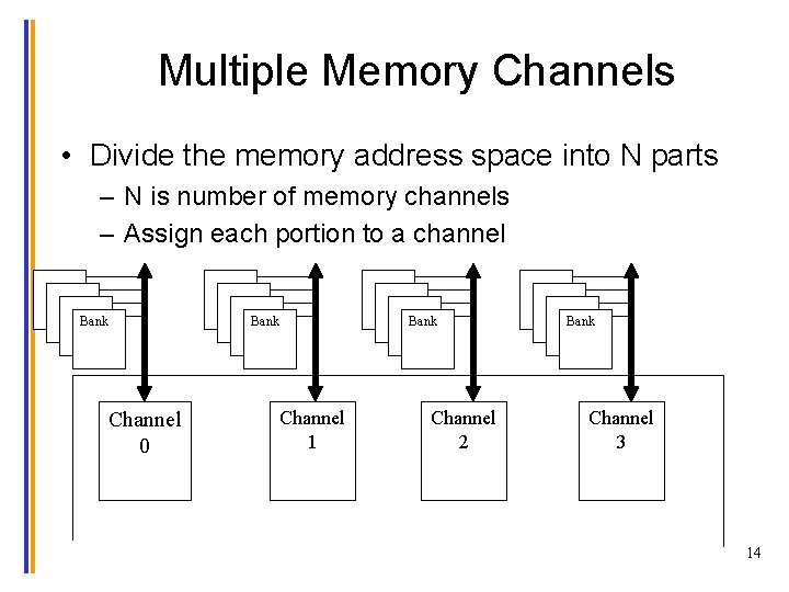
Multiple Memory Channels • Divide the memory address space into N parts – N is number of memory channels – Assign each portion to a channel Bank Channel 0 Bank Channel 1 Channel 2 Bank Channel 3 14

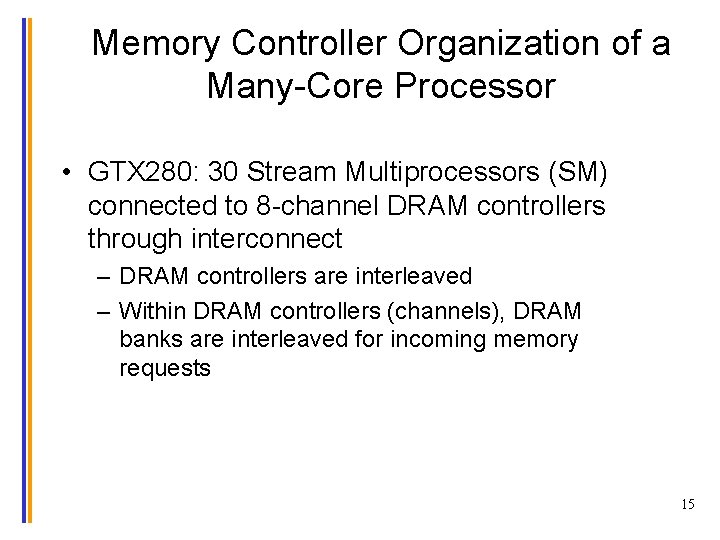
Memory Controller Organization of a Many-Core Processor • GTX 280: 30 Stream Multiprocessors (SM) connected to 8 -channel DRAM controllers through interconnect – DRAM controllers are interleaved – Within DRAM controllers (channels), DRAM banks are interleaved for incoming memory requests 15

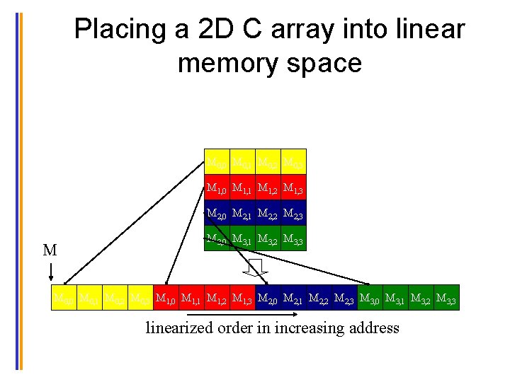
Placing a 2 D C array into linear memory space M 0, 0 M 0, 1 M 0, 2 M 0, 3 M 1, 0 M 1, 1 M 1, 2 M 1, 3 M 2, 0 M 2, 1 M 2, 2 M 2, 3 M M 3, 0 M 3, 1 M 3, 2 M 3, 3 M 0, 0 M 0, 1 M 0, 2 M 0, 3 M 1, 0 M 1, 1 M 1, 2 M 1, 3 M 2, 0 M 2, 1 M 2, 2 M 2, 3 M 3, 0 M 3, 1 M 3, 2 M 3, 3 linearized order in increasing address

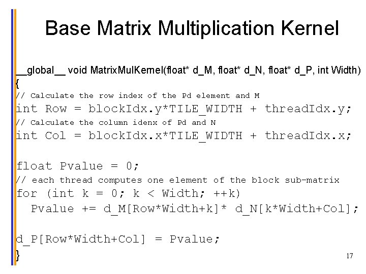
Base Matrix Multiplication Kernel __global__ void Matrix. Mul. Kernel(float* d_M, float* d_N, float* d_P, int Width) { // Calculate the row index of the Pd element and M int Row = block. Idx. y*TILE_WIDTH + thread. Idx. y; // Calculate the column idenx of Pd and N int Col = block. Idx. x*TILE_WIDTH + thread. Idx. x; float Pvalue = 0; // each thread computes one element of the block sub-matrix for (int k = 0; k < Width; ++k) Pvalue += d_M[Row*Width+k]* d_N[k*Width+Col]; d_P[Row*Width+Col] = Pvalue; } 17
![Two Access Patterns dM dN WIDTH Thread 1 Thread 2 WIDTH a dMRowWidthk b Two Access Patterns d_M d_N WIDTH Thread 1 Thread 2 WIDTH (a) d_M[Row*Width+k] (b)](https://slidetodoc.com/presentation_image_h/21af2d1245689ec56a5341467a8de506/image-18.jpg)
Two Access Patterns d_M d_N WIDTH Thread 1 Thread 2 WIDTH (a) d_M[Row*Width+k] (b) d_N[k*Width+Col] k is loop counter in the inner product loop of the kernel code 18

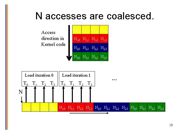
N accesses are coalesced. Access direction in Kernel code N 0, 0 N 0, 1 N 0, 2 N 0, 3 N 1, 0 N 1, 1 N 1, 2 N 1, 3 N 2, 0 N 2, 1 N 2, 2 N 2, 3 N 3, 0 N 3, 1 N 3, 2 N 3, 3 Load iteration 0 Load iteration 1 T 0 T 1 T 2 T 3 … N N 0, 0 N 0, 1 N 0, 2 N 0, 3 N 1, 0 N 1, 1 N 1, 2 N 1, 3 N 2, 0 N 2, 1 N 2, 2 N 2, 3 N 3, 0 N 3, 1 N 3, 2 N 3, 3 19

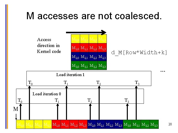
M accesses are not coalesced. M 0, 0 M 0, 1 M 0, 2 M 0, 3 Access direction in Kernel code M 1, 0 M 1, 1 M 1, 2 M 1, 3 M 2, 0 M 2, 1 M 2, 2 M 2, 3 d_M[Row*Width+k] M 3, 0 M 3, 1 M 3, 2 M 3, 3 … Load iteration 1 T 0 T 1 T 2 T 3 Load iteration 0 T 1 T 2 T 3 M M 0, 0 M 0, 1 M 0, 2 M 0, 3 M 1, 0 M 1, 1 M 1, 2 M 1, 3 M 2, 0 M 2, 1 M 2, 2 M 2, 3 M 3, 0 M 3, 1 M 3, 2 M 3, 3 20

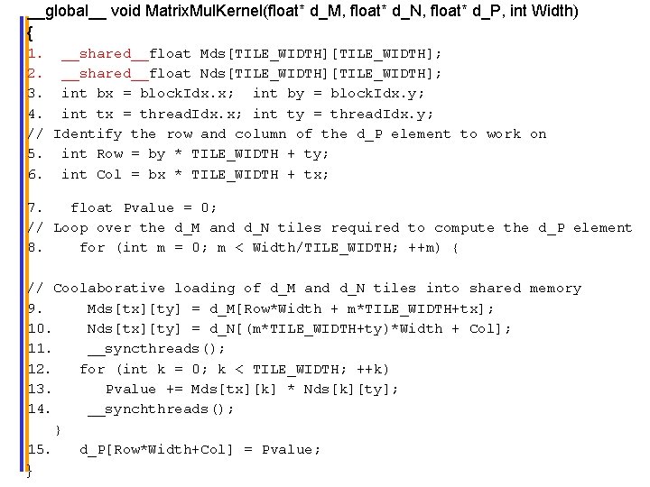
__global__ void Matrix. Mul. Kernel(float* d_M, float* d_N, float* d_P, int Width) { 1. __shared__float Mds[TILE_WIDTH]; 2. __shared__float Nds[TILE_WIDTH]; 3. int bx = block. Idx. x; int by = block. Idx. y; 4. int tx = thread. Idx. x; int ty = thread. Idx. y; // Identify the row and column of the d_P element to work on 5. int Row = by * TILE_WIDTH + ty; 6. int Col = bx * TILE_WIDTH + tx; 7. float Pvalue = 0; // Loop over the d_M and d_N tiles required to compute the d_P element 8. for (int m = 0; m < Width/TILE_WIDTH; ++m) { // Coolaborative loading of d_M and d_N tiles into shared memory 9. Mds[tx][ty] = d_M[Row*Width + m*TILE_WIDTH+tx]; 10. Nds[tx][ty] = d_N[(m*TILE_WIDTH+ty)*Width + Col]; 11. __syncthreads(); 12. for (int k = 0; k < TILE_WIDTH; ++k) 13. Pvalue += Mds[tx][k] * Nds[k][ty]; 14. __synchthreads(); } 15. d_P[Row*Width+Col] = Pvalue; }

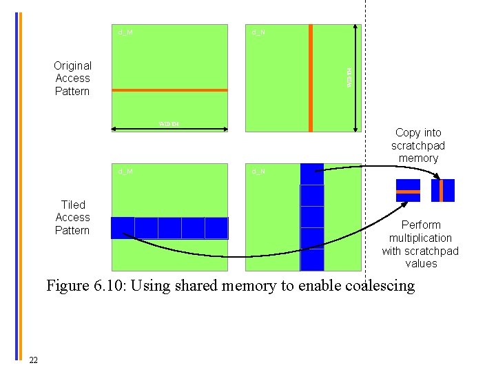
d_M d_N WIDTH Original Access Pattern WIDTH d_M Tiled Access Pattern Copy into scratchpad memory d_N Perform multiplication with scratchpad values Figure 6. 10: Using shared memory to enable coalescing 22

ANY MORE QUESTIONS? READ CHAPTER 6 23