CSE 675 02 Introduction to Computer Architecture Cache

- Slides: 25

CSE 675. 02: Introduction to Computer Architecture Cache Memory Presentation I Gojko Babić 08/12/2005

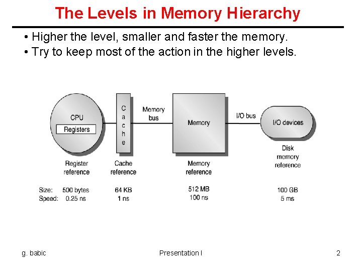
The Levels in Memory Hierarchy • Higher the level, smaller and faster the memory. • Try to keep most of the action in the higher levels. g. babic Presentation I 2

Principle of Locality The principle of locality is the most important program property that is exploited in many parts of memory hierarchy. The principle of locality states that programs tend to reuse instructions and data they have used recently. There are two different types of locality: – temporal locality – recently accessed locations in the main memory are likely to be accessed in the near future, – spatial locality – locations in the main memory near one another tend to be referenced close together in time. Principle of locality applies more strongly to code accesses than data accesses. An implication of principle of locality is that we can predict with reasonable accuracy what instructions and data a program will use in near future based on its accesses in the recent past. g. babic Presentation I 3

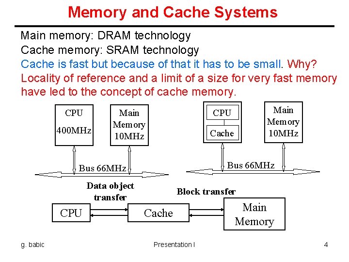
Memory and Cache Systems Main memory: DRAM technology Cache memory: SRAM technology Cache is fast but because of that it has to be small. Why? Locality of reference and a limit of a size for very fast memory have led to the concept of cache memory. CPU 400 MHz Main Memory 10 MHz Cache Bus 66 MHz Data object transfer CPU g. babic Main Memory 10 MHz CPU Block transfer Cache Presentation I Main Memory 4

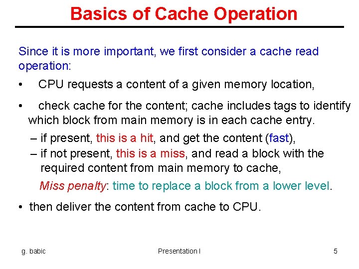
Basics of Cache Operation Since it is more important, we first consider a cache read operation: • • CPU requests a content of a given memory location, check cache for the content; cache includes tags to identify which block from main memory is in each cache entry. – if present, this is a hit, and get the content (fast), – if not present, this is a miss, and read a block with the required content from main memory to cache, Miss penalty: time to replace a block from a lower level. • then deliver the content from cache to CPU. g. babic Presentation I 5

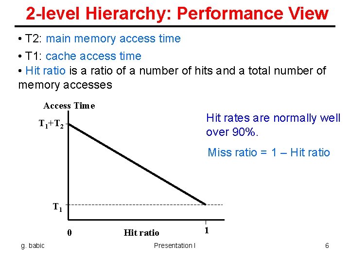
2 -level Hierarchy: Performance View • T 2: main memory access time • T 1: cache access time • Hit ratio is a ratio of a number of hits and a total number of memory accesses Access Time Hit rates are normally well over 90%. T 1+T 2 Miss ratio = 1 – Hit ratio T 1 0 g. babic Hit ratio Presentation I 1 6

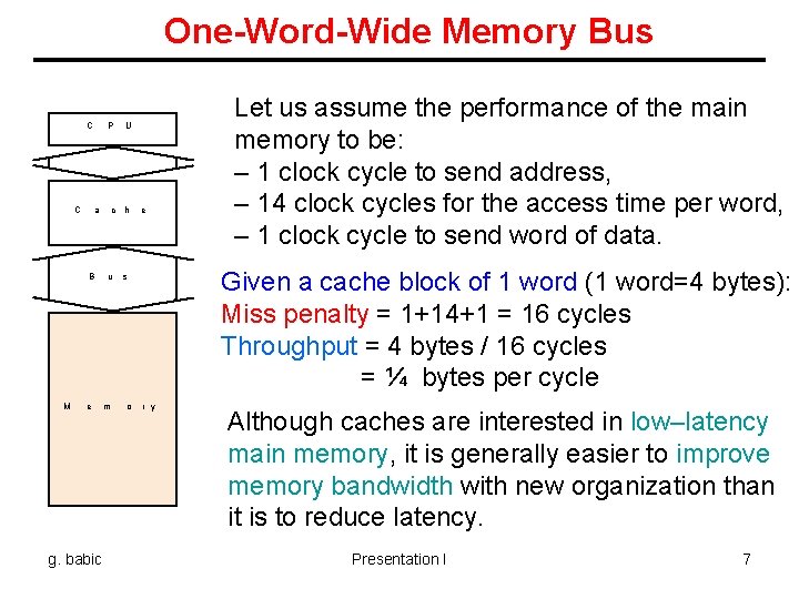
One-Word-Wide Memory Bus C C P a B M e g. babic U c h u s m o e Let us assume the performance of the main memory to be: – 1 clock cycle to send address, – 14 clock cycles for the access time per word, – 1 clock cycle to send word of data. Given a cache block of 1 word (1 word=4 bytes): Miss penalty = 1+14+1 = 16 cycles Throughput = 4 bytes / 16 cycles = ¼ bytes per cycle r y Although caches are interested in low–latency main memory, it is generally easier to improve memory bandwidth with new organization than it is to reduce latency. Presentation I 7

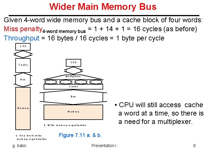
Wider Main Memory Bus Given 4 -word wide memory bus and a cache block of four words: Miss penalty 4 -word memory bus = 1 + 14 + 1 = 16 cycles (as before) Throughput = 16 bytes / 16 cycles = 1 byte per cycle CPU C a ch e M u l t ip le x o r B us C a ch e B us • CPU will still access cache a word at a time, so there is a need for a multiplexer. M e m o ry M em ory b. W id e m o r y o r g a n i z a ti o n a. O n e - w o rd - w id e m o r y o r g a n i z a ti o n g. babic Figure 7. 11 a. & b. Presentation I 8

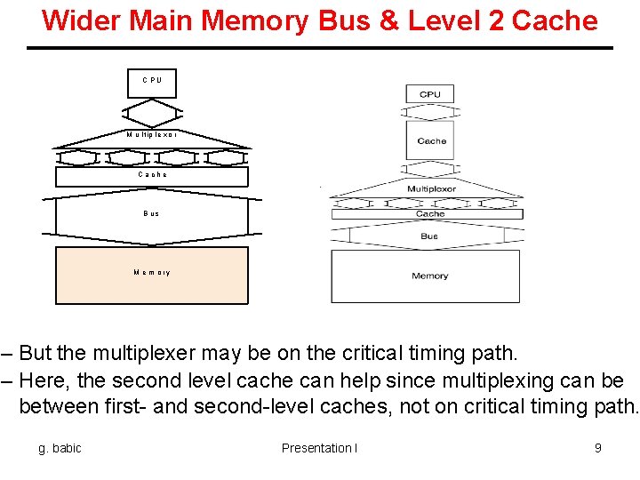
Wider Main Memory Bus & Level 2 Cache CPU M u l t ip l e x o r C a ch e B us M em ory – But the multiplexer may be on the critical timing path. – Here, the second level cache can help since multiplexing can be between first- and second-level caches, not on critical timing path. g. babic Presentation I 9

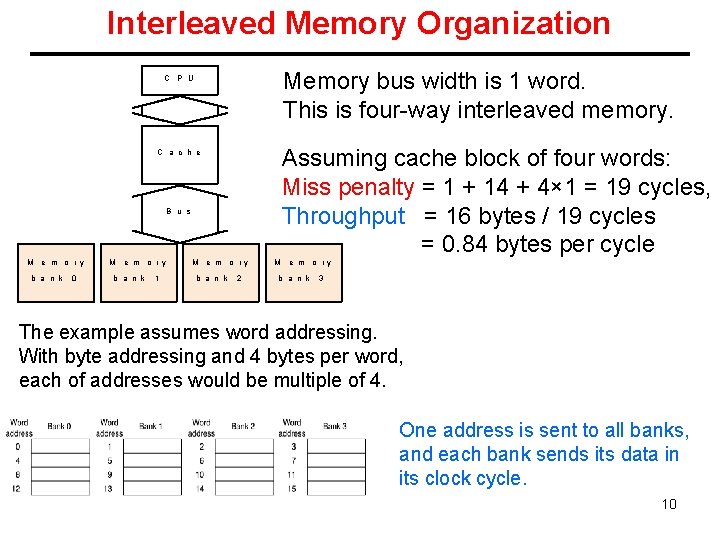
Interleaved Memory Organization Memory bus width is 1 word. This is four-way interleaved memory. C P U Assuming cache block of four words: Miss penalty = 1 + 14 + 4× 1 = 19 cycles, Throughput = 16 bytes / 19 cycles = 0. 84 bytes per cycle C a c h e B u s M e m o ry b a n k 0 M e m o r y b a n k 1 M e m o ry b a n k 2 M e m o ry b a n k 3 The example assumes word addressing. With byte addressing and 4 bytes per word, each of addresses would be multiple of 4. One address is sent to all banks, and each bank sends its data in its clock cycle. 10

Basics of Cache Design Elements of cache design: • cache size, i. e. a number of entries, • block (line) size, i. e. a number of data elements per entry, • a number of caches, • mapping functions: block placement and block identification, • replacement algorithm, • write policy. g. babic Presentation I 11

Cache Size and Block Size • Cache size << main memory size; • Cache size small enough to: – minimize cost, – speed up access (less gates to address the cache), and – keep cache on chip; • Cache size large enough: – Minimize average access time Average access time = hit time + (1 – hit rate) × Miss penalty • Smaller blocks do not take advantage of spatial locality; • Larger blocks reduce the number of blocks – replacement overhead; g. babic Presentation I 12

Number of Caches • Increased logic density => on-chip cache – internal cache: level 1 (L 1), – external or internal cache: level 2 (L 2); • Unified cache – balances the load between instruction and data fetches, – only one cache needs to be designed and implemented; • Split caches (data cache and instruction cache) – pipelined, parallel architectures; g. babic Presentation I 13

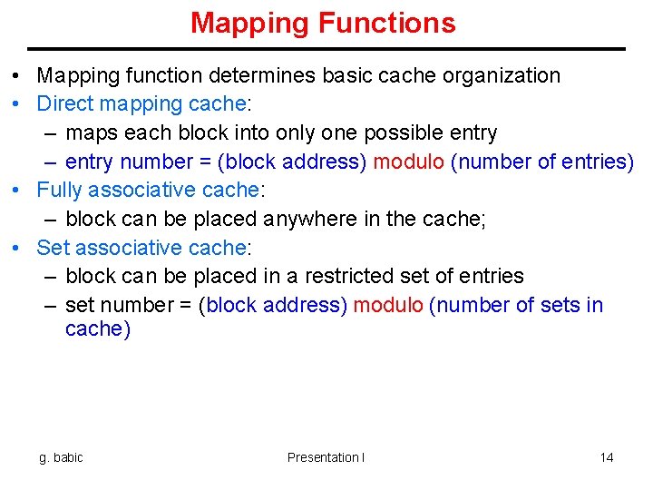
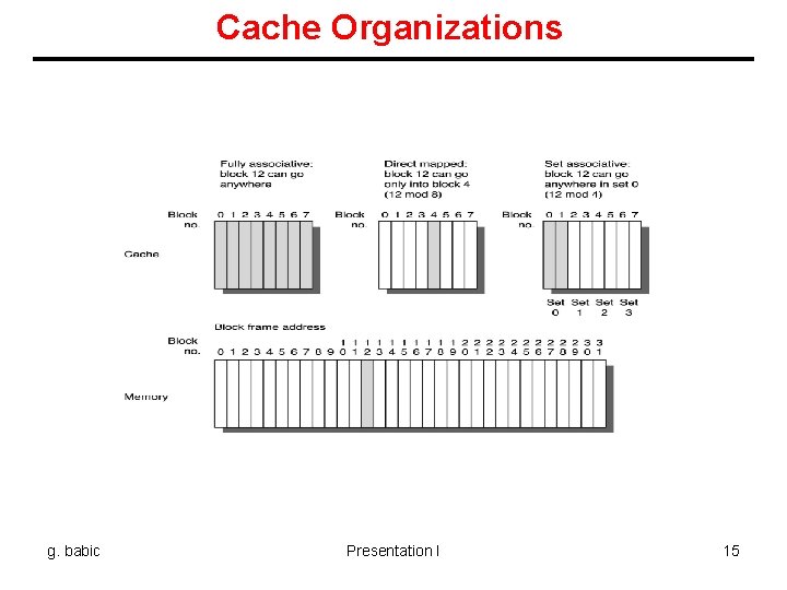
Mapping Functions • Mapping function determines basic cache organization • Direct mapping cache: – maps each block into only one possible entry – entry number = (block address) modulo (number of entries) • Fully associative cache: – block can be placed anywhere in the cache; • Set associative cache: – block can be placed in a restricted set of entries – set number = (block address) modulo (number of sets in cache) g. babic Presentation I 14

Cache Organizations g. babic Presentation I 15

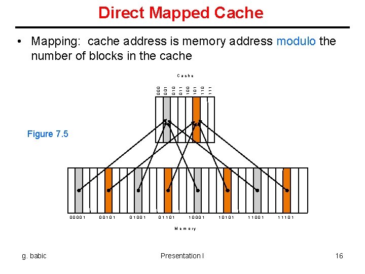
Direct Mapped Cache • Mapping: cache address is memory address modulo the number of blocks in the cache 111 1 10 1 01 010 001 000 C ache Figure 7. 5 00001 00101 01001 01101 10001 10101 11001 11101 M e m o ry g. babic Presentation I 16

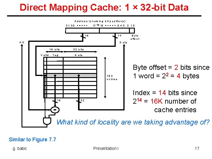
Direct Mapping Cache: 1 × 32 -bit Data A d d r e s s ( s h o w i n g b it p o s i tio n s ) 31 30 17 16 15 5 4 3 2 1 0 16 14 H it B y te o ffs e t D a ta V a li d 1 6 b i ts 3 2 b it s Tag D a ta 16 K e n tr ie s 16 Byte offset = 2 bits since 1 word = 22 = 4 bytes Index = 14 bits since 214 = 16 K number of cache entries 32 What kind of locality are we taking advantage of? Similar to Figure 7. 7 g. babic Presentation I 17

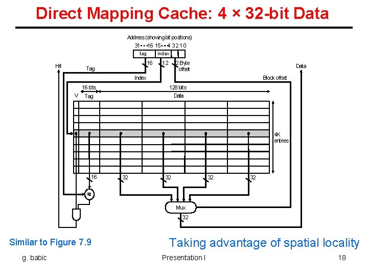
Direct Mapping Cache: 4 × 32 -bit Data Address (showing bit positions) 31 16 15 4 32 10 tag Hit index 16 Tag 12 2 Byte offset Data Index V Block offset 16 bits 128 bits Tag Data 4 K entries 16 32 32 Mux 32 Similar to Figure 7. 9 g. babic Taking advantage of spatial locality Presentation I 18

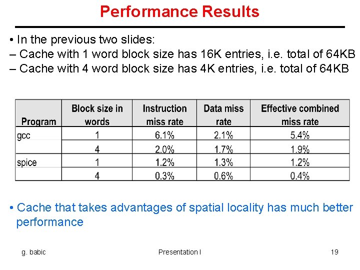
Performance Results • In the previous two slides: – Cache with 1 word block size has 16 K entries, i. e. total of 64 KB – Cache with 4 word block size has 4 K entries, i. e. total of 64 KB • Cache that takes advantages of spatial locality has much better performance g. babic Presentation I 19

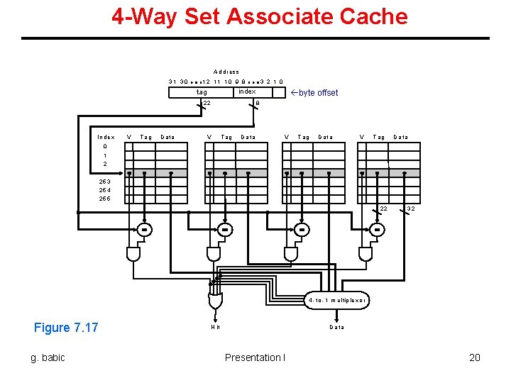
4 -Way Set Associate Cache A ddress 31 30 12 11 10 9 8 tag V Tag D a ta byte offset 8 22 In d e x 3 2 1 0 index V Tag D a ta V T ag D a ta 0 1 2 25 3 25 4 25 5 22 32 4 - to - 1 m u ltip le xo r Figure 7. 17 g. babic H it D a ta Presentation I 20

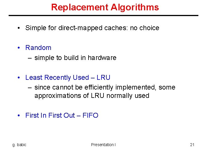
Replacement Algorithms • Simple for direct-mapped caches: no choice • Random – simple to build in hardware • Least Recently Used – LRU – since cannot be efficiently implemented, some approximations of LRU normally used • First In First Out – FIFO g. babic Presentation I 21

Write Policy • Write is more complex than read: – write and tag comparison can not proceed simultaneously, – only a portion of the block has to be updated; • Write policies: – write through – write to the cache and memory; – write back – write only to the cache, and write in memory when block is replaced (dirty bit); Write through is usually found today only in the first-level data caches backed by level 2 cache that uses write back. • Write hits: – write-through: replace data in cache and memory – write-back: write the data only into the cache and write-back into the memory later • Write misses: – read the entire block into the cache, then write the word g. babic Presentation I 22

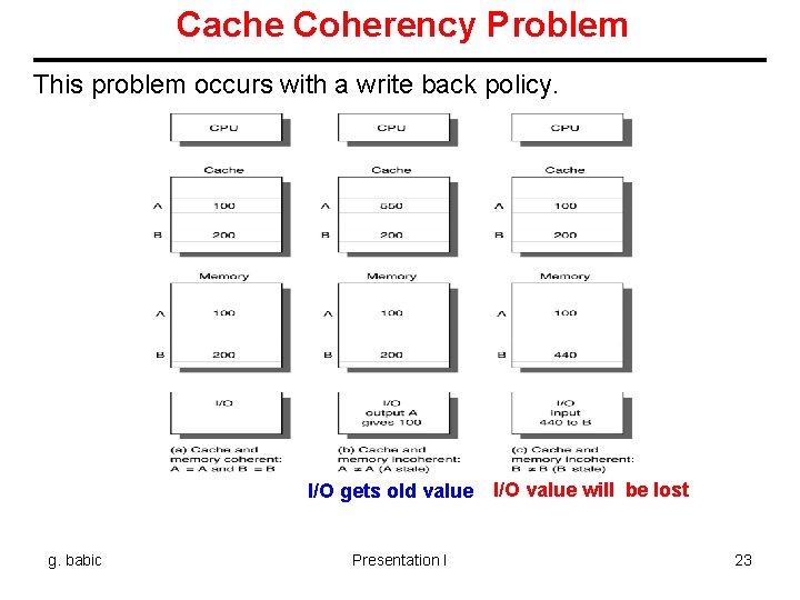
Cache Coherency Problem This problem occurs with a write back policy. I/O gets old value I/O value will be lost g. babic Presentation I 23

Solutions to Cache Coherency Problem • If write through were used, then memory would have an up-todate copy of the information, and there would be no stale-data issue for output. When write back used, the stale-data for output is not critical. • For input, the software solution is to guarantee that no blocks of the I/O buffer designated for input are in cache. Thus, the operating system always inputs to memory (pages) marked as non-cacheable. • The hardware solution is to check the I/O addresses on input to see if they are in the cache, and if there is a match, the cache entries are invalidated to avoid stale data. • Note that the cache coherency problem applies to multiprocessors as well as I/O. g. babic Presentation I 24

Summer Quarter 2005 CSE 675. 02 Introduction to Computer Architecture The End g. babic Presentation I 25