CSE 598 AEE 597 G Spring 2006 Dynamic
- Slides: 16

CSE 598 A/EE 597 G Spring 2006 Dynamic Offset Cancellation Technique Kyoung. Tae Kang, Kyusun Choi Mixed Signal Chip LAB. Kyoung Tae Kang

Motivation • The input offset voltage is the serious drawback in high precision device • Offset Voltage in CMOS is larger when compared to BJT and Bi. CMOS • For example, - For Opamp with Av=100, 0. 1 m. V input offset voltage leads 10 m. V error at output. - For series Opamp with Av=100, 0. 1 m. V input offset voltage of each stage leads the serious malfunction of chip • The effective DC offset cancellation technique is needed in CMOS Mixed Signal Chip LAB. Kyoung Tae Kang

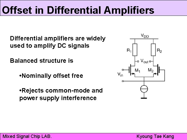
Offset in Differential Amplifiers Differential amplifiers are widely used to amplify DC signals Balanced structure is • Nominally offset free • Rejects common-mode and power supply interference Mixed Signal Chip LAB. Kyoung Tae Kang

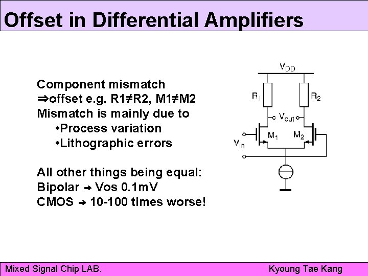
Offset in Differential Amplifiers Component mismatch ⇒offset e. g. R 1≠R 2, M 1≠M 2 Mismatch is mainly due to • Process variation • Lithographic errors All other things being equal: Bipolar ⇒ Vos 0. 1 m. V CMOS ⇒ 10 -100 times worse! Mixed Signal Chip LAB. Kyoung Tae Kang

Offset Compensation • Offsets exist all of the CMOS design • But we can reduce offset “enough” by – 1. Using “large” devices and good layout – 2. Trimming – 3. Dynamic offset-cancellation (DOC) techniques • But residual offset & frequency drawback still remain Mixed Signal Chip LAB. Kyoung Tae Kang

DOC Versus Trimming Advantage • reduction of offset and 1/f noise • excellent long term stability • no additional costs for testing Disadvantage • reduced bandwidth • increased circuit complexity • aliasing & intermodulation issues Mixed Signal Chip LAB. Kyoung Tae Kang

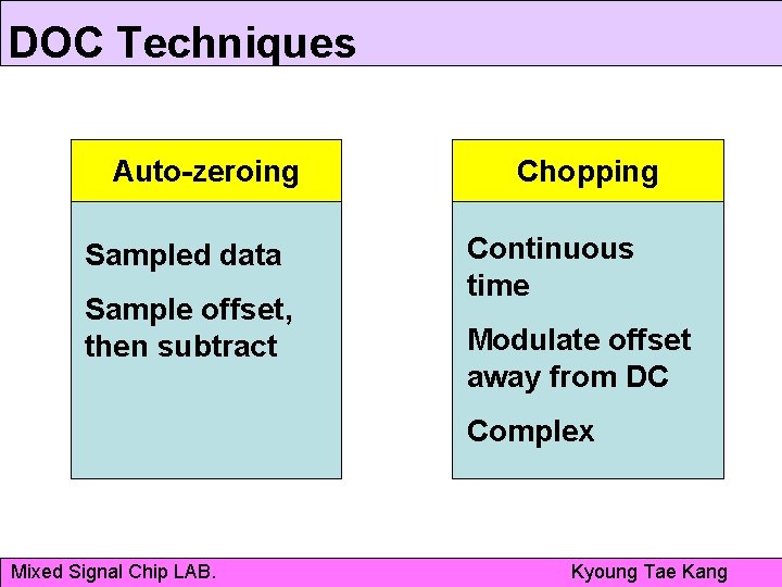
DOC Techniques Auto-zeroing Sampled data Sample offset, then subtract Chopping Continuous time Modulate offset away from DC Complex Mixed Signal Chip LAB. Kyoung Tae Kang

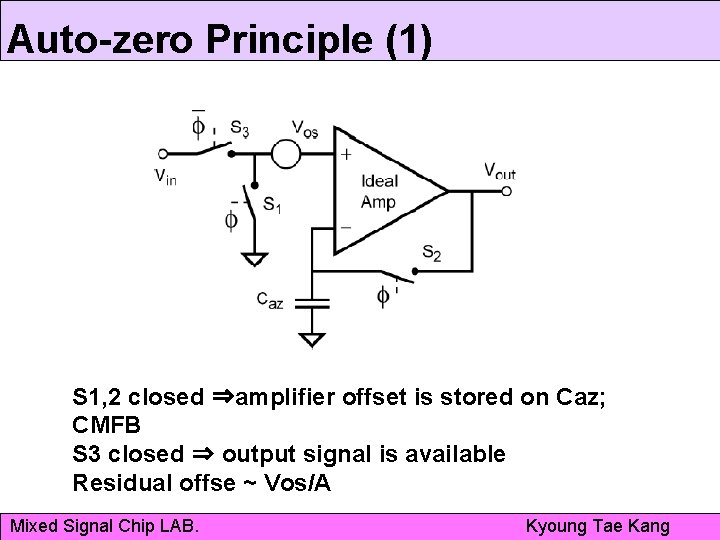
Auto-zero Principle (1) S 1, 2 closed ⇒amplifier offset is stored on Caz; CMFB S 3 closed ⇒ output signal is available Residual offse ~ Vos/A Mixed Signal Chip LAB. Kyoung Tae Kang

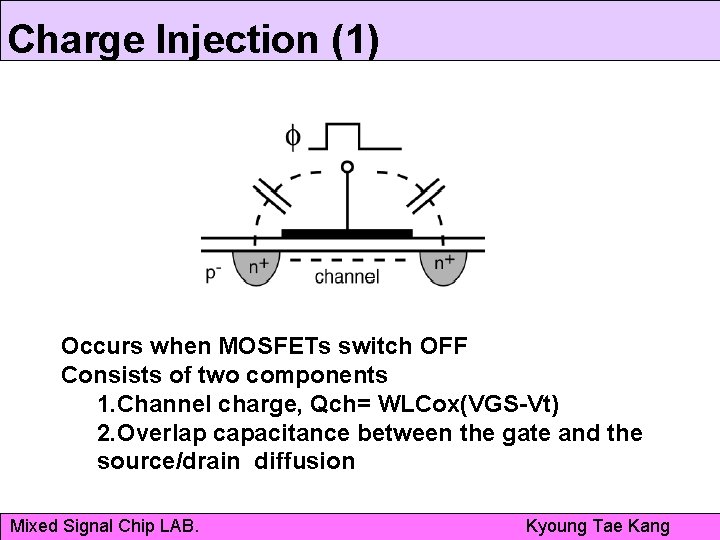
Charge Injection (1) Occurs when MOSFETs switch OFF Consists of two components 1. Channel charge, Qch= WLCox(VGS-Vt) 2. Overlap capacitance between the gate and the source/drain diffusion Mixed Signal Chip LAB. Kyoung Tae Kang

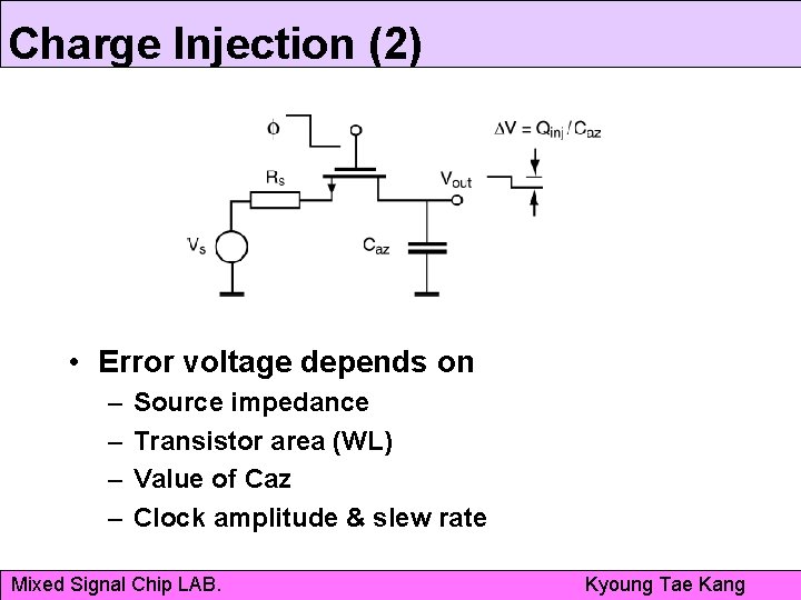
Charge Injection (2) • Error voltage depends on – – Source impedance Transistor area (WL) Value of Caz Clock amplitude & slew rate Mixed Signal Chip LAB. Kyoung Tae Kang

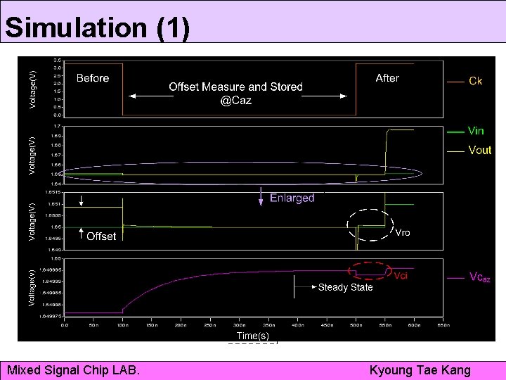
Simulation (1) Mixed Signal Chip LAB. Kyoung Tae Kang

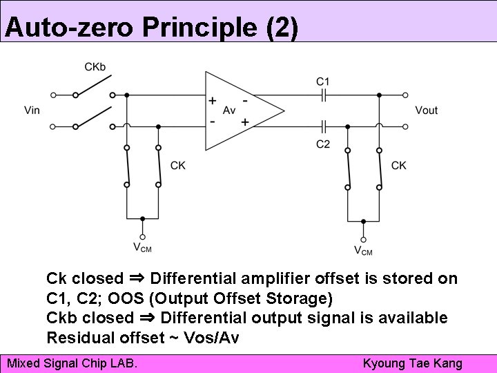
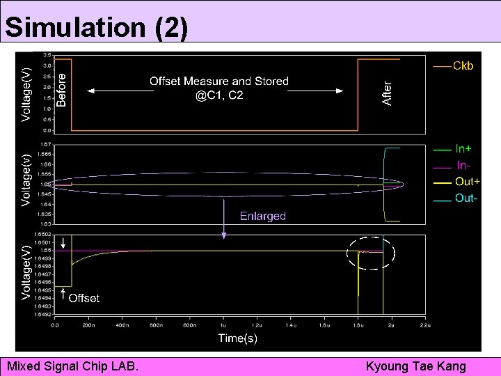
Auto-zero Principle (2) Ck closed ⇒ Differential amplifier offset is stored on C 1, C 2; OOS (Output Offset Storage) Ckb closed ⇒ Differential output signal is available Residual offset ~ Vos/Av Mixed Signal Chip LAB. Kyoung Tae Kang

Simulation (2) Mixed Signal Chip LAB. Kyoung Tae Kang

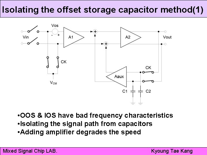
Isolating the offset storage capacitor method(1) • OOS & IOS have bad frequency characteristics • Isolating the signal path from capacitors • Adding amplifier degrades the speed Mixed Signal Chip LAB. Kyoung Tae Kang

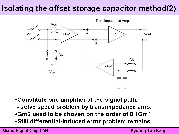
Isolating the offset storage capacitor method(2) • Constitute one amplifier at the signal path. - solve speed problem by transimpedance amp. • Gm 2 used to be chosen on the order of 0. 1 Gm 1 • Still differential-induced error problem remains Mixed Signal Chip LAB. Kyoung Tae Kang

Design Consideration • Design differential amp & single amp without offset • Using OOS cancellation technique • Choose the suitable capacitor for the application • Reset period; numbers of KHz • Storage time must be longer than the settling time of storage capacitor • As high Av is, as low residual offset is • But, as high Av is, as high the effect of clock mismatch is • Considering the effect of offset when determine the resolution of Flash ADC Mixed Signal Chip LAB. Kyoung Tae Kang