CSE 560 Computer Systems Architecture Technology Survey What
![Technology Trends 1 million 1 thousand 1 hundred [Bresniker et al. , 2015] Technology Trends 1 million 1 thousand 1 hundred [Bresniker et al. , 2015]](https://slidetodoc.com/presentation_image_h/0079937a73161ec3759e79bdc2edb98b/image-12.jpg)




- Slides: 40

CSE 560 Computer Systems Architecture Technology

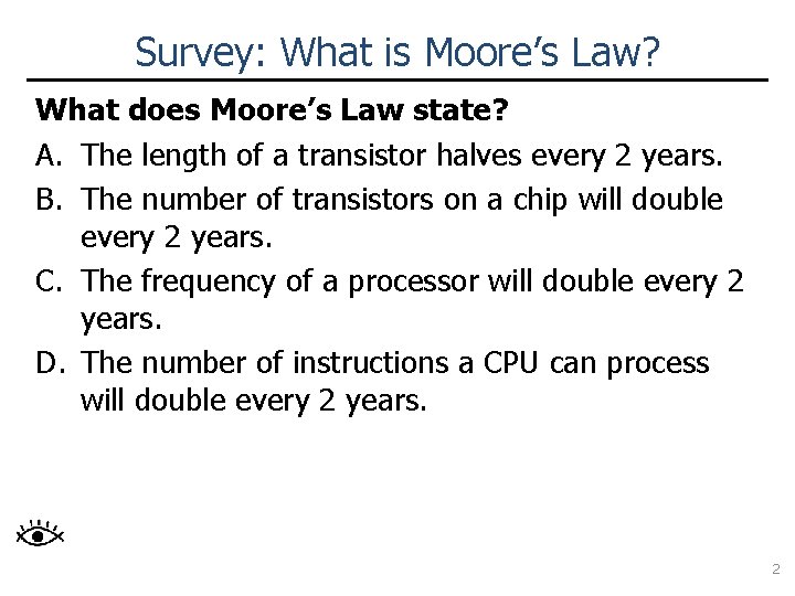
Survey: What is Moore’s Law? What does Moore’s Law state? A. The length of a transistor halves every 2 years. B. The number of transistors on a chip will double every 2 years. C. The frequency of a processor will double every 2 years. D. The number of instructions a CPU can process will double every 2 years. 2

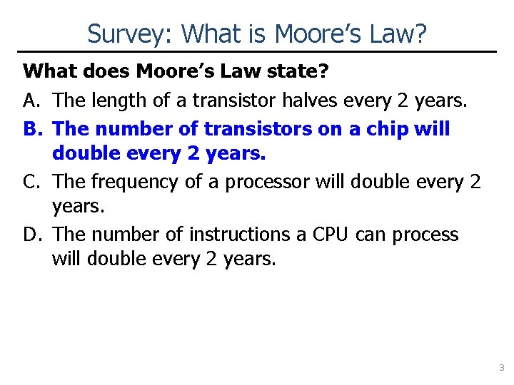
Survey: What is Moore’s Law? What does Moore’s Law state? A. The length of a transistor halves every 2 years. B. The number of transistors on a chip will double every 2 years. C. The frequency of a processor will double every 2 years. D. The number of instructions a CPU can process will double every 2 years. 3

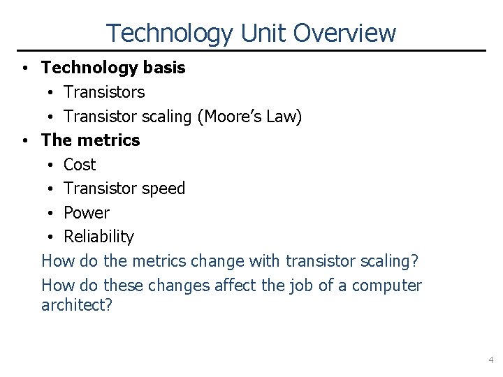
Technology Unit Overview • Technology basis • Transistor scaling (Moore’s Law) • The metrics • Cost • Transistor speed • Power • Reliability How do the metrics change with transistor scaling? How do these changes affect the job of a computer architect? 4

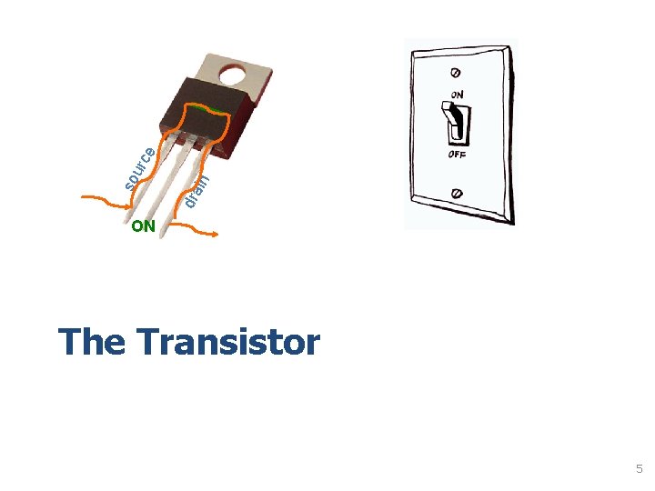
dra i n e so urc ON The Transistor 5

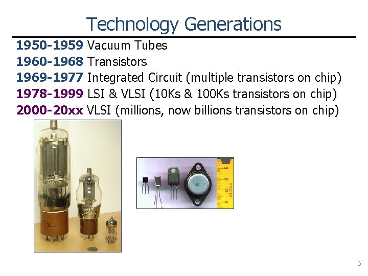
Technology Generations 1950 -1959 Vacuum Tubes 1960 -1968 Transistors 1969 -1977 Integrated Circuit (multiple transistors on chip) 1978 -1999 LSI & VLSI (10 Ks & 100 Ks transistors on chip) 2000 -20 xx VLSI (millions, now billions transistors on chip) 6

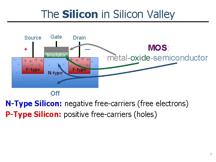
The Silicon in Silicon Valley Source + Gate Insulator Drain — + + - - - + + + P-type N-type - - - + + - + + + P-type MOS: metal-oxide-semiconductor Off N-Type Silicon: negative free-carriers (free electrons) P-Type Silicon: positive free-carriers (holes) 7

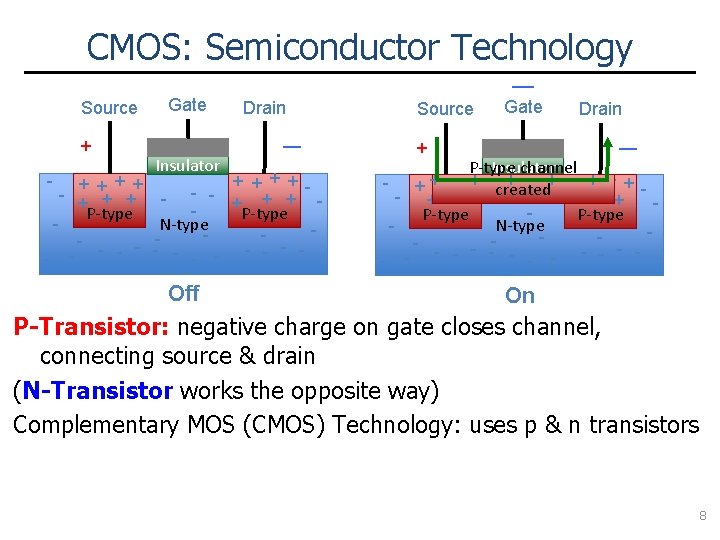
CMOS: Semiconductor Technology Source + Gate Insulator Drain — — Source Gate + Drain — + + - + + + P-type N-type - - - Insulator P-type channel + + + - + + created+ + + - - P-type N-type - - - Off On - + + + P-type P-Transistor: negative charge on gate closes channel, connecting source & drain (N-Transistor works the opposite way) Complementary MOS (CMOS) Technology: uses p & n transistors 8

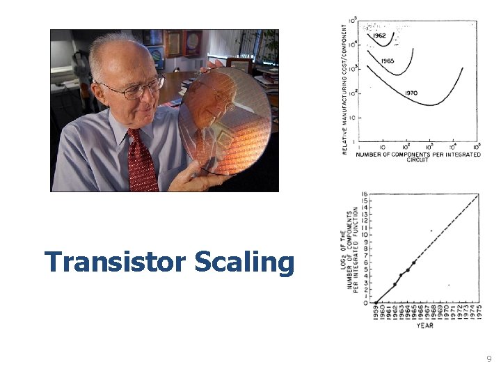
Transistor Scaling 9

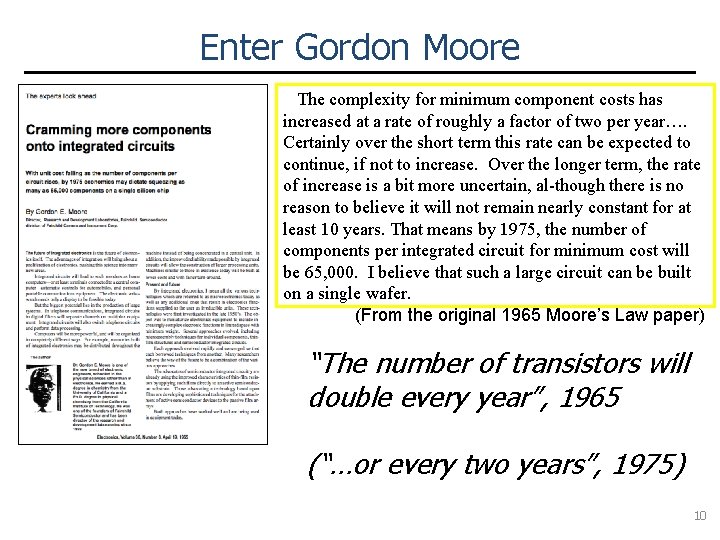
Enter Gordon Moore The complexity for minimum component costs has increased at a rate of roughly a factor of two per year…. Certainly over the short term this rate can be expected to continue, if not to increase. Over the longer term, the rate of increase is a bit more uncertain, al-though there is no reason to believe it will not remain nearly constant for at least 10 years. That means by 1975, the number of components per integrated circuit for minimum cost will be 65, 000. I believe that such a large circuit can be built on a single wafer. (From the original 1965 Moore’s Law paper) “The number of transistors will double every year”, 1965 (“…or every two years”, 1975) 10

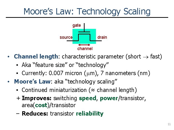
Moore’s Law: Technology Scaling gate source drain channel • Channel length: characteristic parameter (short fast) • Aka “feature size” or “technology” • Currently: 0. 007 micron (mm), 7 nanometers (nm) • Moore’s Law: aka “technology scaling” • Continued miniaturization (≈ channel length) + Improves: switching speed, power/transistor, area(cost)/transistor – Reduces: transistor reliability 11
![Technology Trends 1 million 1 thousand 1 hundred Bresniker et al 2015 Technology Trends 1 million 1 thousand 1 hundred [Bresniker et al. , 2015]](https://slidetodoc.com/presentation_image_h/0079937a73161ec3759e79bdc2edb98b/image-12.jpg)
Technology Trends 1 million 1 thousand 1 hundred [Bresniker et al. , 2015]

Cost 14

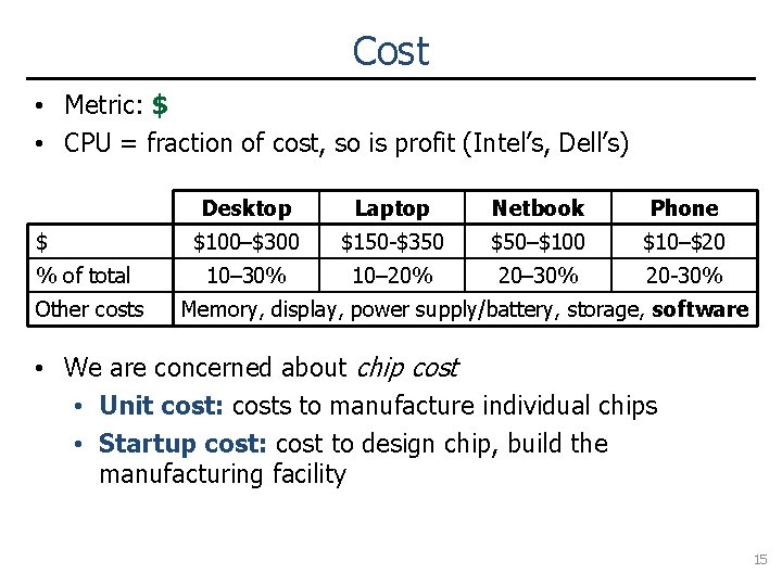
Cost • Metric: $ • CPU = fraction of cost, so is profit (Intel’s, Dell’s) $ % of total Other costs Desktop Laptop Netbook Phone $100–$300 $150 -$350 $50–$100 $10–$20 10– 30% 10– 20% 20– 30% 20 -30% Memory, display, power supply/battery, storage, software • We are concerned about chip cost • Unit cost: costs to manufacture individual chips • Startup cost: cost to design chip, build the manufacturing facility 15

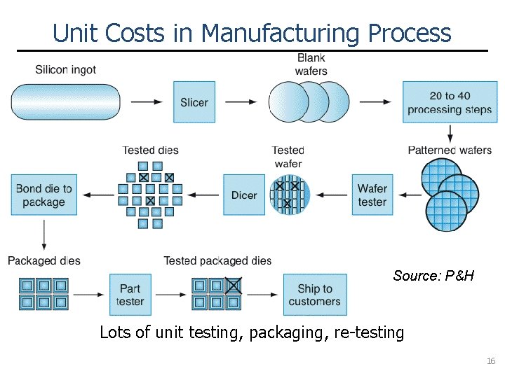
Unit Costs in Manufacturing Process Source: P&H Lots of unit testing, packaging, re-testing 16

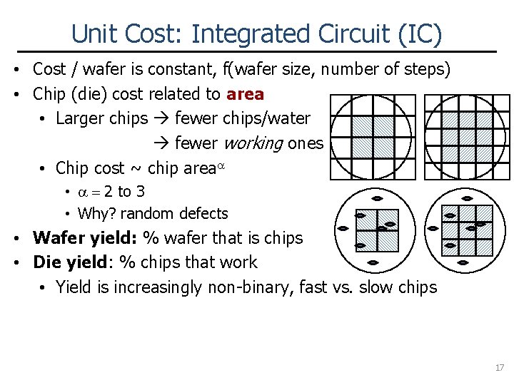
Unit Cost: Integrated Circuit (IC) • Cost / wafer is constant, f(wafer size, number of steps) • Chip (die) cost related to area • Larger chips fewer chips/water fewer working ones • Chip cost ~ chip areaa • a = 2 to 3 • Why? random defects • Wafer yield: % wafer that is chips • Die yield: % chips that work • Yield is increasingly non-binary, fast vs. slow chips 17

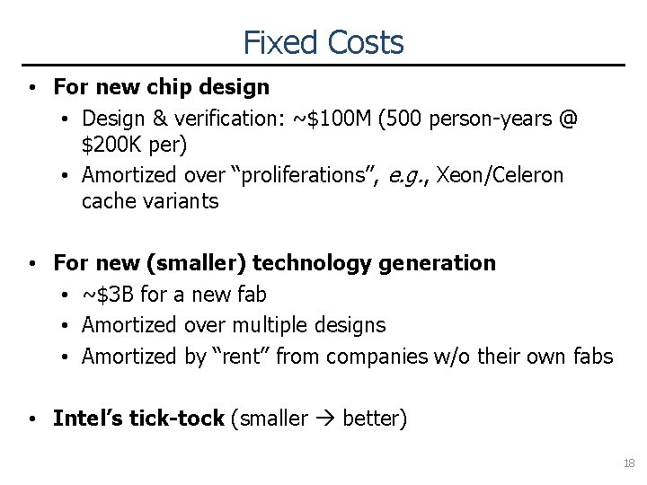
Fixed Costs • For new chip design • Design & verification: ~$100 M (500 person-years @ $200 K per) • Amortized over “proliferations”, e. g. , Xeon/Celeron cache variants • For new (smaller) technology generation • ~$3 B for a new fab • Amortized over multiple designs • Amortized by “rent” from companies w/o their own fabs • Intel’s tick-tock (smaller better) 18

Transistor Speed 21

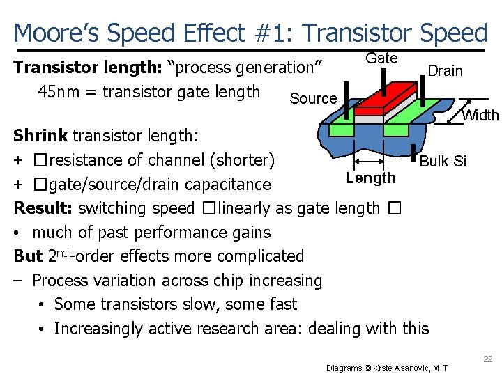
Moore’s Speed Effect #1: Transistor Speed Transistor length: “process generation” 45 nm = transistor gate length Source Gate Drain Width Shrink transistor length: + �resistance of channel (shorter) Bulk Si Length + �gate/source/drain capacitance Result: switching speed �linearly as gate length � • much of past performance gains But 2 nd-order effects more complicated – Process variation across chip increasing • Some transistors slow, some fast • Increasingly active research area: dealing with this 22 Diagrams © Krste Asanovic, MIT

Moore’s Speed Effect #2: More Transistors Linear shrink in each of 2 dimensions • 180 nm, 130 nm, 90 nm, 65 nm, 45 nm, 32 nm, 22 nm, 14 nm, 10 nm, 7 nm … • Each generation is a 1. 414 linear shrink • Results in 2 x more transistors (1. 414 x 1. 414) More transistors increased performance • Job of computer architect: figure out what to do with the ever-increasing # of transistors • Examples: caches, branch predictors, exploiting parallelism at all levels 23

Moore’s Speed Effect #3: Psychological Moore’s Curve: common interpretation of Moore’s Law • “CPU performance doubles every 18 months” • Self fulfilling prophecy: 2 x in 18 months is ~1% per week • Q: Would you add a feature that improved performance 20% if it would delay the chip 8 months? • Processors under Moore’s Curve (arrive too late) fail spectacularly • E. g. , Intel’s Itanium, Sun’s Millennium 24

Power & Energy 25

Power/Energy Increasingly Important • Battery life for mobile devices • Laptops, phones, cameras • Tolerable temperature for devices without active cooling • Power means temperature, active cooling means cost • No fan in a cell phone, no market for a hot cell phone • Electric bill for compute/data centers • Pay for power twice: once in, once out (to cool) • Environmental concerns • “Computers” account for growing fraction of energy consumption 26

Energy & Power Energy: total amount of energy stored/used • Battery life, electric bill, environmental impact Power: energy per unit time • Related to “performance” (also a “per unit time” metric) • Power impacts power supply, cooling needs (cost) • Peak power vs. average power • E. g. , camera power “spikes” when you take a picture Two sources: • Dynamic power: active switching of transistors • Static power: transistors leak even when inactive 27

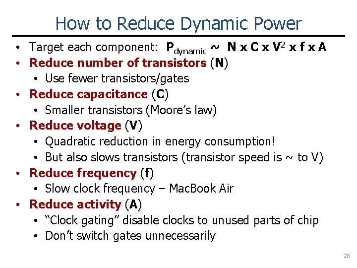
How to Reduce Dynamic Power • Target each component: Pdynamic ~ N x C x V 2 x f x A • Reduce number of transistors (N) • Use fewer transistors/gates • Reduce capacitance (C) • Smaller transistors (Moore’s law) • Reduce voltage (V) • Quadratic reduction in energy consumption! • But also slows transistors (transistor speed is ~ to V) • Reduce frequency (f) • Slow clock frequency – Mac. Book Air • Reduce activity (A) • “Clock gating” disable clocks to unused parts of chip • Don’t switch gates unnecessarily 28

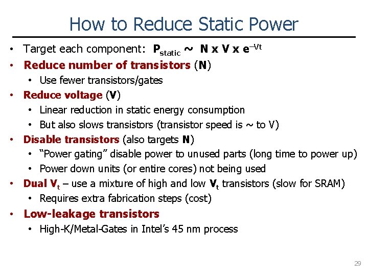
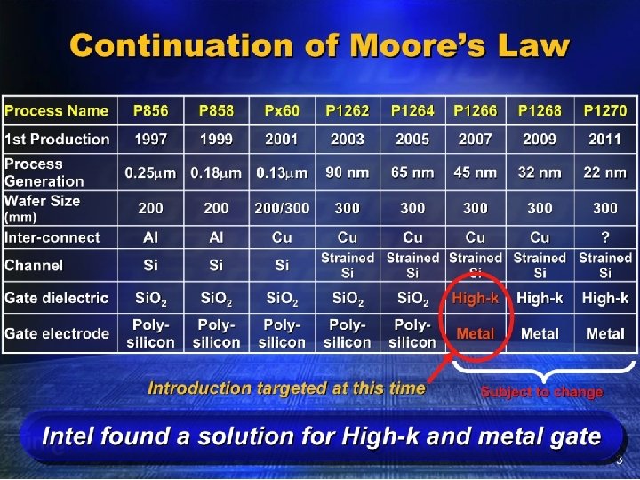
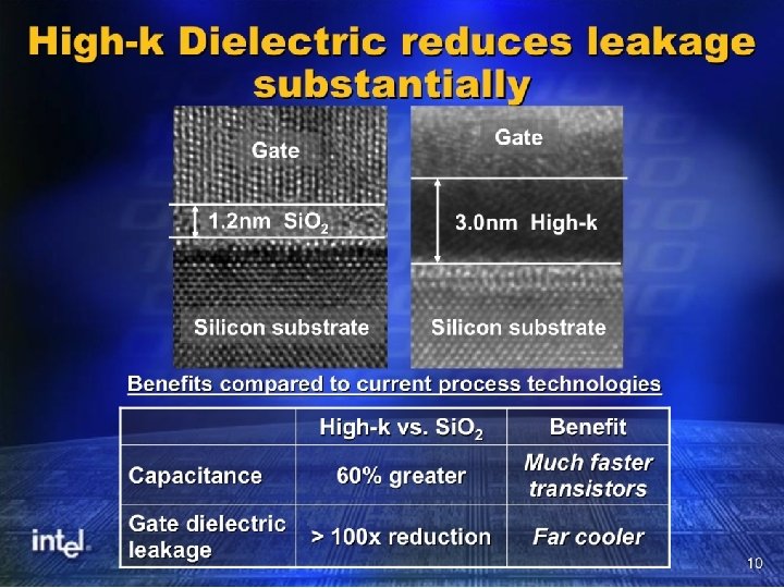
How to Reduce Static Power • Target each component: Pstatic ~ N x V x e–Vt • Reduce number of transistors (N) • Use fewer transistors/gates • Reduce voltage (V) • Linear reduction in static energy consumption • But also slows transistors (transistor speed is ~ to V) • Disable transistors (also targets N) • “Power gating” disable power to unused parts (long time to power up) • Power down units (or entire cores) not being used • Dual Vt – use a mixture of high and low Vt transistors (slow for SRAM) • Requires extra fabrication steps (cost) • Low-leakage transistors • High-K/Metal-Gates in Intel’s 45 nm process 29

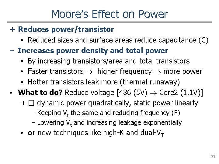
Moore’s Effect on Power + Reduces power/transistor • Reduced sizes and surface areas reduce capacitance (C) – Increases power density and total power • By increasing transistors/area and total transistors • Faster transistors higher frequency more power • Hotter transistors leak more (thermal runaway) • What to do? Reduce voltage [486 (5 V) Core 2 (1. 1 V)] + � dynamic power quadratically, static power linearly – Keeping Vt the same and reducing frequency (F) – Lowering Vt and increasing leakage exponentially • or new techniques like high-K and dual-VT 30

Continuation of Moore’s Law CSE 560 (Bracy): Technology 33

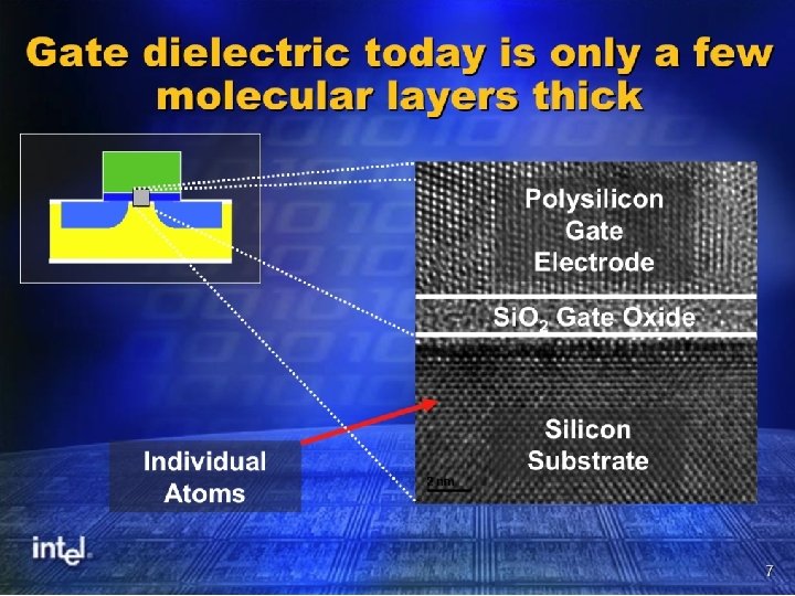
Gate dielectric today is only a few molecular layers thick CSE 560 (Bracy): Technology 34

High-k Dielectric reduces leakage substantially CSE 560 (Bracy): Technology 35

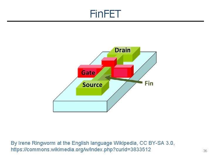
Fin. FET By Irene Ringworm at the English language Wikipedia, CC BY-SA 3. 0, https: //commons. wikimedia. org/w/index. php? curid=3833512 36

Reliability 40

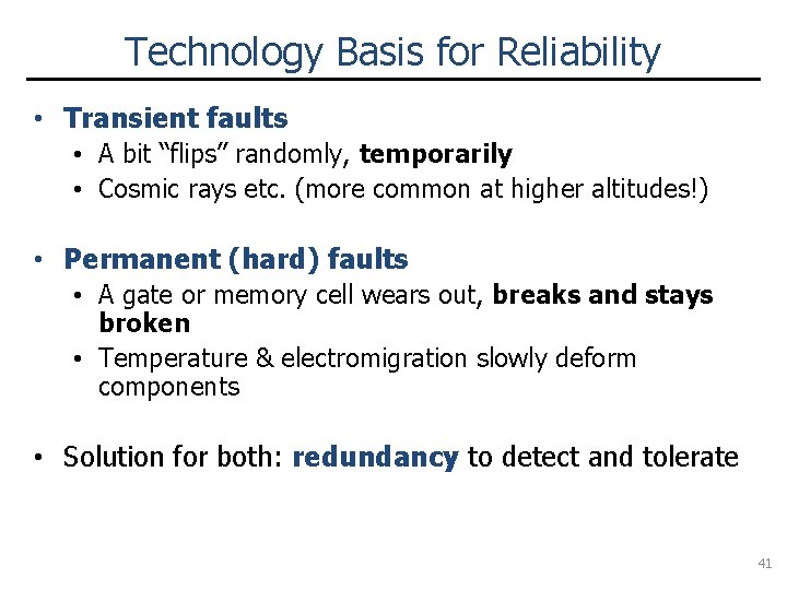
Technology Basis for Reliability • Transient faults • A bit “flips” randomly, temporarily • Cosmic rays etc. (more common at higher altitudes!) • Permanent (hard) faults • A gate or memory cell wears out, breaks and stays broken • Temperature & electromigration slowly deform components • Solution for both: redundancy to detect and tolerate 41

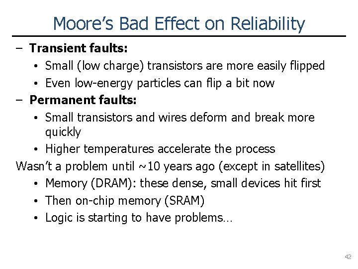
Moore’s Bad Effect on Reliability – Transient faults: • Small (low charge) transistors are more easily flipped • Even low-energy particles can flip a bit now – Permanent faults: • Small transistors and wires deform and break more quickly • Higher temperatures accelerate the process Wasn’t a problem until ~10 years ago (except in satellites) • Memory (DRAM): these dense, small devices hit first • Then on-chip memory (SRAM) • Logic is starting to have problems… 42

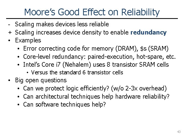
Moore’s Good Effect on Reliability - Scaling makes devices less reliable + Scaling increases device density to enable redundancy • Examples • Error correcting code for memory (DRAM), $s (SRAM) • Core-level redundancy: paired-execution, hot-spare, etc. • Intel’s Core i 7 (Nehalem) uses 8 transistor SRAM cells • Versus the standard 6 transistor cells • Big open questions • Can we protect logic efficiently? (w/o 2 -3 x overhead) • Can architectural techniques help hardware reliability? • Can software techniques help? 43

Summary 44

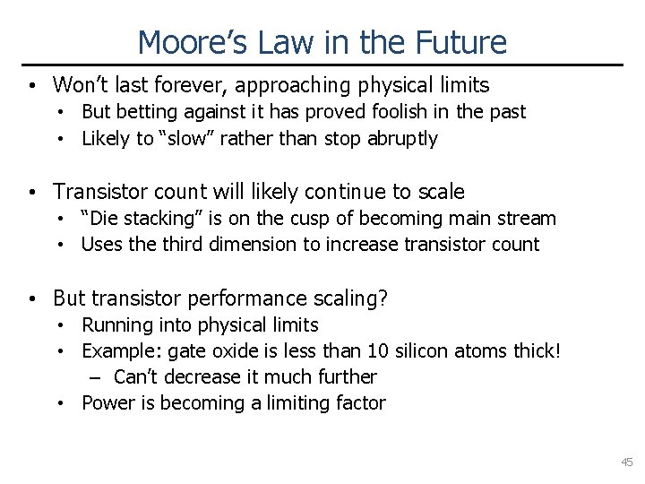
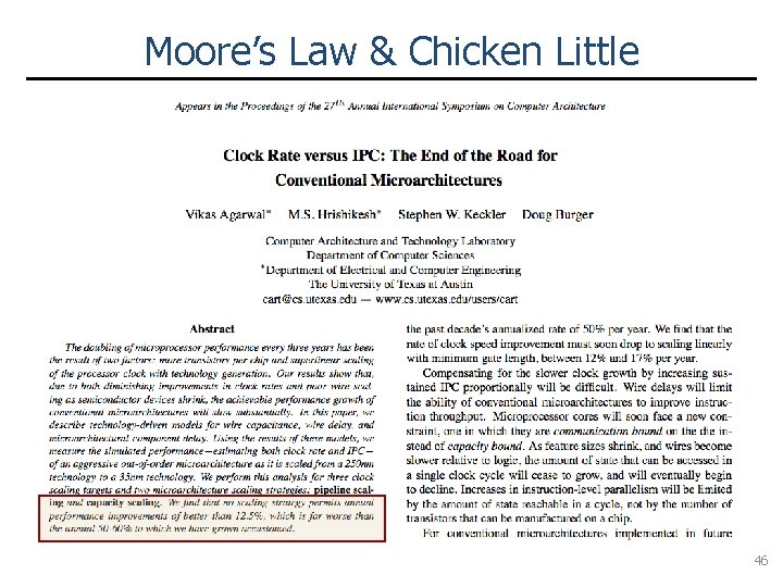
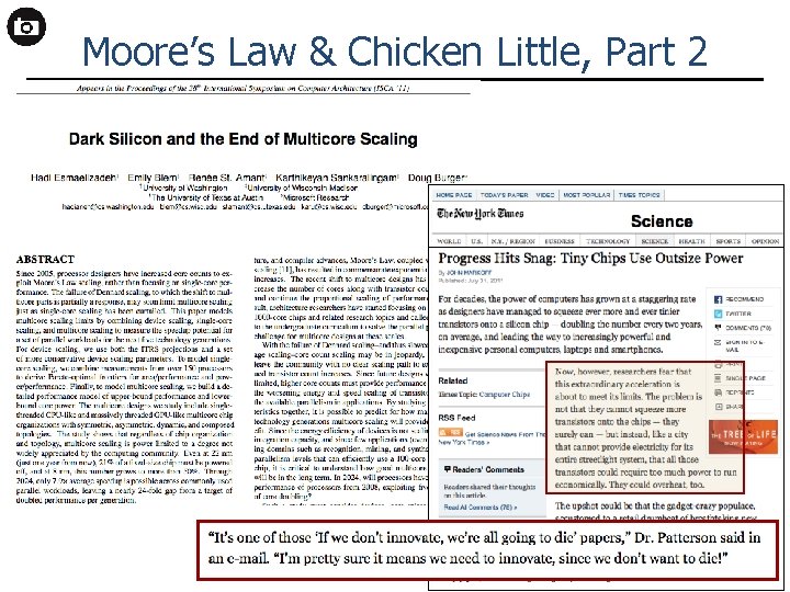
Moore’s Law in the Future • Won’t last forever, approaching physical limits • But betting against it has proved foolish in the past • Likely to “slow” rather than stop abruptly • Transistor count will likely continue to scale • “Die stacking” is on the cusp of becoming main stream • Uses the third dimension to increase transistor count • But transistor performance scaling? • Running into physical limits • Example: gate oxide is less than 10 silicon atoms thick! – Can’t decrease it much further • Power is becoming a limiting factor 45

Moore’s Law & Chicken Little 46

Moore’s Law & Chicken Little, Part 2 47

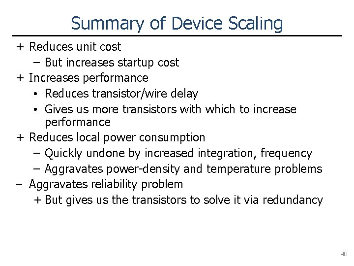
Summary of Device Scaling + Reduces unit cost – But increases startup cost + Increases performance • Reduces transistor/wire delay • Gives us more transistors with which to increase performance + Reduces local power consumption – Quickly undone by increased integration, frequency – Aggravates power-density and temperature problems – Aggravates reliability problem + But gives us the transistors to solve it via redundancy 48