CSE 140 L Lecture 3 4 bit adder
CSE 140 L Lecture 3 4 -bit adder, multiplexer, timing diagrams, propagation delays CK Cheng 1
Timing behavior • Real circuits have delays • Gate delay – time for an output of the gate to change after its input changes • We can simulate timing delays in Quartus II to see these delays 2
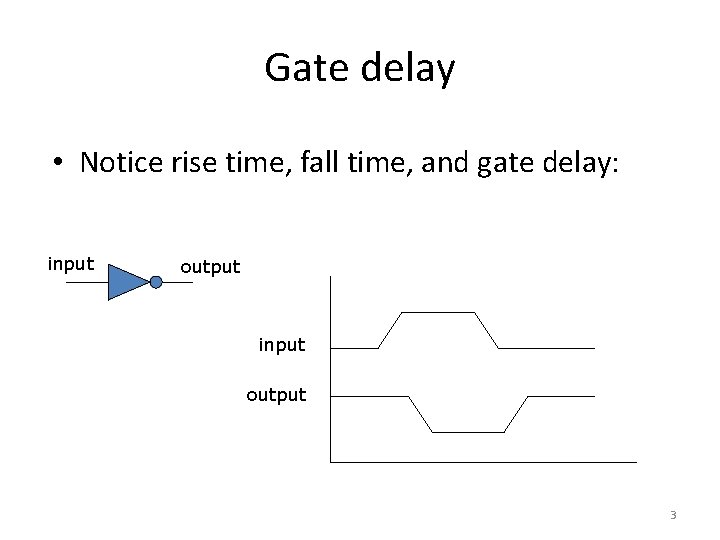
Gate delay • Notice rise time, fall time, and gate delay: input output 3
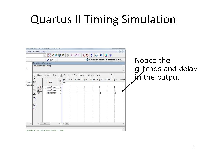
Quartus II Timing Simulation Notice the glitches and delay in the output 4
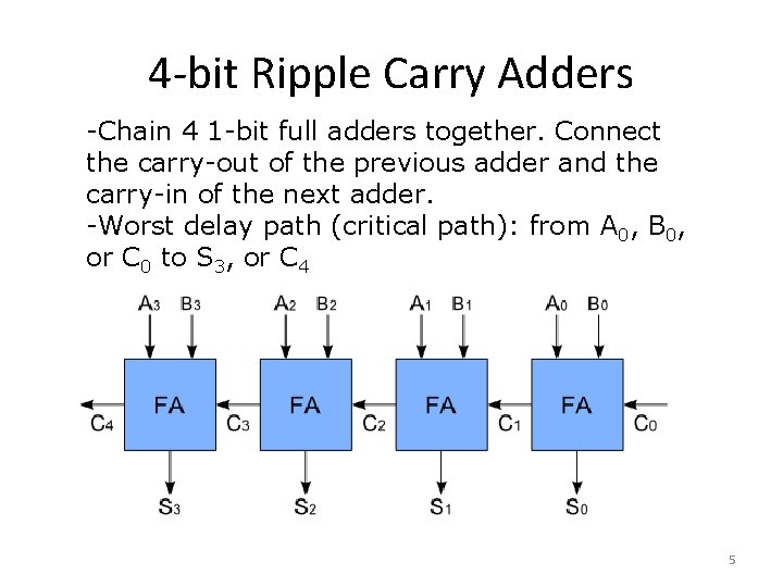
4 -bit Ripple Carry Adders -Chain 4 1 -bit full adders together. Connect the carry-out of the previous adder and the carry-in of the next adder. -Worst delay path (critical path): from A 0, B 0, or C 0 to S 3, or C 4 5
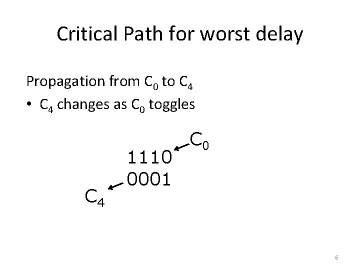
Critical Path for worst delay Propagation from C 0 to C 4 • C 4 changes as C 0 toggles C 4 1110 0001 C 0 6
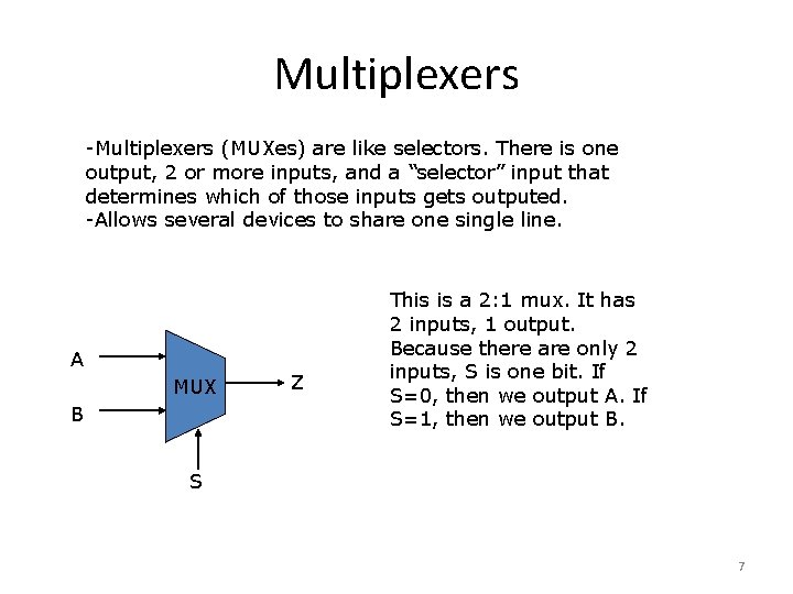
Multiplexers -Multiplexers (MUXes) are like selectors. There is one output, 2 or more inputs, and a “selector” input that determines which of those inputs gets outputed. -Allows several devices to share one single line. A MUX B Z This is a 2: 1 mux. It has 2 inputs, 1 output. Because there are only 2 inputs, S is one bit. If S=0, then we output A. If S=1, then we output B. S 7
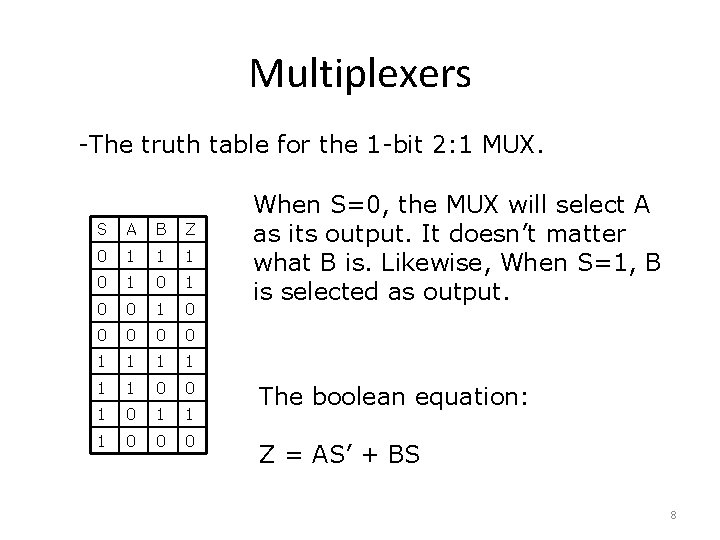
Multiplexers -The truth table for the 1 -bit 2: 1 MUX. S A B Z 0 1 1 1 0 1 0 0 0 0 0 1 1 1 0 0 0 When S=0, the MUX will select A as its output. It doesn’t matter what B is. Likewise, When S=1, B is selected as output. The boolean equation: Z = AS’ + BS 8
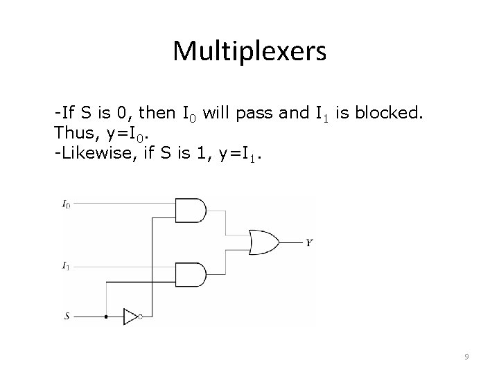
Multiplexers -If S is 0, then I 0 will pass and I 1 is blocked. Thus, y=I 0. -Likewise, if S is 1, y=I 1. 9
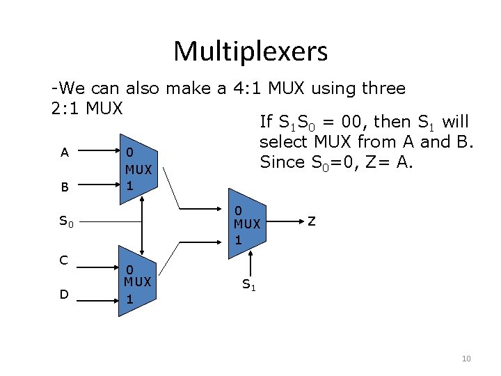
Multiplexers -We can also make a 4: 1 MUX using three 2: 1 MUX If S 1 S 0 = 00, then S 1 will select MUX from A and B. A 0 Since S 0=0, Z= A. MUX B 1 0 Z MUX 1 S 0 C D 0 MUX 1 Z S 1 10
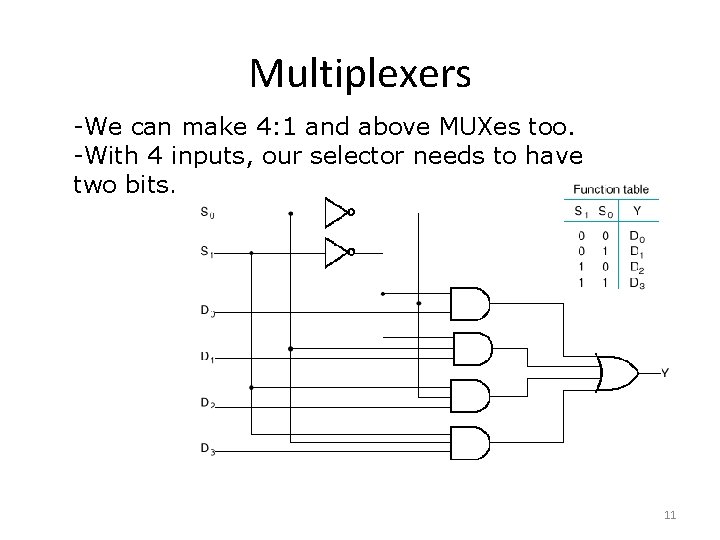
Multiplexers -We can make 4: 1 and above MUXes too. -With 4 inputs, our selector needs to have two bits. 11
Exercises Subtractors: a. Subtraction b. One’s Complement c. Two’s Complement 12
- Slides: 12