CSCOE 0447 Computer Organization Assembly Language MultiCycle Execution
CS/COE 0447 Computer Organization & Assembly Language Multi-Cycle Execution 1
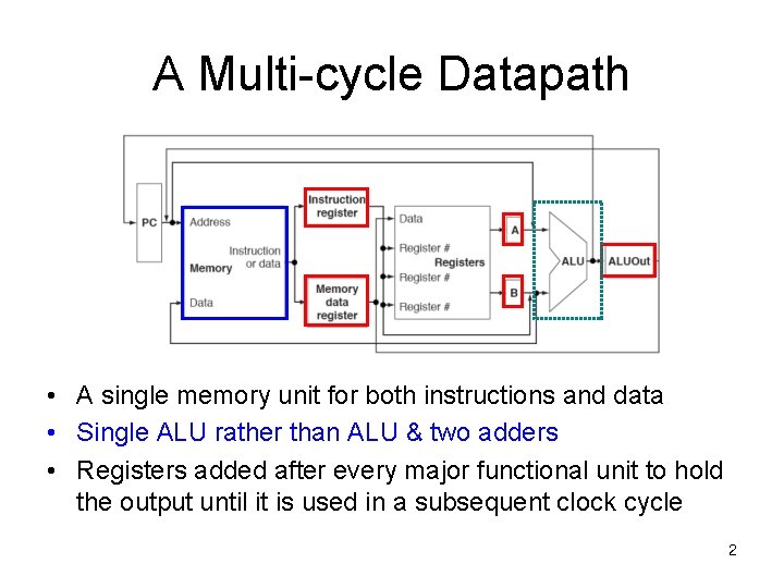
A Multi-cycle Datapath • A single memory unit for both instructions and data • Single ALU rather than ALU & two adders • Registers added after every major functional unit to hold the output until it is used in a subsequent clock cycle 2
Multi-Cycle Control What we need to cover • Adding registers after every functional unit – Need to modify the “instruction execution” slides to reflect this • Breaking instruction execution down into cycles – What can be done during the same cycle? What requires a cycle? – Need to modify the “instruction execution” slides again – Timing • Control signal values – What they are per cycle, per instruction – Finite state machine which determines signals based on instruction type + which cycle it is • Putting it all together 3
Execution: single-cycle (reminder) • add – – Fetch instruction and add 4 to PC add $t 2, $t 1, $t 0 Read two source registers $t 1 and $t 0 Add two values $t 1 + $t 0 Store result to the destination register $t 1 + $t 0 $t 2 4
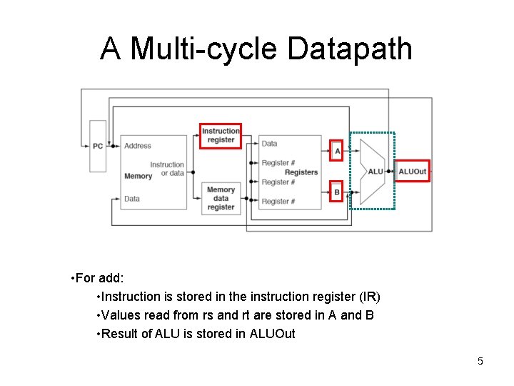
A Multi-cycle Datapath • For add: • Instruction is stored in the instruction register (IR) • Values read from rs and rt are stored in A and B • Result of ALU is stored in ALUOut 5
Execution: single-cycle (reminder) • lw (load word) – – – Fetch instruction and add 4 to PC lw $t 0, -12($t 1) Read the base register $t 1 Sign-extend the immediate offset fff 4 fffffff 4 Add two values to get address X = fffffff 4 + $t 1 Access data memory with the computed address M[X] Store the memory data to the destination register $t 0 6
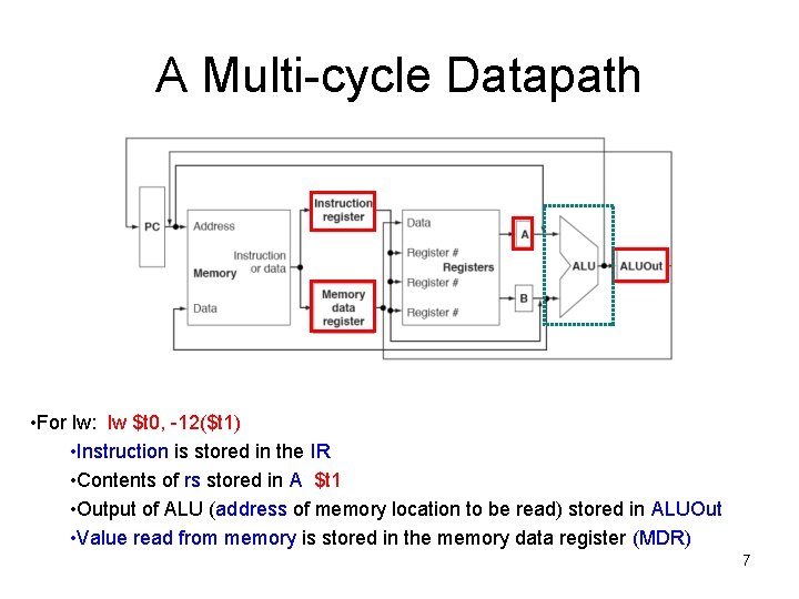
A Multi-cycle Datapath • For lw: lw $t 0, -12($t 1) • Instruction is stored in the IR • Contents of rs stored in A $t 1 • Output of ALU (address of memory location to be read) stored in ALUOut • Value read from memory is stored in the memory data register (MDR) 7
Execution: single-cycle (reminder) • sw – – – Fetch instruction and add 4 to PC sw $t 0, -4($t 1) Read the base register $t 1 Read the source register $t 0 Sign-extend the immediate offset fffc fffffffc Add two values to get address X = fffffffc + $t 1 Store the contents of the source register to the computed address $t 0 Memory[X] 8
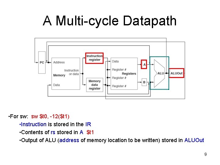
A Multi-cycle Datapath • For sw: sw $t 0, -12($t 1) • Instruction is stored in the IR • Contents of rs stored in A $t 1 • Output of ALU (address of memory location to be written) stored in ALUOut 9
Execution: single-cycle (reminder) • beq – Fetch instruction and add 4 to PC beq $t 0, $t 1, L • Assume that L is +4 instructions away – Read two source registers $t 0, $t 1 – Sign Extend the immediate, and shift it left by 2 • 0 x 0003 0 x 0000000 c – Perform the test, and update the PC if it is true • If $t 0 == $t 1, the PC = PC + 0 x 0000000 c 10
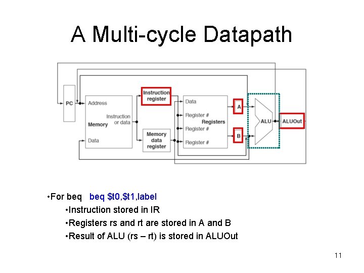
A Multi-cycle Datapath • For beq $t 0, $t 1, label • Instruction stored in IR • Registers rs and rt are stored in A and B • Result of ALU (rs – rt) is stored in ALUOut 11
Execution: single-cycle (reminder) • j – Fetch instruction and add 4 to PC – Take the 26 -bit immediate field – Shift left by 2 (to make 28 -bit immediate) – Get 4 bits from the current PC and attach to the left of the immediate – Assign the value to PC 12
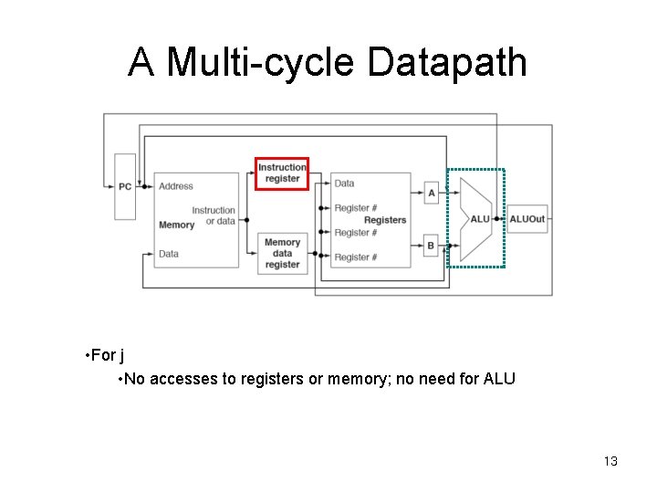
A Multi-cycle Datapath • For j • No accesses to registers or memory; no need for ALU 13
Multi-Cycle Control What we need to cover • Adding registers after every functional unit – Need to modify the “instruction execution” slides to reflect this • Breaking instruction execution down into cycles – What can be done during the same cycle? What requires a cycle? – Need to modify the “instruction execution” slides again – Timing • Control signal values – What they are per cycle, per instruction – Finite state machine which determines signals based on instruction type + which cycle it is • Putting it all together 14
Multicycle Approach • Break up the instructions into steps – each step takes one clock cycle – balance the amount of work to be done in each step/cycle so that they are about equal – restrict each cycle to use at most once each major functional unit so that such units do not have to be replicated – functional units can be shared between different cycles within one instruction 15
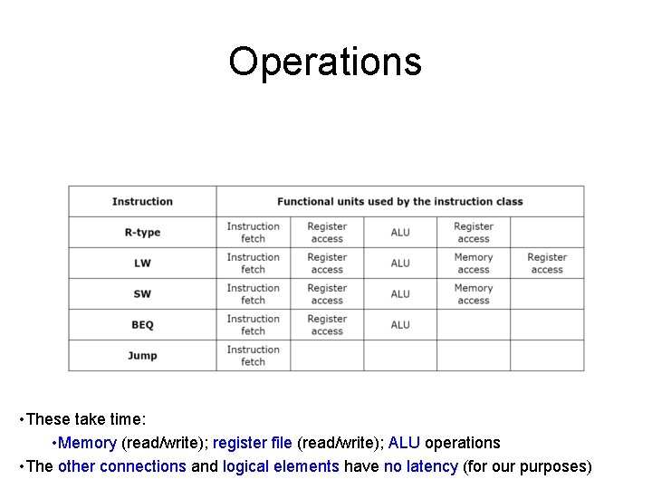
Operations • These take time: • Memory (read/write); register file (read/write); ALU operations • The other connections and logical elements have no latency (for our purposes)
Five Execution Steps • Each takes one cycle • In one cycle, there can be at most one memory access, at most one register access, and at most one ALU operation • But, you can have a memory access, an ALU op, and/or a register access, as long as there is no contention for resources • Changes to registers are made at the end of the clock cycle – PC, ALUOut, A, B, etc. save information for the next clock cycle 17
Step 1: Instruction Fetch • Access memory w/ PC to fetch instruction and store it in Instruction Register (IR) • Increment PC by 4 – We can do this because the ALU is not being used for something else this cycle 18
Step 2: Decode and Reg. Read • Read registers rs and rt – We read both of them regardless of necessity • Compute the branch address in case the instruction is a branch – We can do this because the ALU is not busy – ALUOut will keep the target address 19
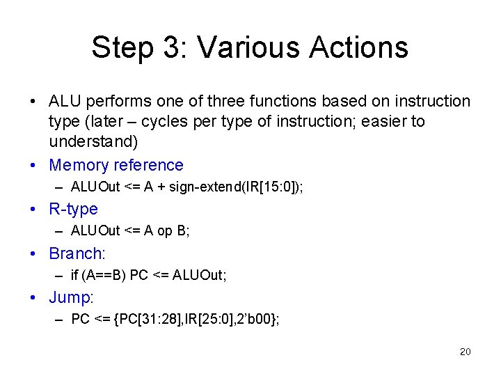
Step 3: Various Actions • ALU performs one of three functions based on instruction type (later – cycles per type of instruction; easier to understand) • Memory reference – ALUOut <= A + sign-extend(IR[15: 0]); • R-type – ALUOut <= A op B; • Branch: – if (A==B) PC <= ALUOut; • Jump: – PC <= {PC[31: 28], IR[25: 0], 2’b 00}; 20
Step 4: Memory Access… • If the instruction is memory reference – MDR <= Memory[ALUOut]; – Memory[ALUOut] <= B; // if it is a load // if it is a store • Store is complete! • If the instruction is R-type – Reg[IR[15: 11]] <= ALUOut; • Now the instruction is complete! 21
Step 5: Register Write Back • Only the lw instruction reaches this step – Reg[IR[20: 16]] <= MDR; 22
![Multicycle Execution Step (1): Instruction Fetch IR = Memory[PC]; PC = PC + 4; Multicycle Execution Step (1): Instruction Fetch IR = Memory[PC]; PC = PC + 4;](http://slidetodoc.com/presentation_image_h2/9b78d68286bd524b7091ad418ebb3a5a/image-23.jpg)
Multicycle Execution Step (1): Instruction Fetch IR = Memory[PC]; PC = PC + 4; PC + 4 4 23
![Multicycle Execution Step (2): Instruction Decode & Register Fetch A = Reg[IR[25 -21]]; (A Multicycle Execution Step (2): Instruction Decode & Register Fetch A = Reg[IR[25 -21]]; (A](http://slidetodoc.com/presentation_image_h2/9b78d68286bd524b7091ad418ebb3a5a/image-24.jpg)
Multicycle Execution Step (2): Instruction Decode & Register Fetch A = Reg[IR[25 -21]]; (A = Reg[rs]) B = Reg[IR[20 -15]]; (B = Reg[rt]) ALUOut = (PC + sign-extend(IR[15 -0]) << 2) Reg[rs] Branch Target Address PC + 4 Reg[rt] 24
![Multicycle Execution Step (3): Memory Reference Instructions ALUOut = A + sign-extend(IR[15 -0]); Reg[rs] Multicycle Execution Step (3): Memory Reference Instructions ALUOut = A + sign-extend(IR[15 -0]); Reg[rs]](http://slidetodoc.com/presentation_image_h2/9b78d68286bd524b7091ad418ebb3a5a/image-25.jpg)
Multicycle Execution Step (3): Memory Reference Instructions ALUOut = A + sign-extend(IR[15 -0]); Reg[rs] Mem. Address PC + 4 Reg[rt] 25
![Multicycle Execution Step (4): Memory Access - Write (sw) Memory[ALUOut] = B; Reg[rs] PC Multicycle Execution Step (4): Memory Access - Write (sw) Memory[ALUOut] = B; Reg[rs] PC](http://slidetodoc.com/presentation_image_h2/9b78d68286bd524b7091ad418ebb3a5a/image-26.jpg)
Multicycle Execution Step (4): Memory Access - Write (sw) Memory[ALUOut] = B; Reg[rs] PC + 4 Reg[rt] 26
![Multicycle Execution Step (4): Memory Access - Read (lw) MDR = Memory[ALUOut]; Reg[rs] Mem. Multicycle Execution Step (4): Memory Access - Read (lw) MDR = Memory[ALUOut]; Reg[rs] Mem.](http://slidetodoc.com/presentation_image_h2/9b78d68286bd524b7091ad418ebb3a5a/image-27.jpg)
Multicycle Execution Step (4): Memory Access - Read (lw) MDR = Memory[ALUOut]; Reg[rs] Mem. Address PC + 4 Mem. Data Reg[rt] 27
![Multicycle Execution Step (5): Memory Read Completion (lw) Reg[IR[20 -16]] = MDR; Reg[rs] Mem. Multicycle Execution Step (5): Memory Read Completion (lw) Reg[IR[20 -16]] = MDR; Reg[rs] Mem.](http://slidetodoc.com/presentation_image_h2/9b78d68286bd524b7091ad418ebb3a5a/image-28.jpg)
Multicycle Execution Step (5): Memory Read Completion (lw) Reg[IR[20 -16]] = MDR; Reg[rs] Mem. Address PC + 4 Mem. Data Reg[rt] 28
![Multicycle Execution Step (3): ALU Instruction (R-Type) ALUOut = A op B Reg[rs] R-Type Multicycle Execution Step (3): ALU Instruction (R-Type) ALUOut = A op B Reg[rs] R-Type](http://slidetodoc.com/presentation_image_h2/9b78d68286bd524b7091ad418ebb3a5a/image-29.jpg)
Multicycle Execution Step (3): ALU Instruction (R-Type) ALUOut = A op B Reg[rs] R-Type Result PC + 4 Reg[rt] 29
![Multicycle Execution Step (4): ALU Instruction (R-Type) Reg[IR[15: 11]] = ALUOUT Reg[rs] R-Type Result Multicycle Execution Step (4): ALU Instruction (R-Type) Reg[IR[15: 11]] = ALUOUT Reg[rs] R-Type Result](http://slidetodoc.com/presentation_image_h2/9b78d68286bd524b7091ad418ebb3a5a/image-30.jpg)
Multicycle Execution Step (4): ALU Instruction (R-Type) Reg[IR[15: 11]] = ALUOUT Reg[rs] R-Type Result PC + 4 Reg[rt] 30
![Multicycle Execution Step (3): Branch Instructions if (A == B) PC = ALUOut; Reg[rs] Multicycle Execution Step (3): Branch Instructions if (A == B) PC = ALUOut; Reg[rs]](http://slidetodoc.com/presentation_image_h2/9b78d68286bd524b7091ad418ebb3a5a/image-31.jpg)
Multicycle Execution Step (3): Branch Instructions if (A == B) PC = ALUOut; Reg[rs] Branch Target Address Reg[rt] 31
![Multicycle Execution Step (3): Jump Instruction PC = PC[31 -28] concat (IR[25 -0] << Multicycle Execution Step (3): Jump Instruction PC = PC[31 -28] concat (IR[25 -0] <<](http://slidetodoc.com/presentation_image_h2/9b78d68286bd524b7091ad418ebb3a5a/image-32.jpg)
Multicycle Execution Step (3): Jump Instruction PC = PC[31 -28] concat (IR[25 -0] << 2) Reg[rs] Branch Target Address Jump Address Reg[rt] 32
For Reference • The next 5 slides give the steps, one slide per instruction 33
![Multi-Cycle Execution: R-type • Instruction fetch – IR <= Memory[PC]; sub $t 0, $t Multi-Cycle Execution: R-type • Instruction fetch – IR <= Memory[PC]; sub $t 0, $t](http://slidetodoc.com/presentation_image_h2/9b78d68286bd524b7091ad418ebb3a5a/image-34.jpg)
Multi-Cycle Execution: R-type • Instruction fetch – IR <= Memory[PC]; sub $t 0, $t 1, $t 2 – PC <= PC + 4; • Decode instruction/register read – A <= Reg[IR[25: 21]]; rs – B <= Reg[IR[20: 16]]; rt – ALUOut <= PC + (sign-extend(IR[15: 0])<<2); • Execution – ALUOut <= A op B; op = add, sub, and, or, … • Completion – Reg[IR[15: 11]] <= ALUOut; $t 0 <= ALU result 34
![Multi-cycle Execution: lw • Instruction fetch – IR <= Memory[PC]; lw $t 0, -12($t Multi-cycle Execution: lw • Instruction fetch – IR <= Memory[PC]; lw $t 0, -12($t](http://slidetodoc.com/presentation_image_h2/9b78d68286bd524b7091ad418ebb3a5a/image-35.jpg)
Multi-cycle Execution: lw • Instruction fetch – IR <= Memory[PC]; lw $t 0, -12($t 1) – PC <= PC + 4; • Instruction Decode/register read – A <= Reg[IR[25: 21]]; rs – B <= Reg[IR[20: 16]]; – ALUOut <= PC + (sign-extend(IR[15: 0])<<2); • Execution – ALUOut <= A + sign-extend(IR[15: 0]); $t 1 + -12 (sign extended) • Memory Access – MDR <= Memory[ALUOut]; M[$t 1 + -12] • Write-back – Load: Reg[IR[20: 16]] <= MDR; $t 0 <= M[$t 1 + -12] 35
![Multi-cycle Execution: sw • Instruction fetch – IR <= Memory[PC]; sw $t 0, -12($t Multi-cycle Execution: sw • Instruction fetch – IR <= Memory[PC]; sw $t 0, -12($t](http://slidetodoc.com/presentation_image_h2/9b78d68286bd524b7091ad418ebb3a5a/image-36.jpg)
Multi-cycle Execution: sw • Instruction fetch – IR <= Memory[PC]; sw $t 0, -12($t 1) – PC <= PC + 4; • Decode/register read – A <= Reg[IR[25: 21]]; rs – B <= Reg[IR[20: 16]]; rt – ALUOut <= PC + (sign-extend(IR[15: 0])<<2); • Execution – ALUOut <= A + sign-extend(IR[15: 0]); $t 1 + -12 (sign extended) • Memory Access – Memory[ALUOut] <= B; M[$t 1 + -12] <= $t 0 36
![Multi-cycle execution: beq • Instruction fetch – IR <= Memory[PC]; beq $t 0, $t Multi-cycle execution: beq • Instruction fetch – IR <= Memory[PC]; beq $t 0, $t](http://slidetodoc.com/presentation_image_h2/9b78d68286bd524b7091ad418ebb3a5a/image-37.jpg)
Multi-cycle execution: beq • Instruction fetch – IR <= Memory[PC]; beq $t 0, $t 1, label – PC <= PC + 4; • Decode/register read – A <= Reg[IR[25: 21]]; rs – B <= Reg[IR[20: 16]]; rt – ALUOut <= PC + (sign-extend(IR[15: 0])<<2); • Execution – if (A == B) then PC <= ALUOut; • if $t 0 == $t 1 perform branch 37
![Multi-cycle execution: j • Instruction fetch – IR <= Memory[PC]; j label – PC Multi-cycle execution: j • Instruction fetch – IR <= Memory[PC]; j label – PC](http://slidetodoc.com/presentation_image_h2/9b78d68286bd524b7091ad418ebb3a5a/image-38.jpg)
Multi-cycle execution: j • Instruction fetch – IR <= Memory[PC]; j label – PC <= PC + 4; • Decode/register read – A <= Reg[IR[25: 21]]; – B <= Reg[IR[20: 16]]; – ALUOut <= PC + (sign-extend(IR[15: 0])<<2); • Execution – PC <= {PC[31: 28], IR[25: 0], ” 00”}; 38
Multi-Cycle Control What we need to cover • Adding registers after every functional unit – Need to modify the “instruction execution” slides to reflect this • Breaking instruction execution down into cycles – What can be done during the same cycle? What requires a cycle? – Need to modify the “instruction execution” slides again – Timing • Control signal values – What they are per cycle, per instruction – Finite state machine which determines signals based on instruction type + which cycle it is • Putting it all together 39
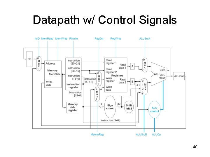
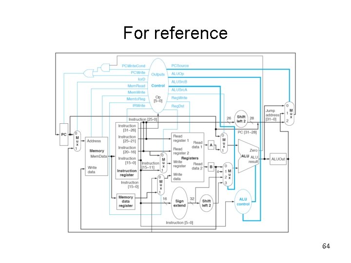
Datapath w/ Control Signals 40
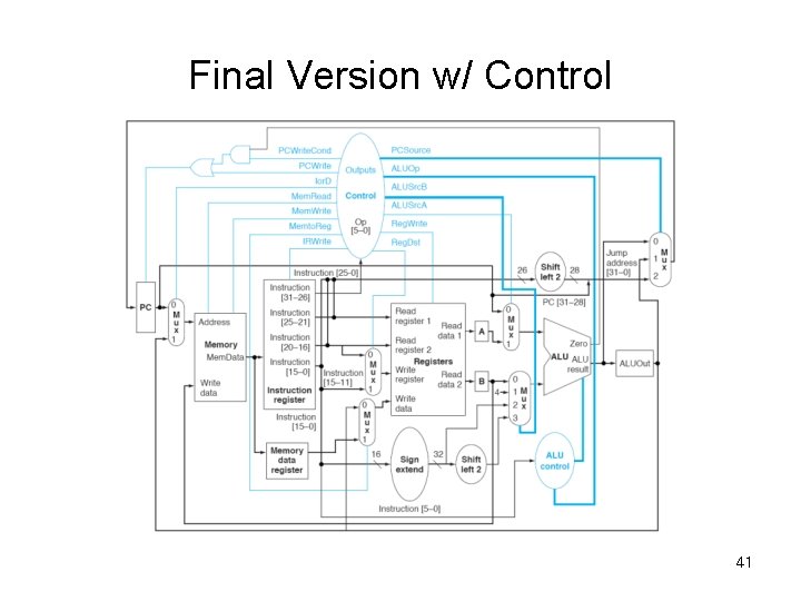
Final Version w/ Control 41
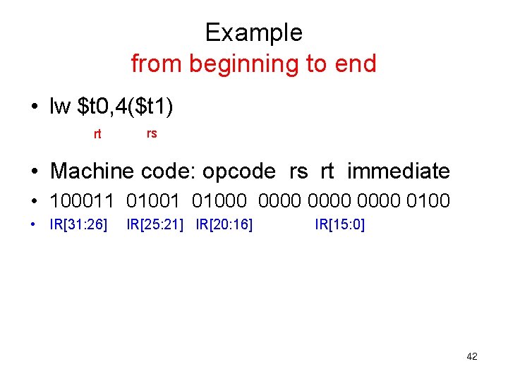
Example from beginning to end • lw $t 0, 4($t 1) rt rs • Machine code: opcode rs rt immediate • 100011 01000 0000 0100 • IR[31: 26] IR[25: 21] IR[20: 16] IR[15: 0] 42
![Multi-cycle Execution: lw • Instruction fetch – IR <= Memory[PC]; lw $t 0, -12($t Multi-cycle Execution: lw • Instruction fetch – IR <= Memory[PC]; lw $t 0, -12($t](http://slidetodoc.com/presentation_image_h2/9b78d68286bd524b7091ad418ebb3a5a/image-43.jpg)
Multi-cycle Execution: lw • Instruction fetch – IR <= Memory[PC]; lw $t 0, -12($t 1) – PC <= PC + 4; • Instruction Decode/register read – A <= Reg[IR[25: 21]]; rs – B <= Reg[IR[20: 16]]; – ALUOut <= PC + (sign-extend(IR[15: 0])<<2); • Execution – ALUOut <= A + sign-extend(IR[15: 0]); $t 1 + -12 (sign extended) • Memory Access – MDR <= Memory[ALUOut]; M[$t 1 + -12] • Write-back – Load: Reg[IR[20: 16]] <= MDR; $t 0 <= M[$t 1 + -12] 43

Example: Load (1) 00 1 1 0 0 01 00 44
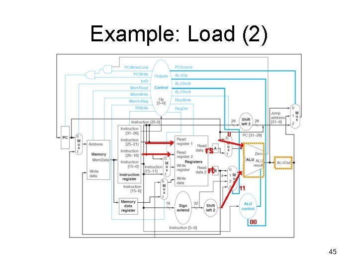
Example: Load (2) 0 rs rt 11 00 45
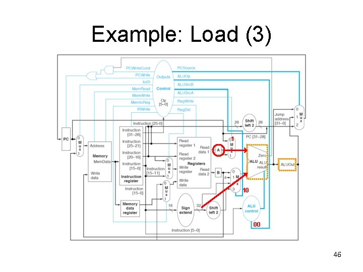
Example: Load (3) 1 10 00 46
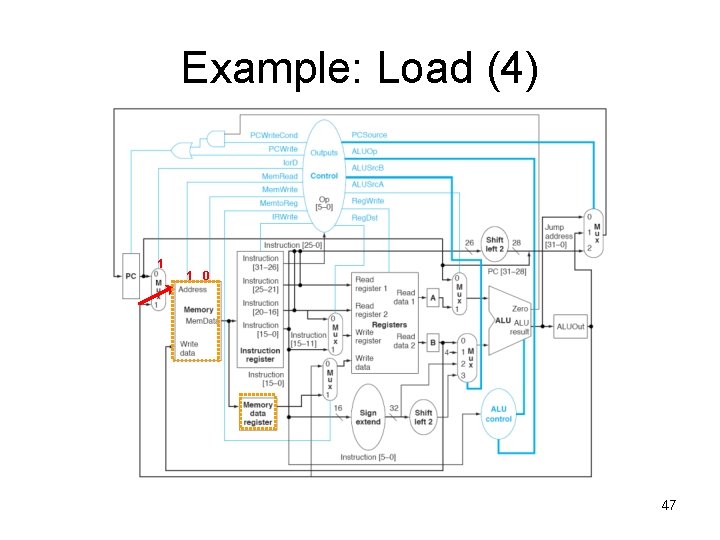
Example: Load (4) 1 1 0 47
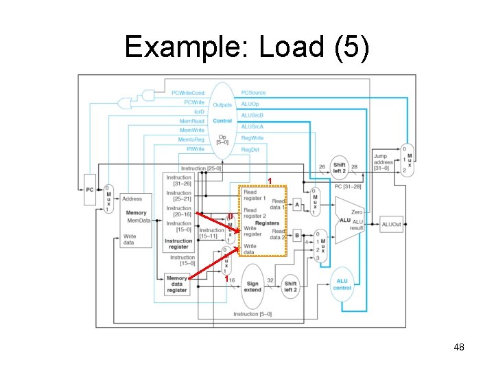
Example: Load (5) 1 0 1 48
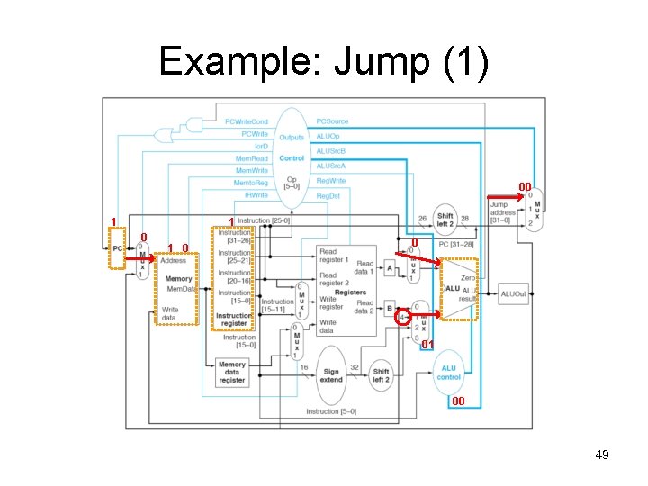
Example: Jump (1) 00 1 1 0 0 01 00 49
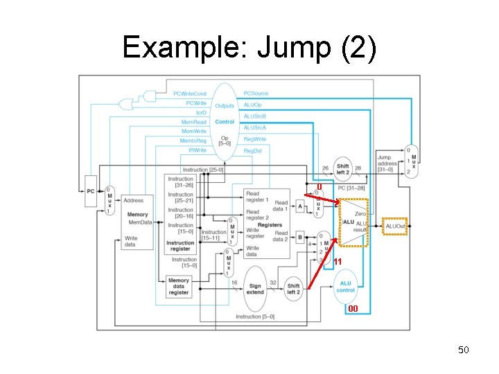
Example: Jump (2) 0 11 00 50
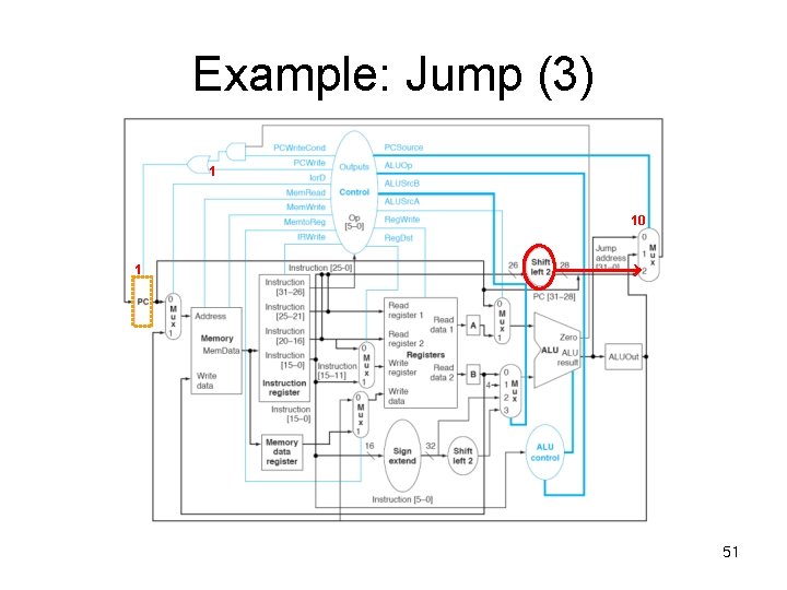
Example: Jump (3) 1 10 1 51

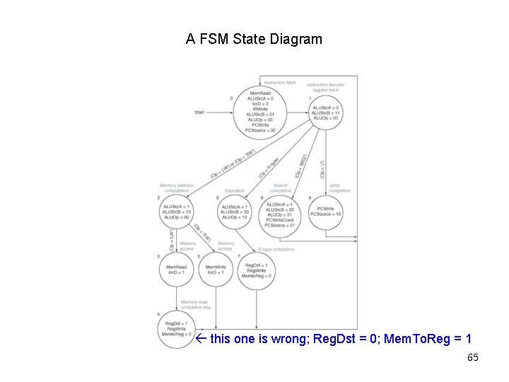
A FSM State Diagram this one is wrong; Reg. Dst = 0; Mem. To. Reg = 1 52
![Multicycle Control Step (1): Fetch IR = Memory[PC]; PC = PC + 4; 1 Multicycle Control Step (1): Fetch IR = Memory[PC]; PC = PC + 4; 1](http://slidetodoc.com/presentation_image_h2/9b78d68286bd524b7091ad418ebb3a5a/image-53.jpg)
Multicycle Control Step (1): Fetch IR = Memory[PC]; PC = PC + 4; 1 1 0 0 X 0 010 0 1 X 0 1 53
![Multicycle Control Step (2): Instruction Decode & Register Fetch A = Reg[IR[25 -21]]; (A Multicycle Control Step (2): Instruction Decode & Register Fetch A = Reg[IR[25 -21]]; (A](http://slidetodoc.com/presentation_image_h2/9b78d68286bd524b7091ad418ebb3a5a/image-54.jpg)
Multicycle Control Step (2): Instruction Decode & Register Fetch A = Reg[IR[25 -21]]; (A = Reg[rs]) B = Reg[IR[20 -15]]; (B = Reg[rt]) ALUOut = (PC + sign-extend(IR[15 -0]) << 2); 0 0 X 0 010 X 0 3 54
![Multicycle Control Step (3): Memory Reference Instructions ALUOut = A + sign-extend(IR[15 -0]); 0 Multicycle Control Step (3): Memory Reference Instructions ALUOut = A + sign-extend(IR[15 -0]); 0](http://slidetodoc.com/presentation_image_h2/9b78d68286bd524b7091ad418ebb3a5a/image-55.jpg)
Multicycle Control Step (3): Memory Reference Instructions ALUOut = A + sign-extend(IR[15 -0]); 0 0 X 1 010 X 0 2 55
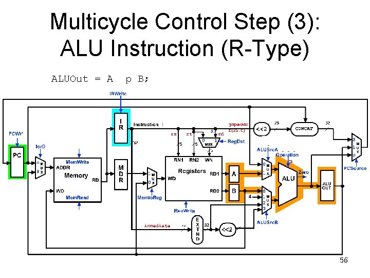
Multicycle Control Step (3): ALU Instruction (R-Type) ALUOut = A op B; 0 0 X 1 ? ? ? X 0 0 56
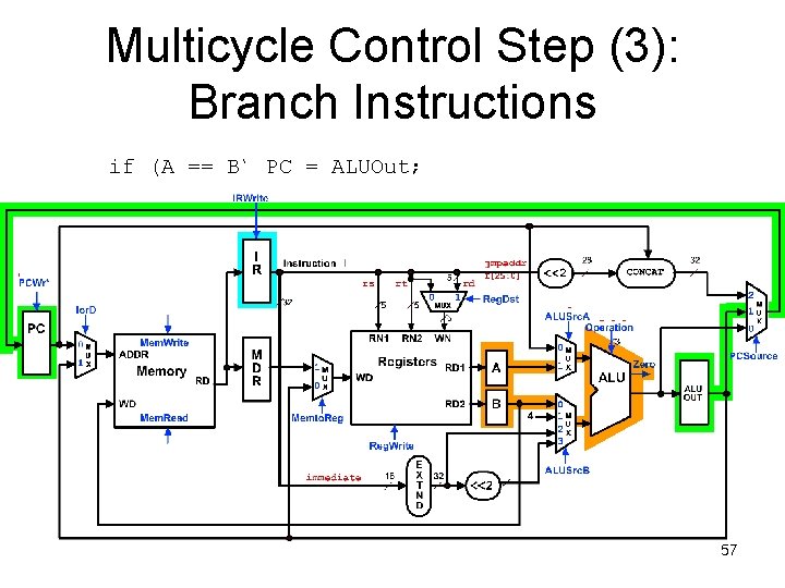
Multicycle Control Step (3): Branch Instructions if (A == B) PC = ALUOut; 0 1 if Zero=1 X 0 X 1 011 1 0 X 0 0 57
![Multicycle Execution Step (3): Jump Instruction PC = PC[21 -28] concat (IR[25 -0] << Multicycle Execution Step (3): Jump Instruction PC = PC[21 -28] concat (IR[25 -0] <<](http://slidetodoc.com/presentation_image_h2/9b78d68286bd524b7091ad418ebb3a5a/image-58.jpg)
Multicycle Execution Step (3): Jump Instruction PC = PC[21 -28] concat (IR[25 -0] << 2); 0 1 X 0 X X XXX 2 0 X 58
![Multicycle Control Step (4): Memory Access - Read (lw) MDR = Memory[ALUOut]; 0 0 Multicycle Control Step (4): Memory Access - Read (lw) MDR = Memory[ALUOut]; 0 0](http://slidetodoc.com/presentation_image_h2/9b78d68286bd524b7091ad418ebb3a5a/image-59.jpg)
Multicycle Control Step (4): Memory Access - Read (lw) MDR = Memory[ALUOut]; 0 0 1 0 X X XXX X 1 X 0 X 59
![Multicycle Execution Steps (4) Memory Access - Write (sw) Memory[ALUOut] = B; 0 0 Multicycle Execution Steps (4) Memory Access - Write (sw) Memory[ALUOut] = B; 0 0](http://slidetodoc.com/presentation_image_h2/9b78d68286bd524b7091ad418ebb3a5a/image-60.jpg)
Multicycle Execution Steps (4) Memory Access - Write (sw) Memory[ALUOut] = B; 0 0 1 1 X X XXX X 0 X 60
![Multicycle Control Step (4): ALU Instruction (R-Type) Reg[IR[15: 11]] = ALUOut; ALUOut) 0 (Reg[Rd] Multicycle Control Step (4): ALU Instruction (R-Type) Reg[IR[15: 11]] = ALUOut; ALUOut) 0 (Reg[Rd]](http://slidetodoc.com/presentation_image_h2/9b78d68286bd524b7091ad418ebb3a5a/image-61.jpg)
Multicycle Control Step (4): ALU Instruction (R-Type) Reg[IR[15: 11]] = ALUOut; ALUOut) 0 (Reg[Rd] = IRWrite I R 0 PCWr* X PC U 1 X 32 0 Memory 5 rt 5 5 0 MUX rd 1 RN 1 RD M D R 0 M U 1 X RN 2 Registers WD RD 1 RD 2 0 <<2 Reg. Dst X ALUSrc. A 1 0 M B 1 immediate Reg. Write 1 16 E X T N D 32 2 4 0 1 M U 2 X 3 0 X 3 PCSource Zero ALU X ALU OUT ALUSrc. B <<2 M 1 U XXX U 1 X A Memto. Reg 32 CONCAT Operation WN WD Mem. Read I[25: 0] 5 Mem. Write ADDR 28 jmpaddr rs Ior. D 0 M Instruction I X 61
![Multicycle Execution Steps (5) Memory Read Completion (lw) Reg[IR[20 -16]] = MDR; IRWrite I Multicycle Execution Steps (5) Memory Read Completion (lw) Reg[IR[20 -16]] = MDR; IRWrite I](http://slidetodoc.com/presentation_image_h2/9b78d68286bd524b7091ad418ebb3a5a/image-62.jpg)
Multicycle Execution Steps (5) Memory Read Completion (lw) Reg[IR[20 -16]] = MDR; IRWrite I R 0 PCWr* 0 Instruction I rs X 0 Ior. D 32 U 1 X 5 0 MUX rd 1 RN 1 RD M D R 0 M U 1 X RN 2 WD WD RD 1 RD 2 Mem. Read 0 0 immediate Reg. Write 1 16 E X T N D 32 2 XXX 4 0 1 M U 2 X 3 0 X PCSource Zero ALU X ALU OUT ALUSrc. B <<2 M 1 U 3 U 1 X A B CONCAT ALUSrc. A Operation 0 M Memto. Reg 0 X Reg. Dst WN Registers 32 <<2 I[25: 0] 5 Mem. Write ADDR Memory 5 rt 5 PC 0 M 28 jmpaddr X 62
Multi-Cycle Control What we need to cover • Adding registers after every functional unit – Need to modify the “instruction execution” slides to reflect this • Breaking instruction execution down into cycles – What can be done during the same cycle? What requires a cycle? – Need to modify the “instruction execution” slides again – Timing: Registers/memory updated at the beginning of the next clock cycle • Control signal values – What they are per cycle, per instruction – Finite state machine which determines signals based on instruction type + which cycle it is • Putting it all together 63
For reference 64
A FSM State Diagram this one is wrong; Reg. Dst = 0; Mem. To. Reg = 1 65
State Diagram, Big Picture 66
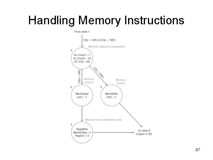
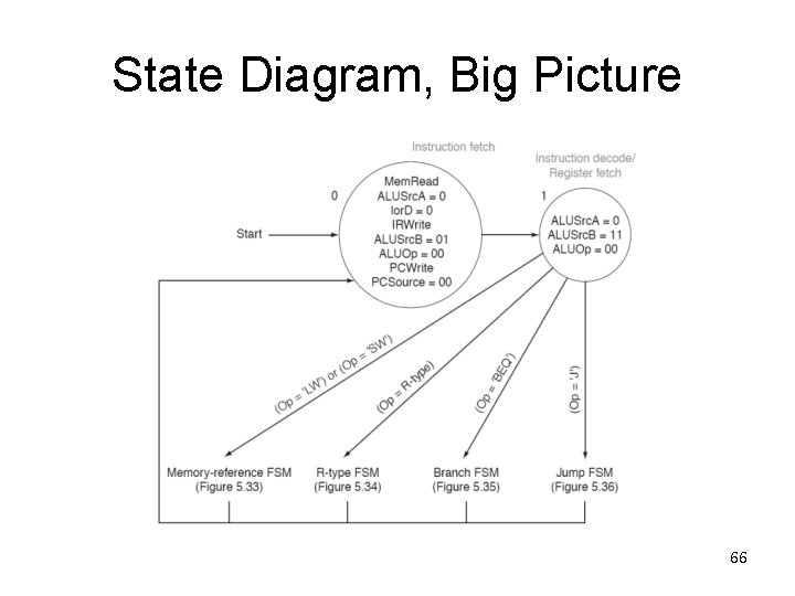
Handling Memory Instructions 67
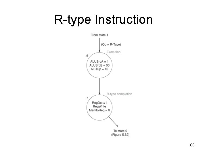
R-type Instruction 68
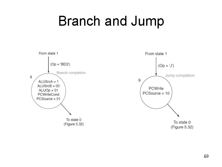
Branch and Jump 69
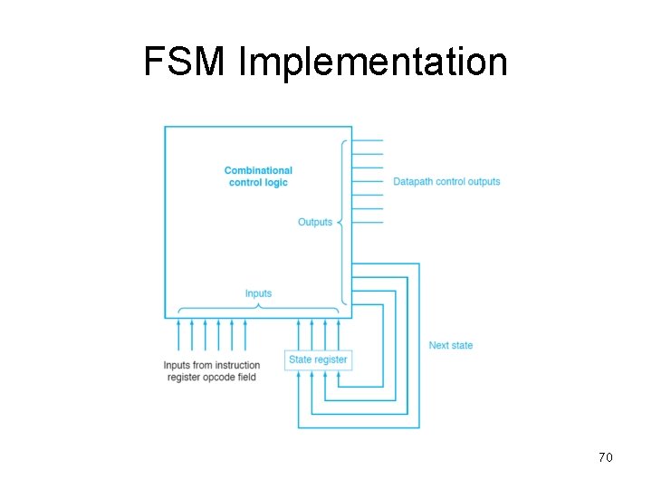
FSM Implementation 70
To Summarize… • From several building blocks, we constructed a datapath for a subset of the MIPS instruction set • First, we analyzed instructions for functional requirements • Second, we connected buildings blocks in a way to accommodate instructions • Third, we refined the datapath and added controls 71
To Summarize… • We looked at how an instruction is executed on the datapath in a pictorial way • We looked at control signals connected to functional blocks in our datapath • We analyzed how execution steps of an instruction change the control signals 72
To Summarize… • We compared a single-cycle implementation and a multi-cycle implementation of our datapath • We analyzed multi-cycle execution of instructions • We refined multi-cycle datapath • We designed multi-cycle control 73
To Summarize… • We looked at the multi-cycle control scheme in detail • Multi-cycle control can be implemented using FSM • FSM is composed of some combinational logic and memory element 74
Summary • Techniques described in this chapter to design datapaths and control are at the core of all modern computer architecture • Multicycle datapaths offer two great advantages over single-cycle – functional units can be reused within a single instruction if they are accessed in different cycles – reducing the need to replicate expensive logic – instructions with shorter execution paths can complete quicker by consuming fewer cycles • Modern computers, in fact, take the multicycle paradigm to a higher level to achieve greater instruction throughput: – pipelining (later class) where multiple instructions execute simultaneously by having cycles of different instructions overlap in the datapath – the MIPS architecture was designed to be pipelined 75
- Slides: 75