CSCE 313 Embedded System Design Introduction Instructor Jason
CSCE 313: Embedded System Design Introduction Instructor: Jason D. Bakos
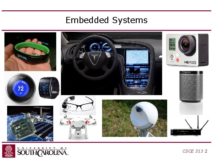
Embedded Systems CSCE 313 2
Desktop vs. Embedded CPU • General purpose (desktop and server) CPUs have a more complex structure – – • Execute up to 4 instructions per cycle Instructions executed out-of-order Big, complex caches All code runs at the same speed, since the processor finds parallelism at runtime • Exception: single core code will still only use one core, SIMD instructions often require “intrinsics” Embedded CPUs: – Generally not reprogrammable except by vendor – One or two instructions per cycle – Instructions executed in order, so instructions that depend on previous ones will “hold up the line” – Small, simple caches – Performance is dependent on code efficiency – Sometimes do not run an OS ("bare metal") or limited OS support – Tightly coupled with peripherials (system-on-chip) CSCE 313 3
Desktop vs. Embedded CPU • This class vs. 240 and 274: – Write code in C (vs. Java) – Write and debug code on a PC that runs on different processor – Write code that communicates with hardware • This class vs. 274: – Write code in C (vs. Python) – Write code that runs on bare metal – Write code containing features to improve performance – Code is more performance- and graphics-oriented CSCE 313 4
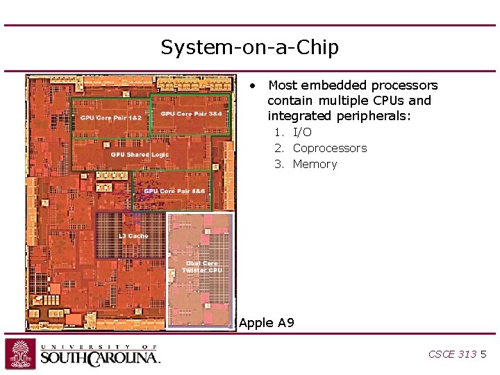
System-on-a-Chip • Most embedded processors contain multiple CPUs and integrated peripherals: 1. I/O 2. Coprocessors 3. Memory Apple A 9 CSCE 313 5
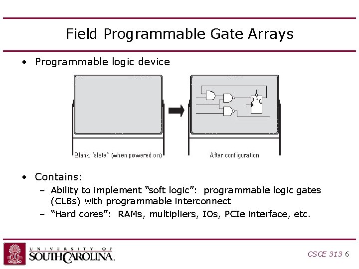
Field Programmable Gate Arrays • Programmable logic device • Contains: – Ability to implement “soft logic”: programmable logic gates (CLBs) with programmable interconnect – “Hard cores”: RAMs, multipliers, IOs, PCIe interface, etc. CSCE 313 6
Field Programmable Gate Arrays • Originally developed for “glue logic” • Now used as system-on a-programmable chip (So. PC) – – Customized “softcore” processor, Memory/cache subsystem, I/O interfaces, Off-chip memory interfaces CSCE 313 7

FPGA Lookup Table • Function generator: CSCE 313 8
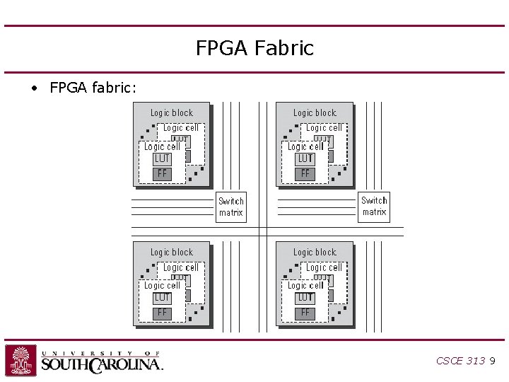
FPGA Fabric • FPGA fabric: CSCE 313 9
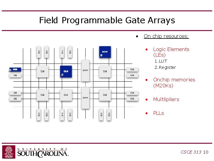
Field Programmable Gate Arrays • On chip resources: • Logic Elements (LEs) 1. LUT 2. Register • Onchip memories (M 20 Ks) • Multlipliers • PLLs CSCE 313 10

Cyclone 2 Logic Element CSCE 611 11
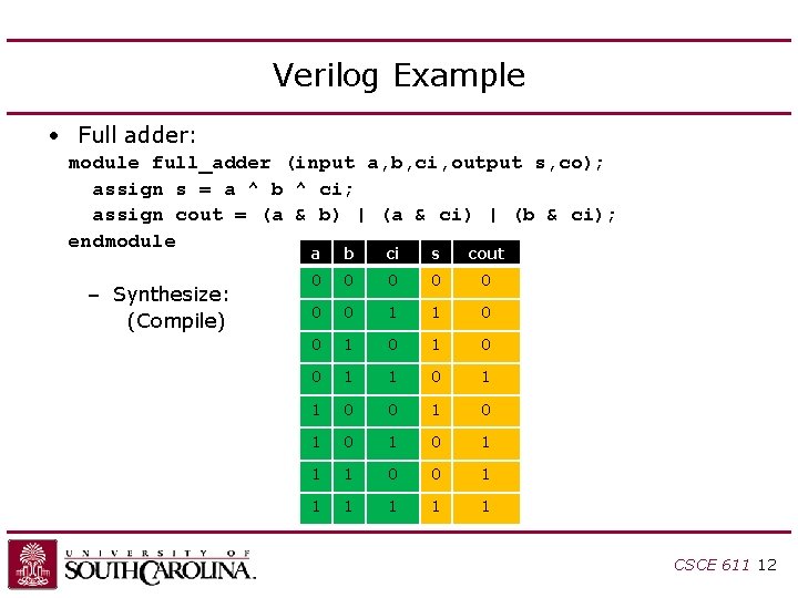
Verilog Example • Full adder: module full_adder (input a, b, ci, output s, co); assign s = a ^ b ^ ci; assign cout = (a & b) | (a & ci) | (b & ci); endmodule – Synthesize: (Compile) a b ci s cout 0 0 0 0 1 1 0 0 1 0 1 1 1 0 0 1 1 1 CSCE 611 12
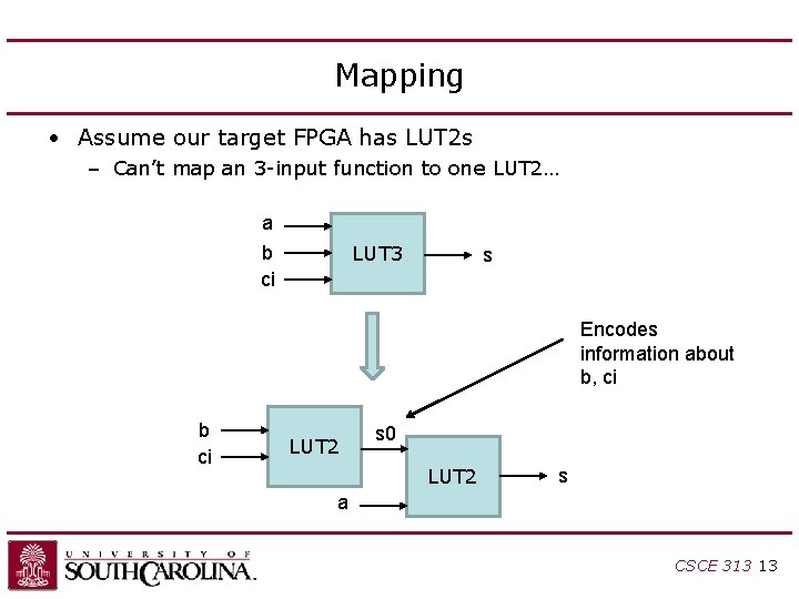
Mapping • Assume our target FPGA has LUT 2 s – Can’t map an 3 -input function to one LUT 2… a b ci LUT 3 s Encodes information about b, ci b ci LUT 2 s 0 LUT 2 s a CSCE 313 13
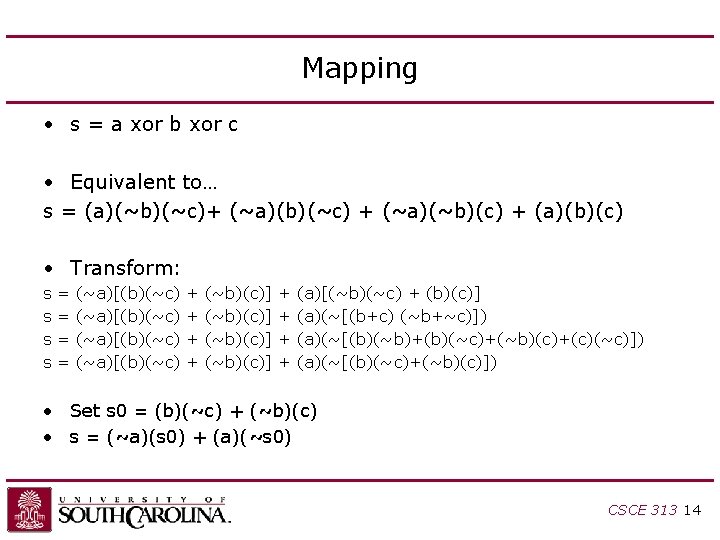
Mapping • s = a xor b xor c • Equivalent to… s = (a)(~b)(~c)+ (~a)(b)(~c) + (~a)(~b)(c) + (a)(b)(c) • Transform: s s = = (~a)[(b)(~c) + + (~b)(c)] + + (a)[(~b)(~c) + (b)(c)] (a)(~[(b+c) (~b+~c)]) (a)(~[(b)(~b)+(b)(~c)+(~b)(c)+(c)(~c)]) (a)(~[(b)(~c)+(~b)(c)]) • Set s 0 = (b)(~c) + (~b)(c) • s = (~a)(s 0) + (a)(~s 0) CSCE 313 14
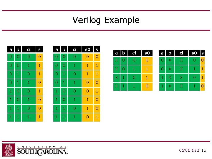
Verilog Example a b ci s 0 s 0 0 0 1 1 0 0 1 1 1 0 1 0 1 1 0 0 1 1 0 0 0 1 1 0 1 0 1 1 0 1 1 1 1 0 1 a b ci s 0 s X 0 0 X 0 1 1 0 X X 1 1 X 1 0 1 1 X X 0 1 X 1 1 0 1 X X 1 0 CSCE 611 15
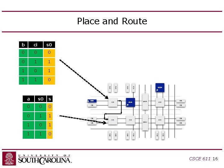
Place and Route b ci s 0 0 0 1 1 1 0 a s 0 0 0 0 1 1 1 0 CSCE 611 16
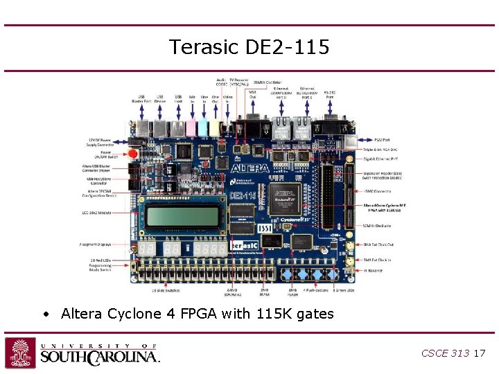
Terasic DE 2 -115 • Altera Cyclone 4 FPGA with 115 K gates CSCE 313 17
System Design • Processors communicate with the outside world using a simple transactional model: – READ: • Processor says READ and provides an address • Operations that depend on this data WAIT until data is returned – WRITE: • Processor says WRITE and provides an address and data • These operations correspond to the LOAD and STORE instructions • In this case, we assume that CPU is the master and devices responding to these operations are slaves CSCE 313 18
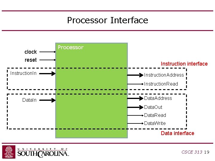
Processor Interface clock reset Instruction. In Processor Instruction interface Instruction. Address Instruction. Read Data. In Data. Address Data. Out Data. Read Data. Write Data interface CSCE 313 19
Programmed I/O • Loads and stores to specially-mapped address ranges can be used to: – Read a word from a status register • Used to poll the state of a peripheral – Write a word to a control register • Used to send an “instruction” to a peripheral CSCE 611 20
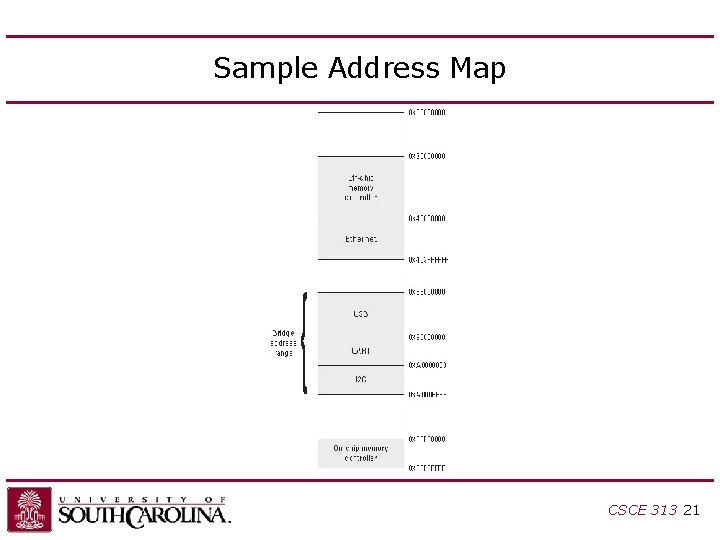
Sample Address Map CSCE 313 21
Altera Tools • Quartus II – Starting point for all designs (create and open projects) – Contains simple editors for HDL design and constraint files – Has a makefile-like design flow manager for synthesis, map, place and route, bitstream generation, and programming • Platform Designer – Allows for drag-and-drop creations of platform designs (processors, busses, peripherals) • Command line tools – Compiler and run code on NIOS 2 processor CSCE 313 22
Platform Designer • Platform Designer allows you to design the portion of your embedded system that is implemented on the FPGA • Using this information, the command-line tools can generate a BSP that corresponds to your system • The BSP includes the interface code for the peripherals that you add in SOPC Builder – As such, it must be regenerated each time you make a change in your system design CSCE 313 23
Setup Your Environment • Do this once: – Open ~/. bashrc – Add a line: source /usr/local/3 rdparty/cad_setup_files/altera. bash – Log out, log back in • Launch Quartus: quartus& CSCE 313 24
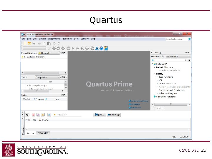
Quartus CSCE 313 25
Creating a New Project • • File | New Quartus II Project… Working directory = /acct/<username>/lights Project name = “lights” Top-level design entity = “lights” “Empty project” Skip the “Add Files” page For device, choose – – – Family: Cyclone IV E Package: FBGA Pin count: 780 Speed grade: 7 Device: EP 4 CE 115 F 29 C 7 • Click Finish • Go to Tools | Platform Designer CSCE 313 26
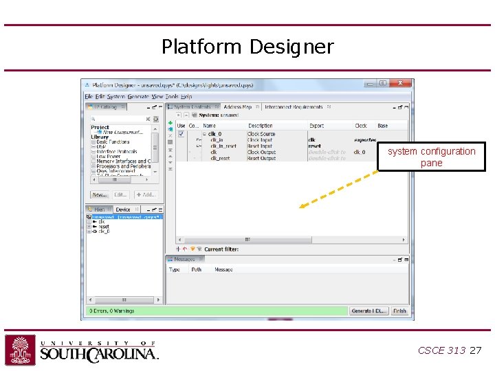
Platform Designer system configuration pane CSCE 313 27
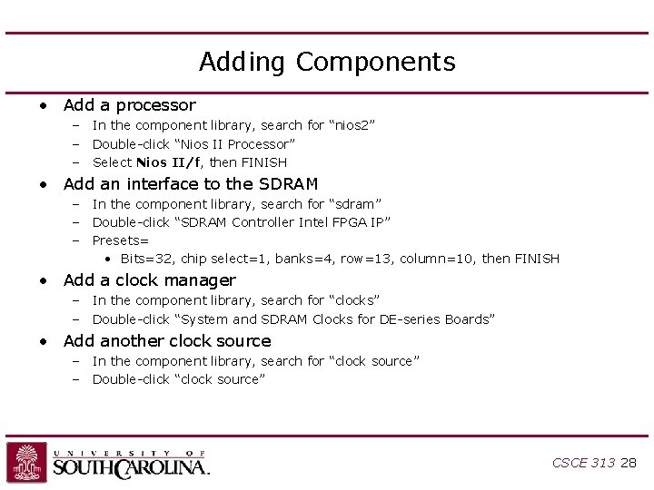
Adding Components • Add a processor – In the component library, search for “nios 2” – Double-click “Nios II Processor” – Select Nios II/f, then FINISH • Add an interface to the SDRAM – In the component library, search for “sdram” – Double-click “SDRAM Controller Intel FPGA IP” – Presets= • Bits=32, chip select=1, banks=4, row=13, column=10, then FINISH • Add a clock manager – In the component library, search for “clocks” – Double-click “System and SDRAM Clocks for DE-series Boards” • Add another clock source – In the component library, search for “clock source” – Double-click “clock source” CSCE 313 28
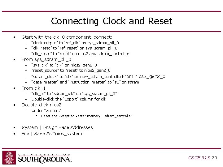
Connecting Clock and Reset • Start with the clk_0 component, connect: – – – • • From sys_sdram_pll_0: – – “sys_clk” to “clk” on nios 2_gen 2_0 “reset_source” to “reset” to nios 2_gen 2_0 – – “sdram_clock” to “clk” on new_sdram_controller From nios 2_gen 2_0 “data_master” and “instruction_master” to “s 1” on sdram From clk_1 – – • “clock output” to “ref_clk” on sys_sdram_pll_0 “clk_reset” to “ref_reset” on sys_sdram_pll_0 “clk_reset” to “reset” on nios 2 and sdram_controller “clk_in” to “sdram_clk” on “sys_sdram_pll_0” Double-click the “Export” column for clk Double-click nios 2 – Under “Vectors” • • • Reset and Exception vector memory: sdram_controller System | Assign Base Addresses File | Save As “nios_system” CSCE 313 29
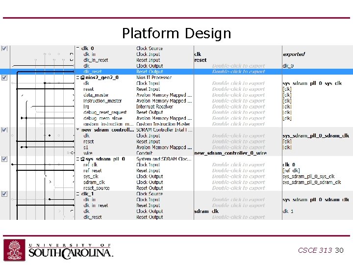
Platform Design CSCE 313 30
Platform Design • Click “Generate HDL” – Accept default settings • Go back to Quartus – Assignments | Import Assignments • “/usr/local/3 rdparty/csce 611/CPU_support_files/DE 2_115_pin_assignments. qsf” – Assignments | Settings • Files | Add | “nios_system. qsys” – File | New | Synopsys Design Constraint File • Contents: create_clock -name CLOCK_50 -period 20 [get_ports CLOCK_50] derive_pll_clocks -create_base_clocks • Save as SDC 1. sdc – File | New | Verilog HDL File • Contents: CSCE 313 31
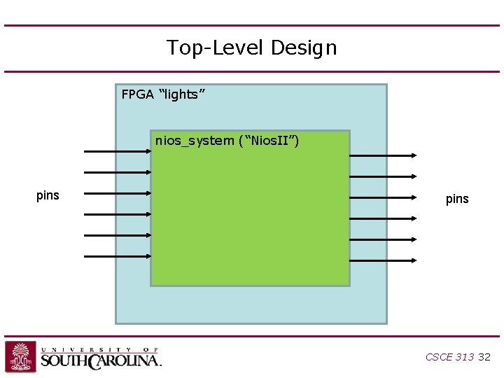
Top-Level Design FPGA “lights” nios_system (“Nios. II”) pins CSCE 313 32
![lights. v module lights (input CLOCK_50, input [3: 0] KEY, output [12: 0] DRAM_ADDR, lights. v module lights (input CLOCK_50, input [3: 0] KEY, output [12: 0] DRAM_ADDR,](http://slidetodoc.com/presentation_image_h/1fd305080bc5f6867eb63bd39878948f/image-33.jpg)
lights. v module lights (input CLOCK_50, input [3: 0] KEY, output [12: 0] DRAM_ADDR, output [1: 0] DRAM_BA, output DRAM_CAS_N, output DRAM_CKE, output DRAM_CS_N, inout [31: 0] DRAM_DQ, output [3: 0] DRAM_DQM, output DRAM_RAS_N, output DRAM_WE_N, output DRAM_CLK); nios_system u 0 (. clk_clk (CLOCK_50), // clk. reset_n (KEY[0]), // reset_n. new_sdram_controller_0_wire_addr (DRAM_ADDR), // new_sdram_controller_0_wire. addr. new_sdram_controller_0_wire_ba (DRAM_BA), //. ba. new_sdram_controller_0_wire_cas_n (DRAM_CAS_N), //. cas_n. new_sdram_controller_0_wire_cke (DRAM_CKE), //. cke. new_sdram_controller_0_wire_cs_n (DRAM_CS_N), //. cs_n. new_sdram_controller_0_wire_dq (DRAM_DQ), //. dq. new_sdram_controller_0_wire_dqm (DRAM_DQM), //. dqm. new_sdram_controller_0_wire_ras_n (DRAM_RAS_N), //. ras_n. new_sdram_controller_0_wire_we_n (DRAM_WE_N), //. we_n. sdram_clk (DRAM_CLK) ); endmodule CSCE 313 33
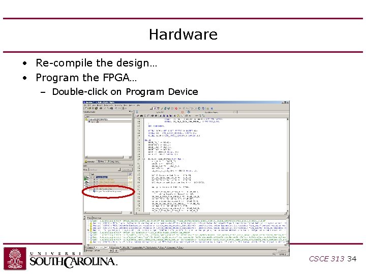
Hardware • Re-compile the design… • Program the FPGA… – Double-click on Program Device CSCE 313 34
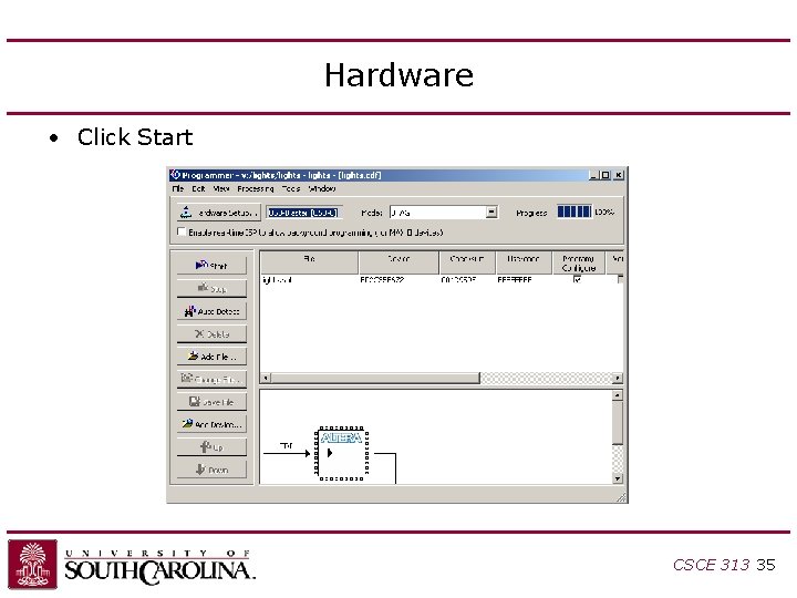
Hardware • Click Start CSCE 313 35
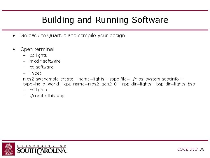
Building and Running Software • Go back to Quartus and compile your design • Open terminal – cd lights – mkdir software – cd software – Type: nios 2 -swexample-create --name=lights --sopc-file=. . /nios_system. sopcinfo -type=hello_world --cpu-name=nios 2_gen 2_0 --app-dir=lights --bsp-dir=lights_bsp – cd lights –. /create-this-app CSCE 313 36
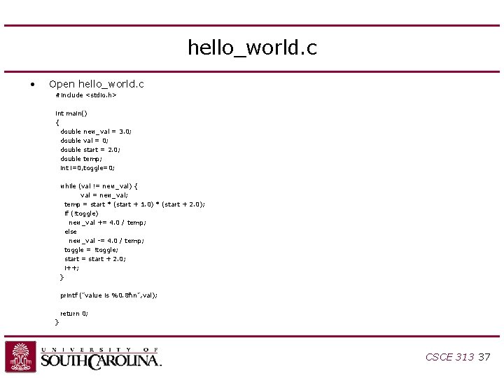
hello_world. c • Open hello_world. c #include <stdio. h> int main() { double new_val = 3. 0; double val = 0; double start = 2. 0; double temp; int i=0, toggle=0; while (val != new_val) { val = new_val; temp = start * (start + 1. 0) * (start + 2. 0); if (!toggle) new_val += 4. 0 / temp; else new_val -= 4. 0 / temp; toggle = !toggle; start = start + 2. 0; i++; } printf ("value is %0. 8 fn", val); return 0; } CSCE 313 37
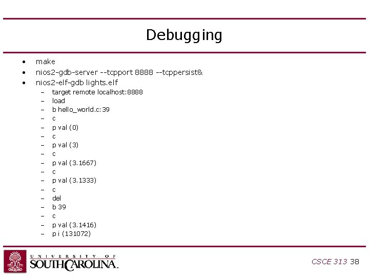
Debugging • • • make nios 2 -gdb-server --tcpport 8888 --tcppersist& nios 2 -elf-gdb lights. elf – – – – – target remote localhost: 8888 load b hello_world. c: 39 c p val (0) c p val (3. 1667) c p val (3. 1333) c del b 39 c p val (3. 1416) p i (131072) CSCE 313 38
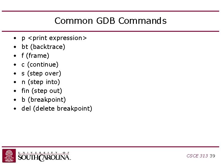
Common GDB Commands • • • p <print expression> bt (backtrace) f (frame) c (continue) s (step over) n (step into) fin (step out) b (breakpoint) del (delete breakpoint) CSCE 313 39
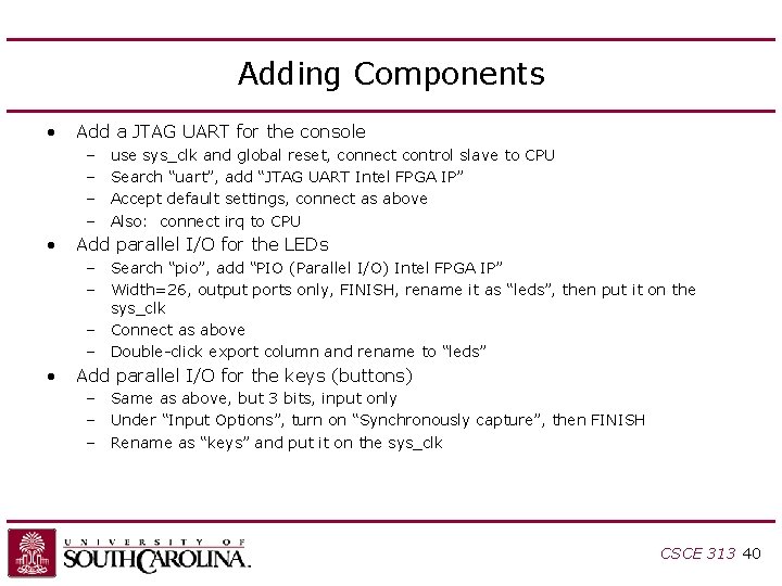
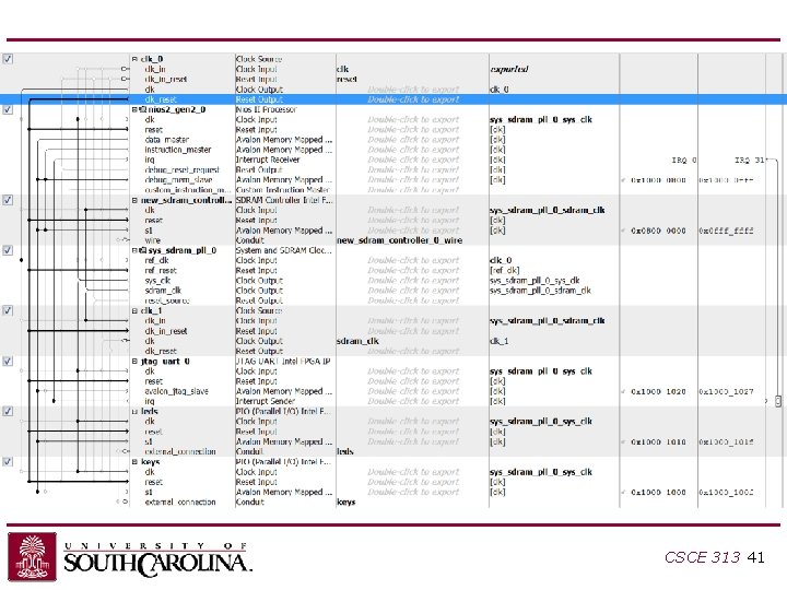
Adding Components • Add a JTAG UART for the console – – • use sys_clk and global reset, connect control slave to CPU Search “uart”, add “JTAG UART Intel FPGA IP” Accept default settings, connect as above Also: connect irq to CPU Add parallel I/O for the LEDs – Search “pio”, add “PIO (Parallel I/O) Intel FPGA IP” – Width=26, output ports only, FINISH, rename it as “leds”, then put it on the sys_clk – Connect as above – Double-click export column and rename to “leds” • Add parallel I/O for the keys (buttons) – Same as above, but 3 bits, input only – Under “Input Options”, turn on “Synchronously capture”, then FINISH – Rename as “keys” and put it on the sys_clk CSCE 313 40
Adding Components CSCE 313 41
![lights. v module lights (input CLOCK_50, input [3: 0] KEY, output [12: 0] DRAM_ADDR, lights. v module lights (input CLOCK_50, input [3: 0] KEY, output [12: 0] DRAM_ADDR,](http://slidetodoc.com/presentation_image_h/1fd305080bc5f6867eb63bd39878948f/image-42.jpg)
lights. v module lights (input CLOCK_50, input [3: 0] KEY, output [12: 0] DRAM_ADDR, output [1: 0] DRAM_BA, output DRAM_CAS_N, output DRAM_CKE, output DRAM_CS_N, inout [31: 0] DRAM_DQ, output [3: 0] DRAM_DQM, output DRAM_RAS_N, output DRAM_WE_N, output DRAM_CLK, output [17: 0] LEDR, output [7: 0] LEDG ); nios_system u 0 (. clk_clk (CLOCK_50), // clk. reset_n (KEY[0]), // reset_n. new_sdram_controller_0_wire_addr (DRAM_ADDR), // new_sdram_controller_0_wire. addr. new_sdram_controller_0_wire_ba (DRAM_BA), //. ba. new_sdram_controller_0_wire_cas_n (DRAM_CAS_N), //. cas_n. new_sdram_controller_0_wire_cke (DRAM_CKE), //. cke. new_sdram_controller_0_wire_cs_n (DRAM_CS_N), //. cs_n. new_sdram_controller_0_wire_dq (DRAM_DQ), //. dq. new_sdram_controller_0_wire_dqm (DRAM_DQM), //. dqm. new_sdram_controller_0_wire_ras_n (DRAM_RAS_N), //. ras_n. new_sdram_controller_0_wire_we_n (DRAM_WE_N), //. we_n. sdram_clk (DRAM_CLK), . keys_export (KEY[3: 1]), // keys. export. leds_export ({LEDR, LEDG}), // leds. export ); endmodule CSCE 313 42
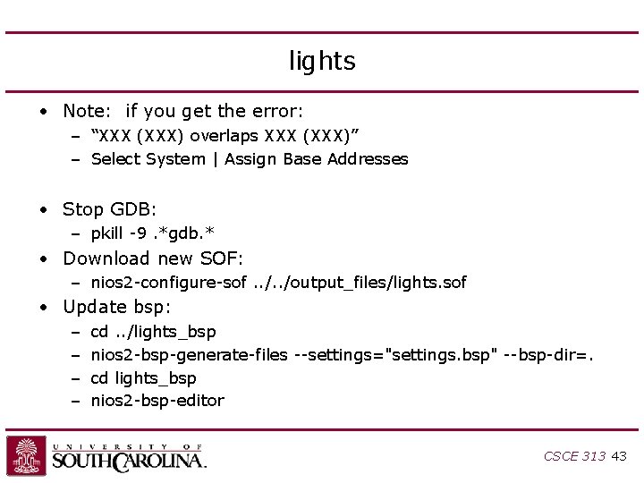
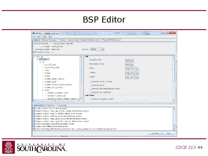
lights • Note: if you get the error: – “XXX (XXX) overlaps XXX (XXX)” – Select System | Assign Base Addresses • Stop GDB: – pkill -9. *gdb. * • Download new SOF: – nios 2 -configure-sof. . /output_files/lights. sof • Update bsp: – – cd. . /lights_bsp nios 2 -bsp-generate-files --settings="settings. bsp" --bsp-dir=. cd lights_bsp nios 2 -bsp-editor CSCE 313 43
BSP Editor CSCE 313 44
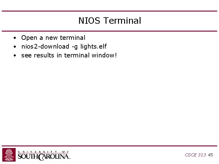
NIOS Terminal • Open a new terminal • nios 2 -download -g lights. elf • see results in terminal window! CSCE 313 45
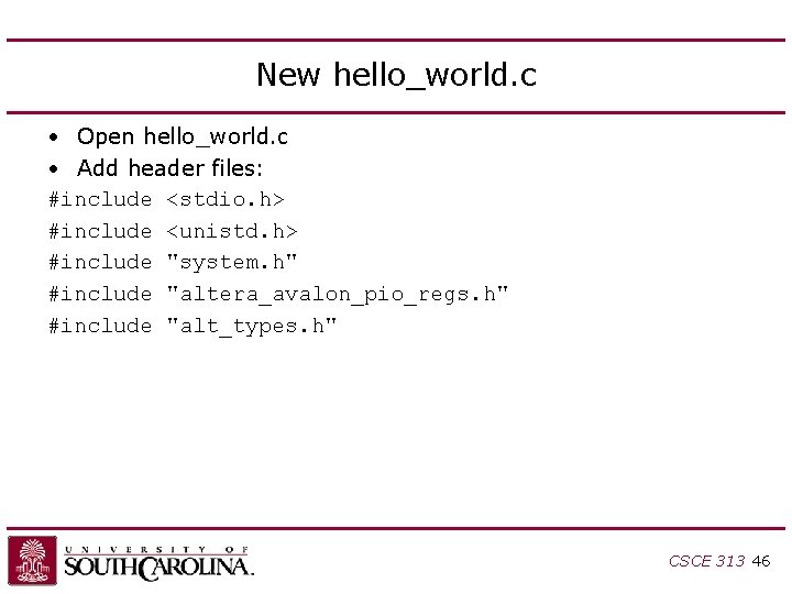
New hello_world. c • Open hello_world. c • Add header files: #include <stdio. h> #include <unistd. h> #include "system. h" #include "altera_avalon_pio_regs. h" #include "alt_types. h" CSCE 313 46
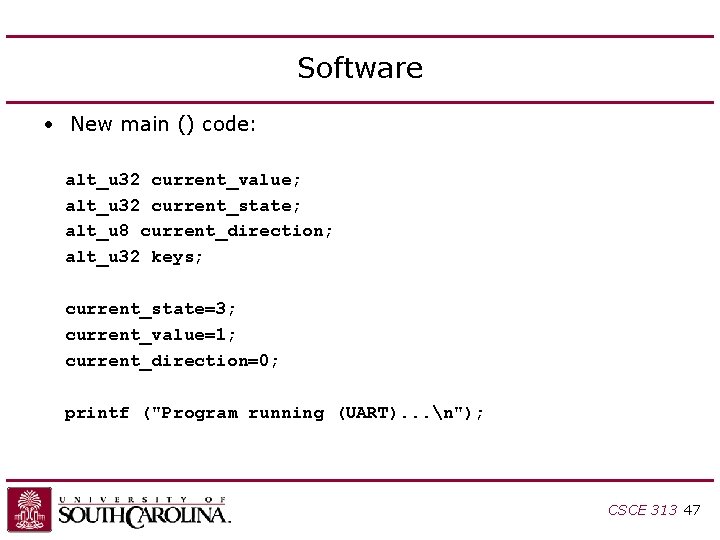
Software • New main () code: alt_u 32 current_value; alt_u 32 current_state; alt_u 8 current_direction; alt_u 32 keys; current_state=3; current_value=1; current_direction=0; printf ("Program running (UART). . . n"); CSCE 313 47
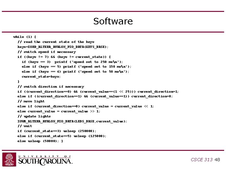
Software while (1) { // read the current state of the keys=IORD_ALTERA_AVALON_PIO_DATA(KEYS_BASE); // switch speed if necessary if ((keys != 7) && (keys != current_state)) { if (keys == 3) printf ("speed set to 250 msn"); else if (keys == 5) printf ("speed set to 150 msn"); else if (keys == 6) printf ("speed set to 50 msn"); current_state=keys; } // switch direction if necessary if ((current_direction==0) && (current_value==(1 << 25))) current_direction=1; else if ((current_direction==1) && (current_value==1)) current_direction=0; // move light else if (current_direction==0) current_value = current_value << 1; else current_value = current_value >> 1; // update lights IOWR_ALTERA_AVALON_PIO_DATA(LEDS_BASE, current_value); // wait if (current_state==3) usleep (250000); else if (current_state==5) usleep (125000); else usleep (50000); } CSCE 313 48
Quartus • Back to Quartus… • Now we need to write a top-level Verilog HDL file for lights • File | New | Verilog HDL File CSCE 313 49
- Slides: 49