CSCE 230 Fall 2013 Appendix A Logic Circuits






- Slides: 53

CSCE 230, Fall 2013 Appendix A: Logic Circuits, part 1 Logic Circuits Mehmet Can Vuran, Instructor University of Nebraska-Lincoln Acknowledgement: Overheads adapted from those provided by the authors of the textbook

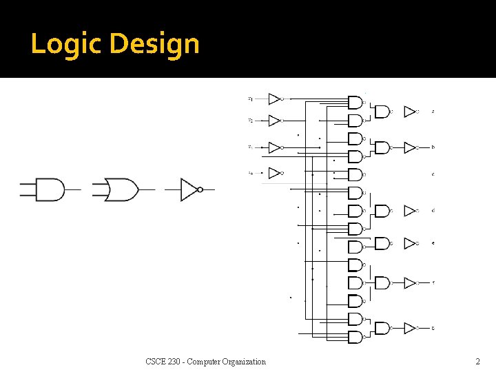
Logic Design CSCE 230 - Computer Organization 2

Logic Design CSCE 230 - Computer Organization 3

Logic Implementation Choices � Programmable Software ▪ Typically, use single-board microcontrollers to implement the logic by a program Programmable logic devices (PLDs) and field programmable gate arrays (FPGAs) ▪ Devices in which the logic elements and the interconnect (wiring) can be modified by programming. ▪ Ideal for rapid prototyping and low-volume applications. ROMs �Custom Designs How Intel designs microprocessors Cost-effective only for high-volume parts CSCE 230 - Computer Organization 4

Logic circuits � Operate on binary variables that assume one of two distinct values, usually called 0 and 1 � Implement functions of logic variables � Circuits have inputs and outputs � Circuits are implemented using electronic logic gates

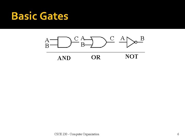
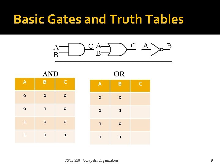
Basic Gates CA B AND C OR CSCE 230 - Computer Organization A B NOT 6

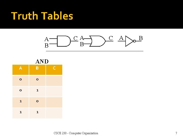
Truth Tables CA B C A B AND A B 0 0 0 1 1 C CSCE 230 - Computer Organization 7

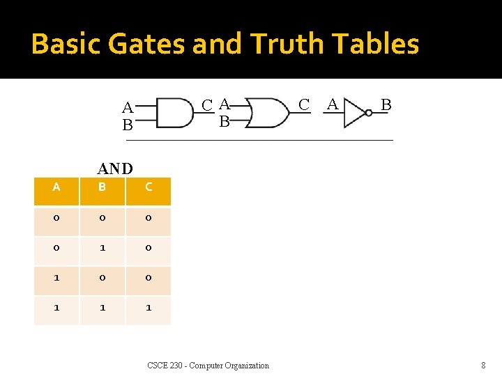
Basic Gates and Truth Tables CA B C A B AND A B C 0 0 1 1 1 CSCE 230 - Computer Organization 8

Basic Gates and Truth Tables CA B AND A C B OR A B C A B 0 0 0 1 0 1 1 1 CSCE 230 - Computer Organization C 9

Basic Gates and Truth Tables CA B AND A C B OR A B C 0 0 0 0 1 1 1 0 0 1 1 1 1 CSCE 230 - Computer Organization 10

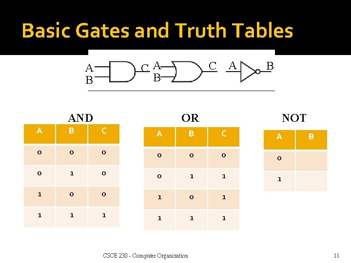
Basic Gates and Truth Tables CA B AND A C B OR NOT A B C A 0 0 0 0 1 1 0 0 1 1 1 1 CSCE 230 - Computer Organization B 11

Basic Gates and Truth Tables CA B AND A C B OR NOT A B C A B 0 0 0 0 1 1 1 0 0 1 1 1 1 CSCE 230 - Computer Organization 12

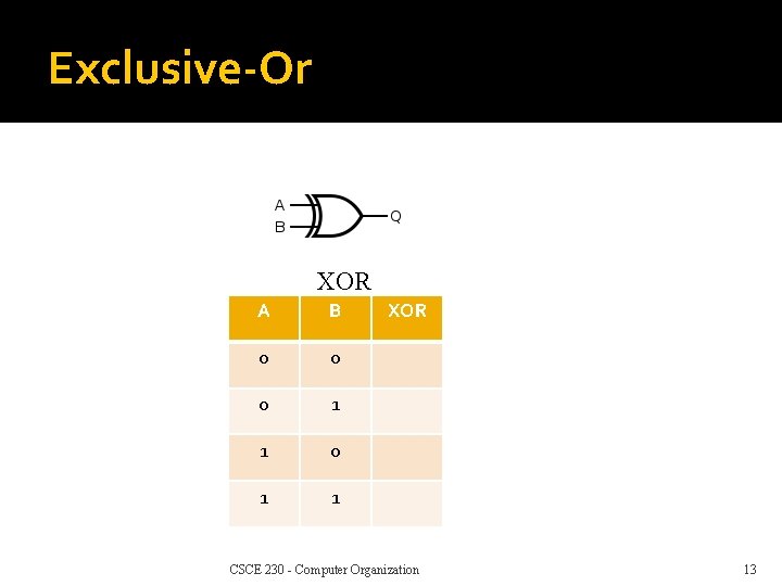
Exclusive-Or XOR A B 0 0 0 1 1 XOR CSCE 230 - Computer Organization 13

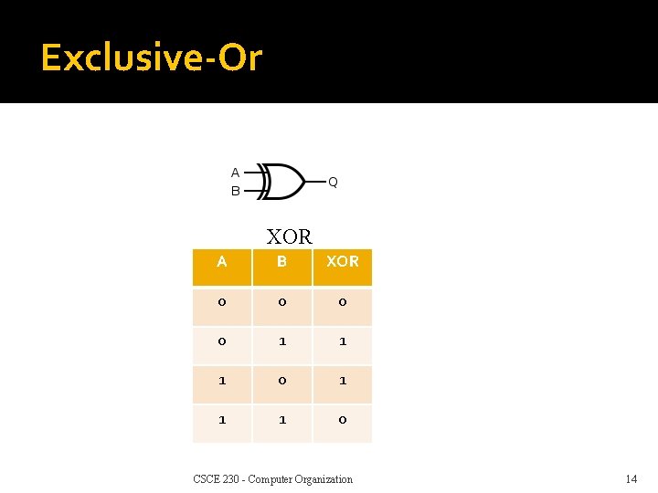
Exclusive-Or XOR A B XOR 0 0 1 1 1 0 CSCE 230 - Computer Organization 14

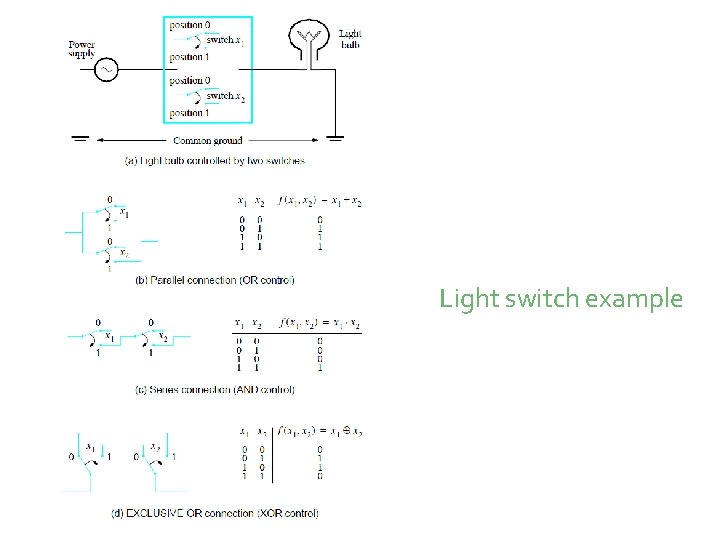
Light switch example

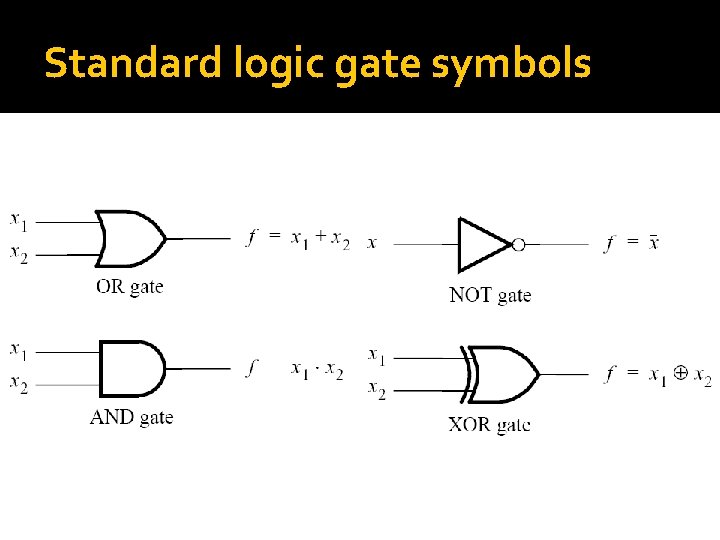
Standard logic gate symbols

Why? How?

Logic circuits � Operate on binary variables that assume one of two distinct values, usually called 0 and 1 � Why? � Let’s back up…

Let’s Back up…

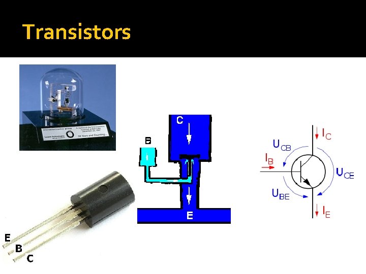
Transistors

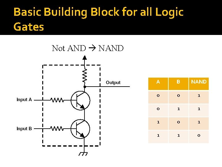
Basic Building Block for all Logic Gates Not AND NAND A B NAND 0 0 1 1 1 0

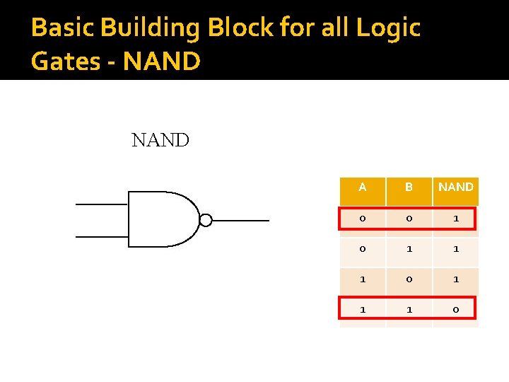
Basic Building Block for all Logic Gates - NAND A B NAND 0 0 1 1 1 0

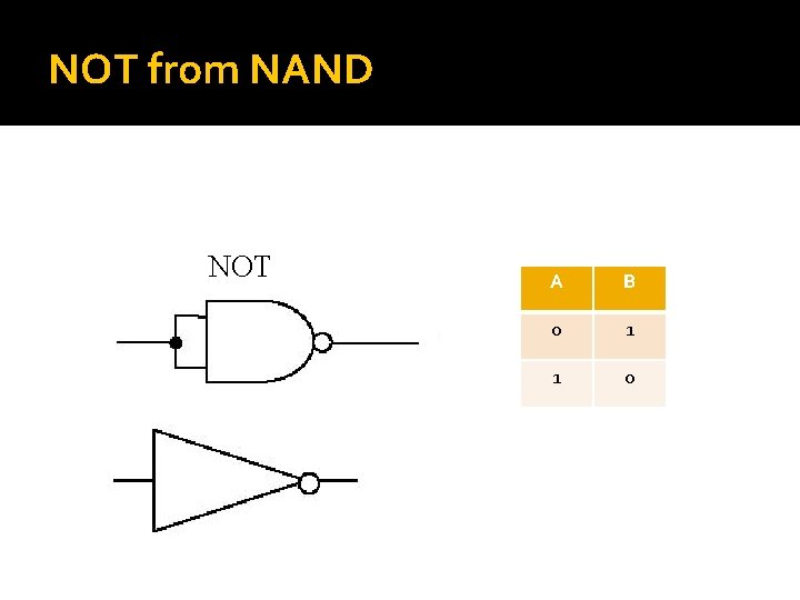
NOT from NAND NOT A B 0 1 1 0

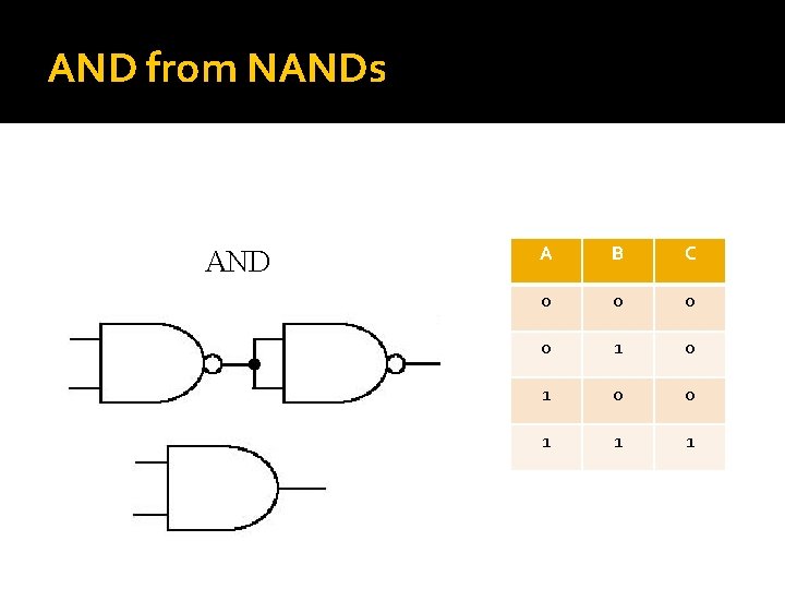
AND from NANDs AND A B C 0 0 1 1 1

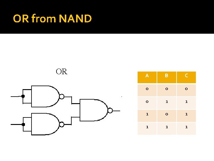
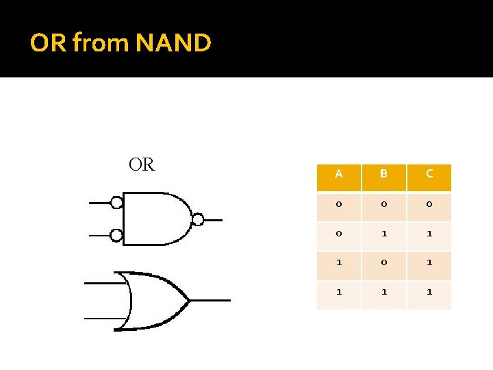
OR from NAND OR A B C 0 0 1 1 1 0 1 1

OR from NAND OR A B C 0 0 1 1 1 0 1 1

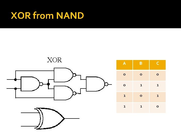
XOR from NAND XOR A B C 0 0 1 1 1 0

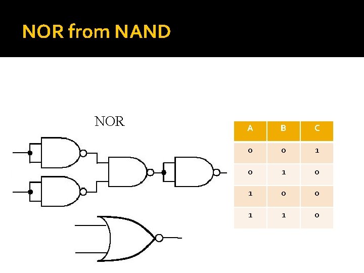
NOR from NAND NOR A B C 0 0 1 0 1 0 0 1 1 0

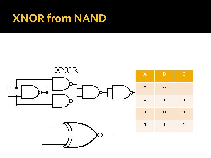
XNOR from NAND XNOR A B C 0 0 1 0 1 0 0 1 1 1

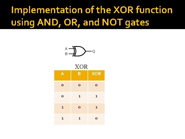
Implementation of the XOR function using AND, OR, and NOT gates XOR A B XOR 0 0 1 1 1 0

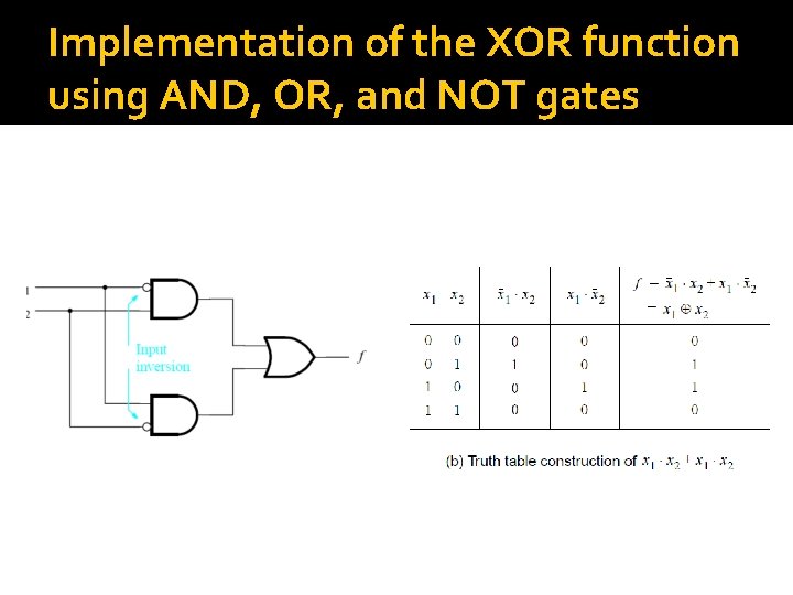
Implementation of the XOR function using AND, OR, and NOT gates

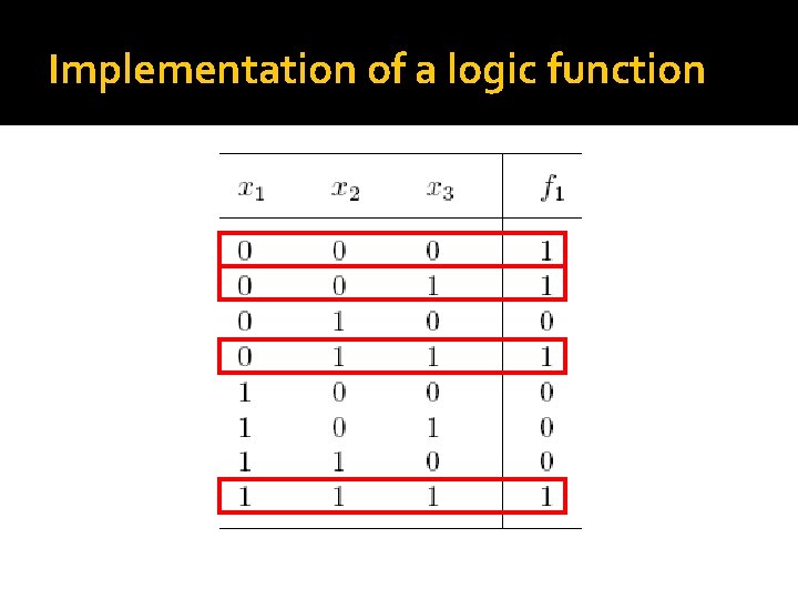
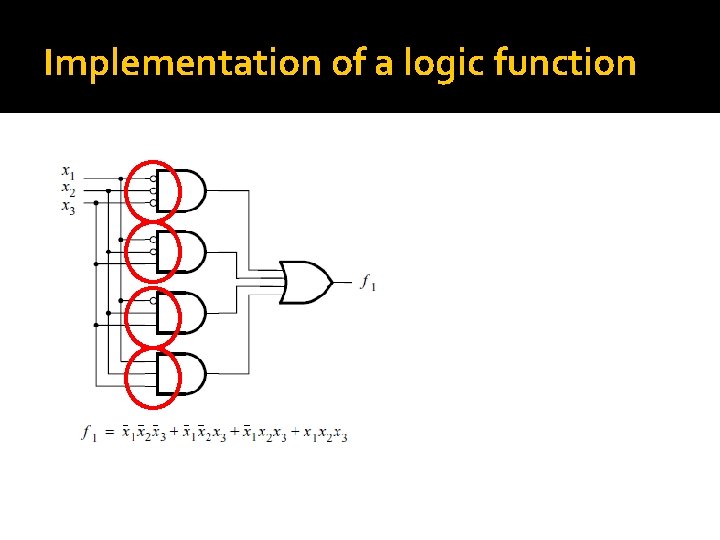
Synthesis of logic functions �Synthesis is the process of designing and implementing a logic circuit defined by its functional specification. �The expression for f in the previous circuit is said to be in a sum-of-products form OR and AND operations are sometimes called the sum and product functions.

Implementation of a logic function

Implementation of a logic function

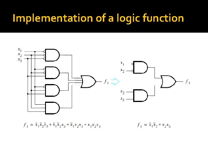
Implementation of a logic function

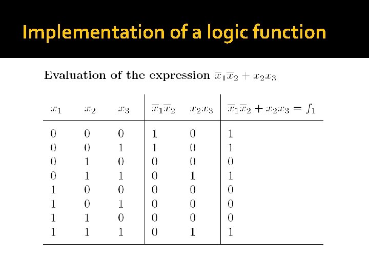
Implementation of a logic function

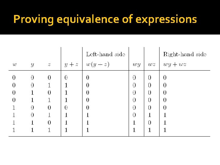
Proving equivalence of expressions

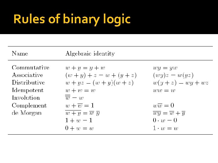
Rules of binary logic

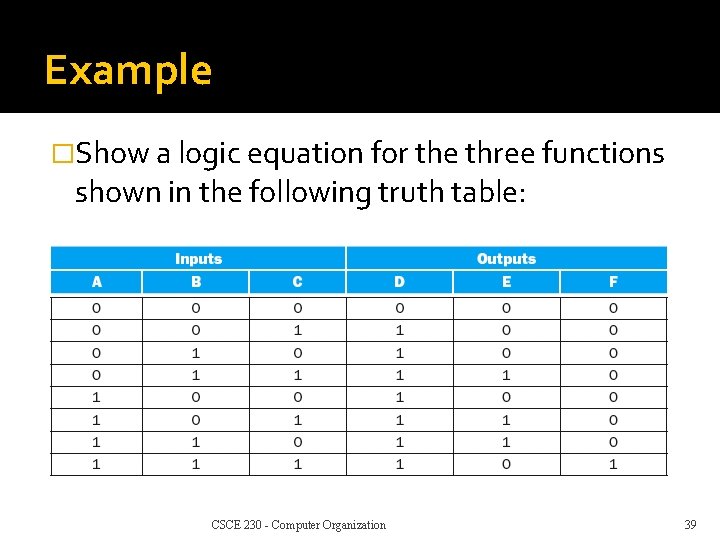
Example �Show a logic equation for the three functions shown in the following truth table: CSCE 230 - Computer Organization 39

Minimization of logic expressions �As illustrated in the previous example, a logic function can be implemented with circuits of different complexities. �It is useful to minimize a logic expression to reduce the cost of the synthesized circuit.

Karnaugh Maps 41

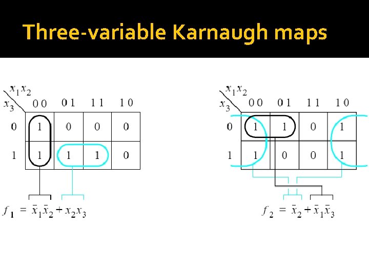
Three-variable Karnaugh maps

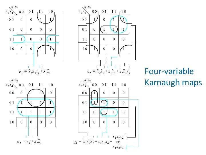
Four-variable Karnaugh maps

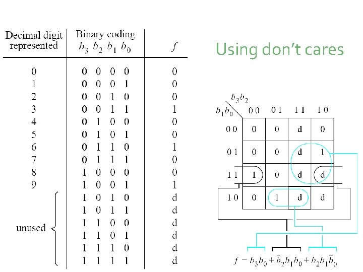
Using don’t cares

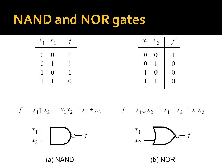
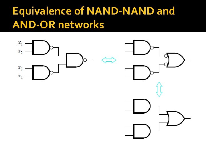
NAND and NOR gates

Equivalence of NAND-NAND and AND-OR networks

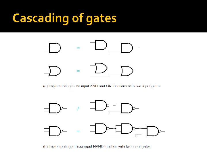
Cascading of gates

Section A. 5 Practical Implementation of Logic Gates Read the Chapter in detail and study the following slides, we will skip most of them in class 48

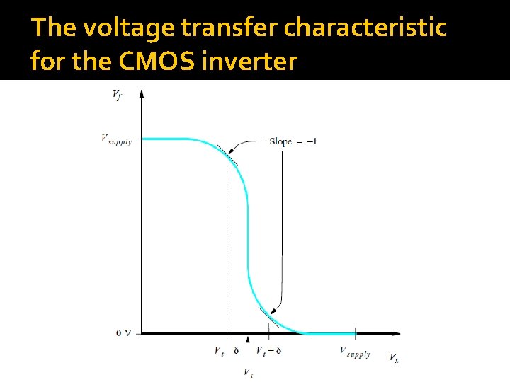
The voltage transfer characteristic for the CMOS inverter

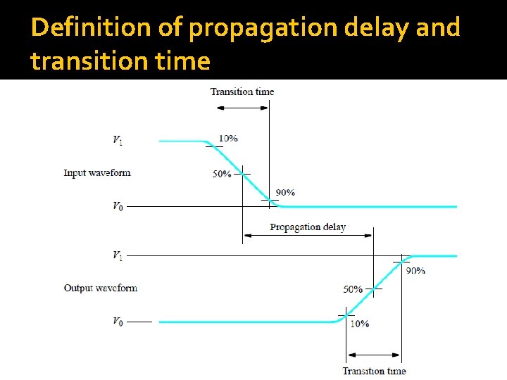
Definition of propagation delay and transition time

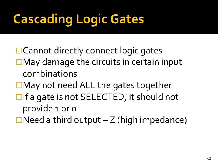
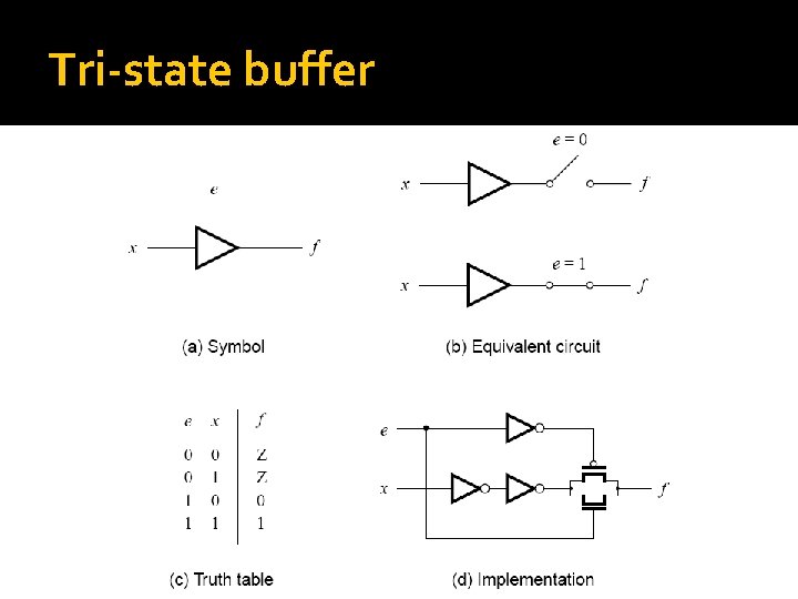
Cascading Logic Gates �Cannot directly connect logic gates �May damage the circuits in certain input combinations �May not need ALL the gates together �If a gate is not SELECTED, it should not provide 1 or 0 �Need a third output – Z (high impedance) 62

Tri-state buffer

Upcoming… �HW 3 – Chapter 3 Assign Friday, Sept. 27 th Due Wednesday, Oct. 9 th �Test 1 – Chapters 1 -2 Monday, Oct. 7 th (50 min) �Quiz 3 – Chapter 3 Friday, Oct. 11 th (15 min) 64