CSCE 211 Digital Design Lecture 14 State Machines
- Slides: 53

CSCE 211 Digital Design Lecture 14 State Machines II Topics n State Machine Design n Resolution with Text l Design with D flip-flops l Design with JK Readings: Chapter 7 November 11, 2015

Overview Last Time n State machine construction l HW $. 50 coke machine with no change New § State machine construction again (text notation) Next Time: n – 2– Test 2 : Nov 16 th next Monday CSCE 211 H Fall 2014

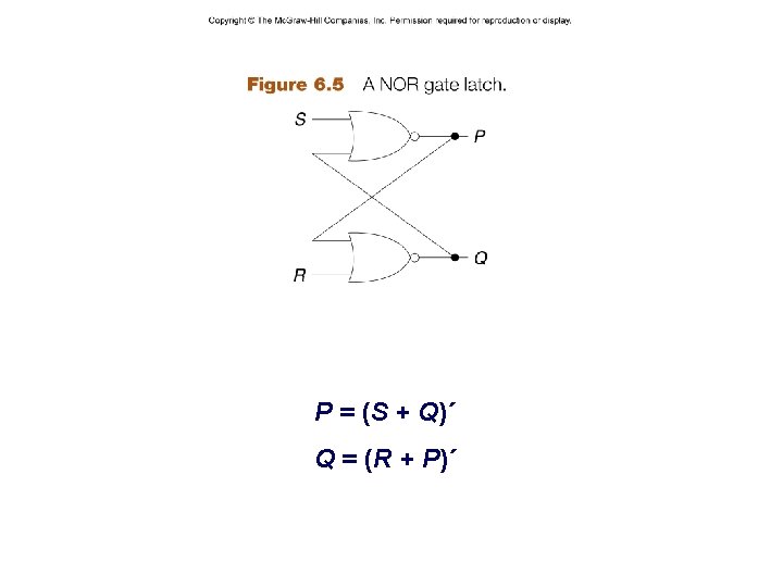
P = (S + Q)´ Q = (R + P)´ – 3– CSCE 211 H Fall 2014

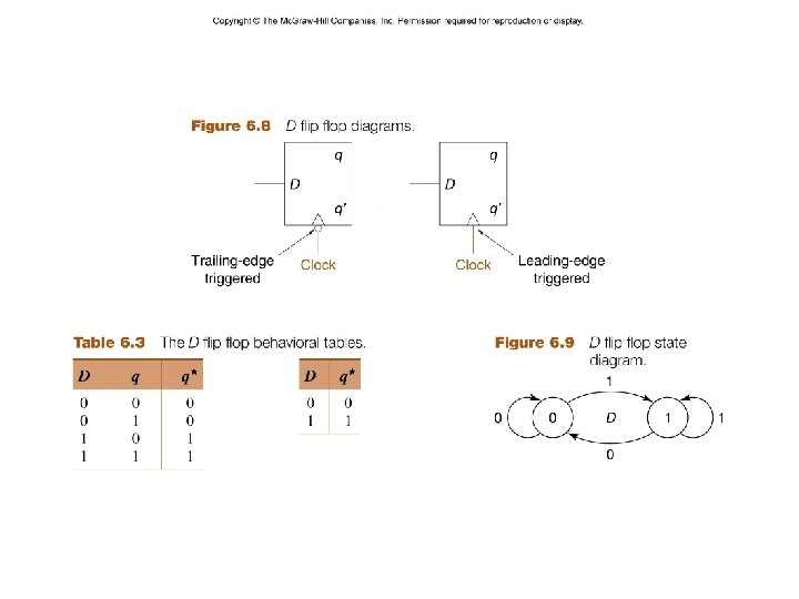
– 4– CSCE 211 H Fall 2014

– 5– CSCE 211 H Fall 2014

– 6– CSCE 211 H Fall 2014

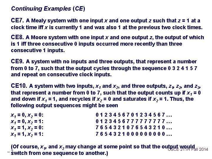
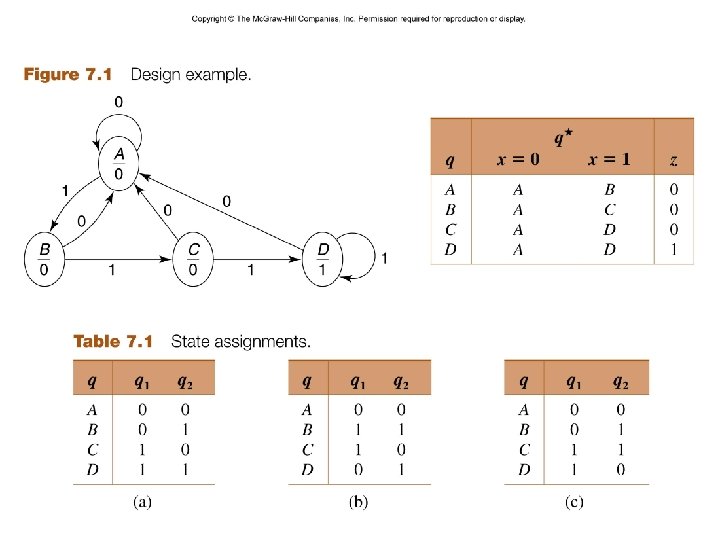
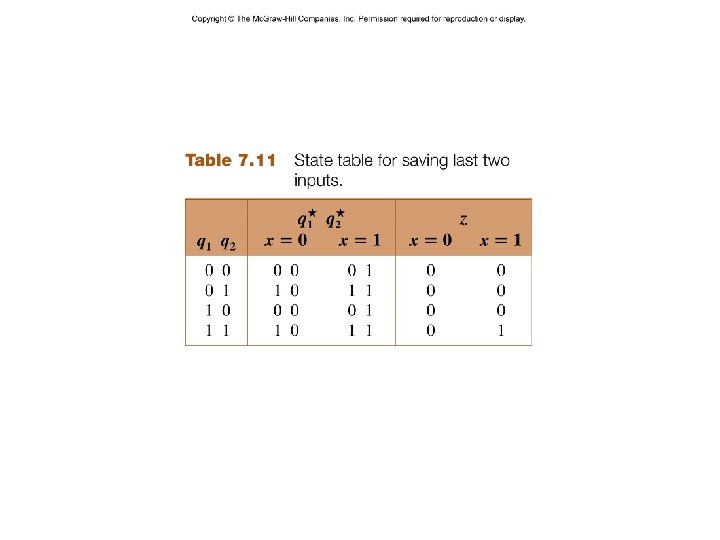
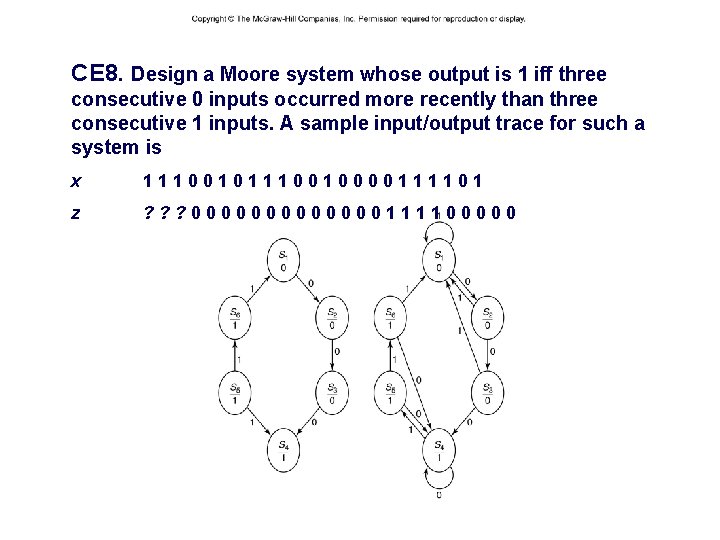
Continuing Examples (CE) CE 7. A Mealy system with one input x and one output z such that z = 1 at a clock time iff x is currently 1 and was also 1 at the previous two clock times. CE 8. A Moore system with one input x and one output z, the output of which is 1 iff three consecutive 0 inputs occurred more recently than three consecutive 1 inputs. CE 9. A system with no inputs and three outputs, that represent a number from 0 to 7, such that the output cycles through the sequence 0 3 2 4 1 5 7 and repeat on consecutive clock inputs. CE 10. A system with two inputs, x 1 and x 2, and three outputs, z 1, z 2, and z 3, that represent a number from 0 to 7, such that the output counts up if x 1 = 0 and down if x 1 = 1, and recycles if x 2 = 0 and saturates if x 2 = 1. Thus, the following output sequences might be seen x 1 = 0, x 2 = 0: x 1 = 0, x 2 = 1: x 1 = 1, x 2 = 0: x 1 = 1, x 2 = 1: 01234567… 012345677777… 76543210… 765432100000… (Of course, x 1, and x 2 may change at some point so that the output would CSCE 211 H Fall 2014 from one sequence to another. ) – 7 – switch

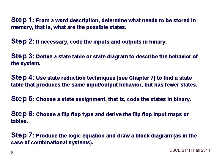
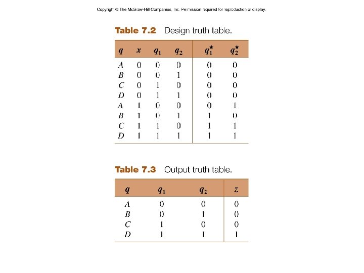
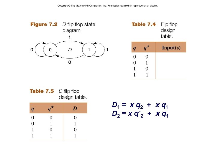
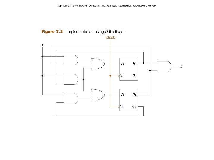
Step 1: From a word description, determine what needs to be stored in memory, that is, what are the possible states. Step 2: If necessary, code the inputs and outputs in binary. Step 3: Derive a state table or state diagram to describe the behavior of the system. Step 4: Use state reduction techniques (see Chapter 7) to find a state table that produces the same input/output behavior, but has fewer states. Step 5: Choose a state assignment, that is, code the states in binary. Step 6: Choose a flip flop type and derive the flip flop input maps or tables. Step 7: Produce the logic equation and draw a block diagram (as in the case of combinational systems). – 8– CSCE 211 H Fall 2014

– 9– CSCE 211 H Fall 2014

– 10 – CSCE 211 H Fall 2014

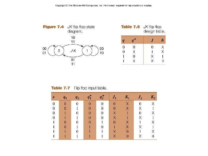
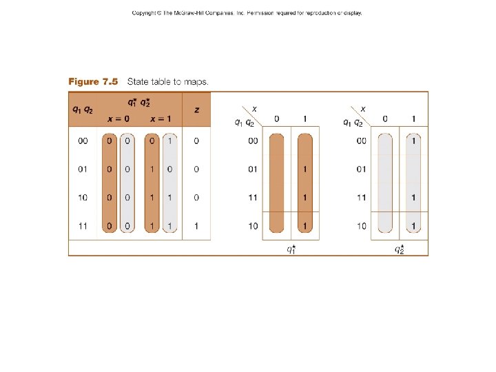
D 1 = x q 2 + x q 1 D 2 = x q´ 2 + x q 1 – 11 – CSCE 211 H Fall 2014

– 12 – CSCE 211 H Fall 2014

– 13 – CSCE 211 H Fall 2014

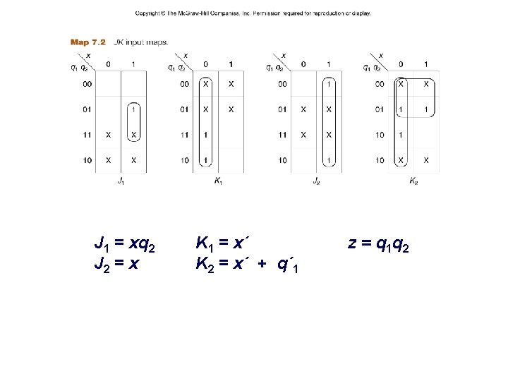
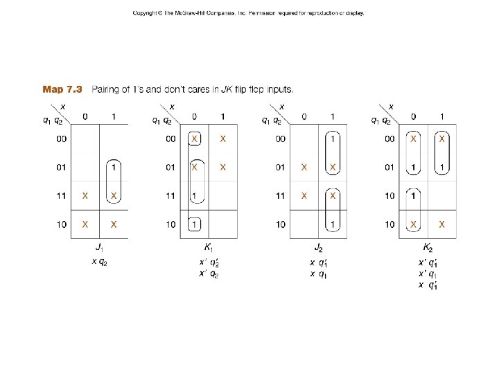
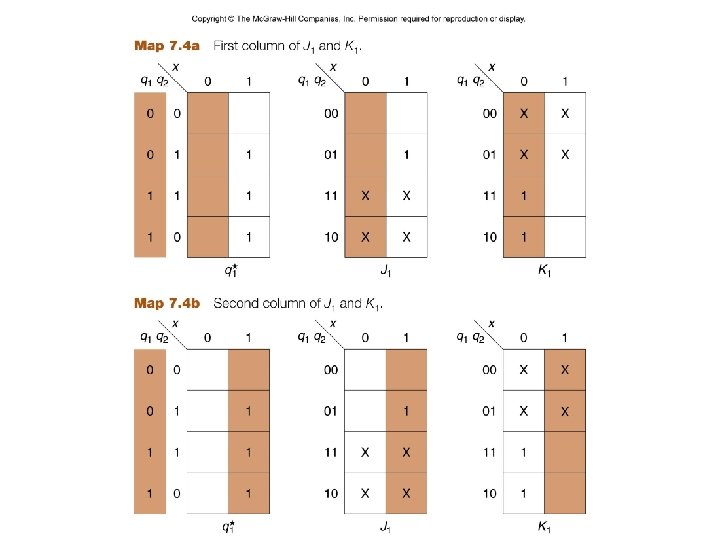
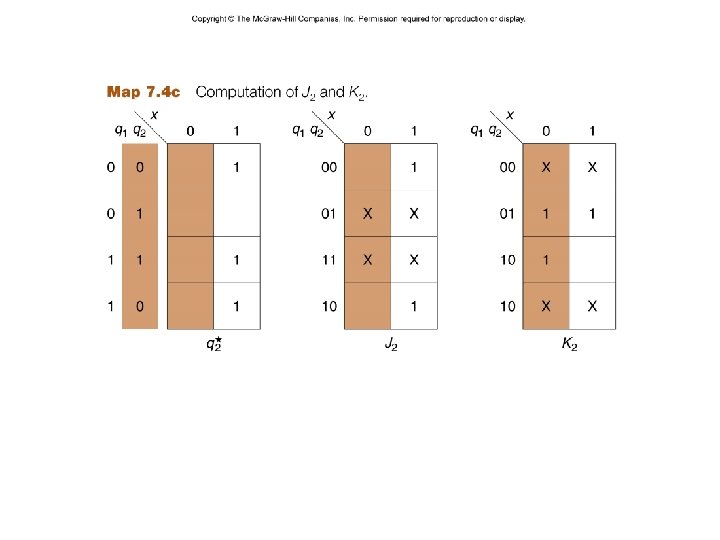
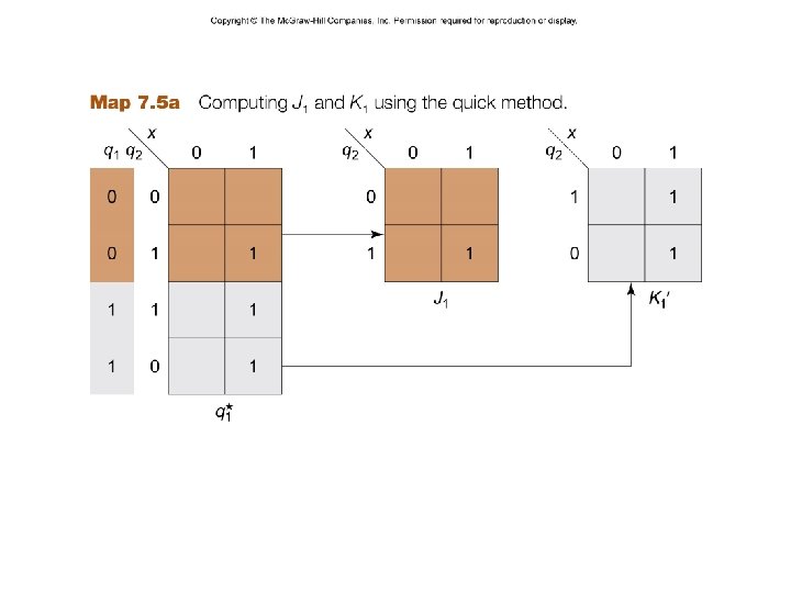
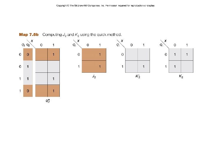
J 1 = xq 2 J 2 = x – 14 – K 1 = x´ K 2 = x´ + q´ 1 z = q 1 q 2 CSCE 211 H Fall 2014

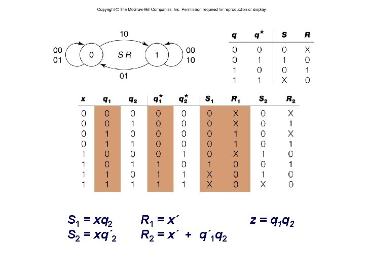
S 1 = xq 2 S 2 = xq´ 2 – 15 – R 1 = x´ R 2 = x´ + q´ 1 q 2 z = q 1 q 2 CSCE 211 H Fall 2014

– 16 – CSCE 211 H Fall 2014

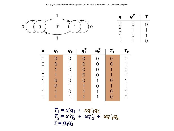
– 17 – T 1 = x´q 1 + xq´ 1 q 2 T 2 = x´q 2 + xq´ 1 q 2 z = q 1 q 2 CSCE 211 H Fall 2014

– 18 – CSCE 211 H Fall 2014

– 19 – CSCE 211 H Fall 2014

– 20 – CSCE 211 H Fall 2014

– 21 – CSCE 211 H Fall 2014

– 22 – CSCE 211 H Fall 2014

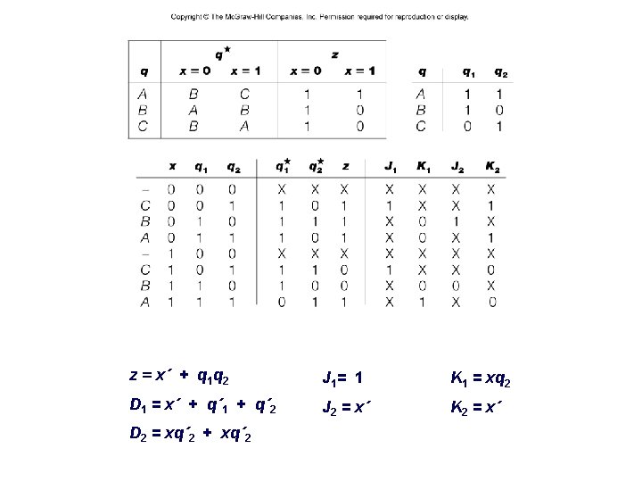
z = x´ + q 1 q 2 J 1 = 1 K 1 = xq 2 D 1 = x´ + q´ 1 + q´ 2 J 2 = x´ K 2 = x´ D 2 = xq´ 2 + xq´ 2 – 23 – CSCE 211 H Fall 2014

– 24 – CSCE 211 H Fall 2014

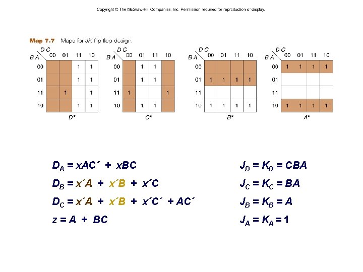
– 25 – DA = x. AC´ + x. BC JD = KD = CBA DB = x´A + x´B + x´C JC = KC = BA DC = x´A + x´B + x´C´ + AC´ JB = KB = A z = A + BC JA = KA = 1 CSCE 211 H Fall 2014

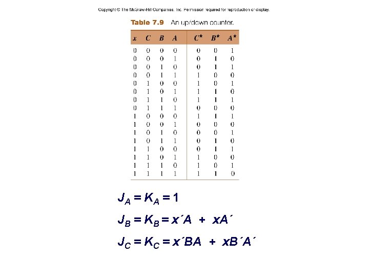
JA = KA = 1 JB = KB = x´A + x. A´ JC = KC = x´BA + x. B´A´ – 26 – CSCE 211 H Fall 2014

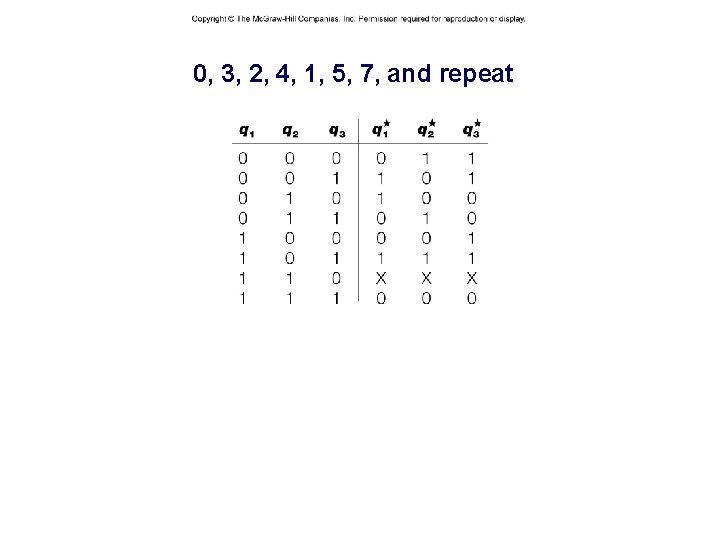
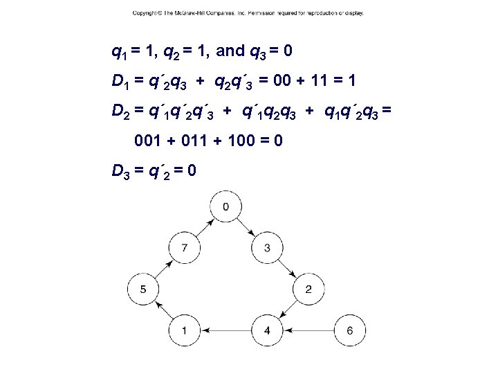
0, 3, 2, 4, 1, 5, 7, and repeat – 27 – CSCE 211 H Fall 2014

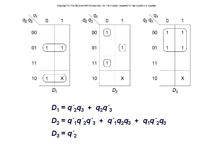
D 1 = q´ 2 q 3 + q 2 q´ 3 D 2 = q´ 1 q´ 2 q´ 3 + q´ 1 q 2 q 3 + q 1 q´ 2 q 3 D 3 = q´ 2 – 28 – CSCE 211 H Fall 2014

q 1 = 1, q 2 = 1, and q 3 = 0 D 1 = q´ 2 q 3 + q 2 q´ 3 = 00 + 11 = 1 D 2 = q´ 1 q´ 2 q´ 3 + q´ 1 q 2 q 3 + q 1 q´ 2 q 3 = 001 + 011 + 100 = 0 D 3 = q´ 2 = 0 – 29 – CSCE 211 H Fall 2014

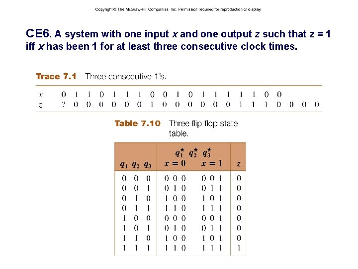
CE 6. A system with one input x and one output z such that z = 1 iff x has been 1 for at least three consecutive clock times. – 30 – CSCE 211 H Fall 2014

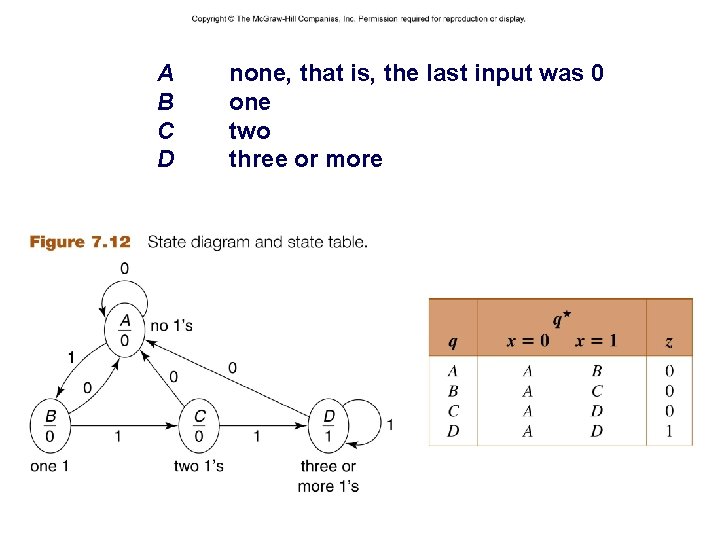
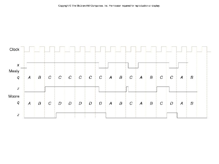
A B C D – 31 – none, that is, the last input was 0 one two three or more CSCE 211 H Fall 2014

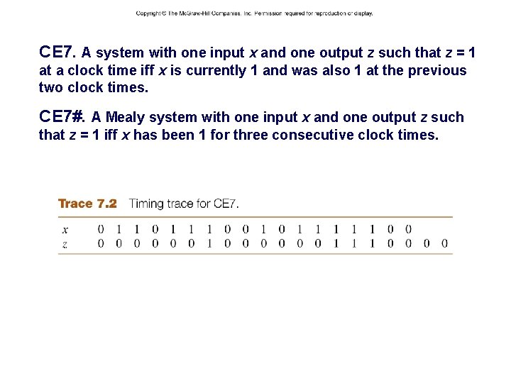
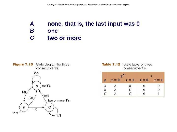
CE 7. A system with one input x and one output z such that z = 1 at a clock time iff x is currently 1 and was also 1 at the previous two clock times. CE 7#. A Mealy system with one input x and one output z such that z = 1 iff x has been 1 for three consecutive clock times. – 32 – CSCE 211 H Fall 2014

– 33 – CSCE 211 H Fall 2014

A B C – 34 – none, that is, the last input was 0 one two or more CSCE 211 H Fall 2014

– 35 – CSCE 211 H Fall 2014

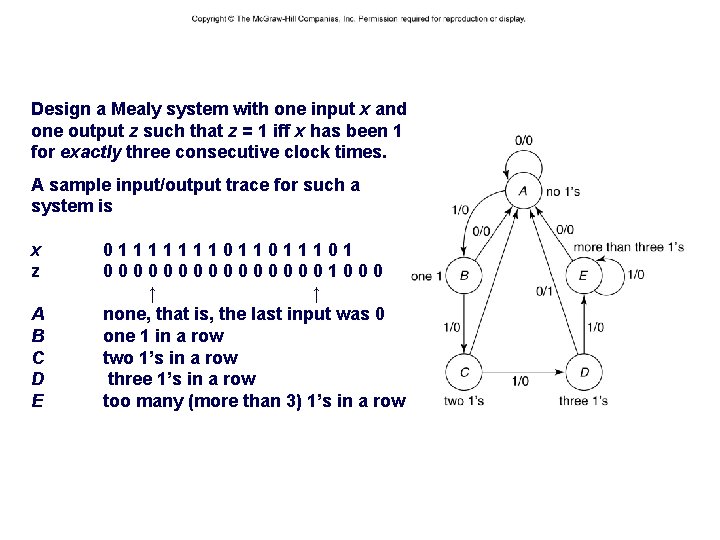
Design a Mealy system with one input x and one output z such that z = 1 iff x has been 1 for exactly three consecutive clock times. A sample input/output trace for such a system is x z A B C D E – 36 – 0111111101101 000000001000 ↑ ↑ none, that is, the last input was 0 one 1 in a row two 1’s in a row three 1’s in a row too many (more than 3) 1’s in a row CSCE 211 H Fall 2014

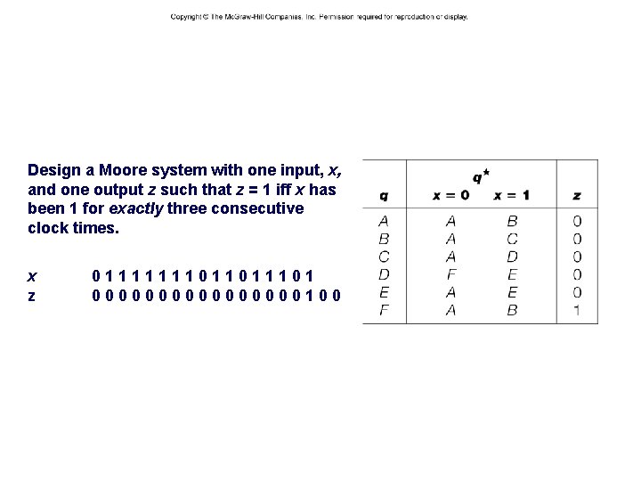
Design a Moore system with one input, x, and one output z such that z = 1 iff x has been 1 for exactly three consecutive clock times. x z – 37 – 0111111101101 00000000100 CSCE 211 H Fall 2014

CE 8. Design a Moore system whose output is 1 iff three consecutive 0 inputs occurred more recently than three consecutive 1 inputs. A sample input/output trace for such a system is – 38 – x 1110010000111101 z ? ? ? 0000000111100000 CSCE 211 H Fall 2014

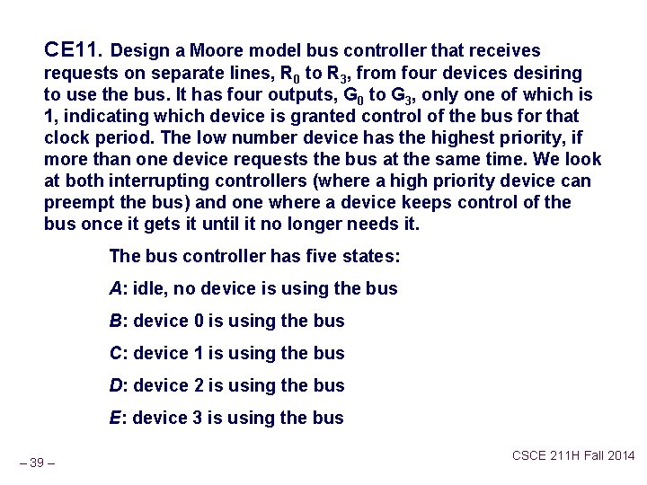
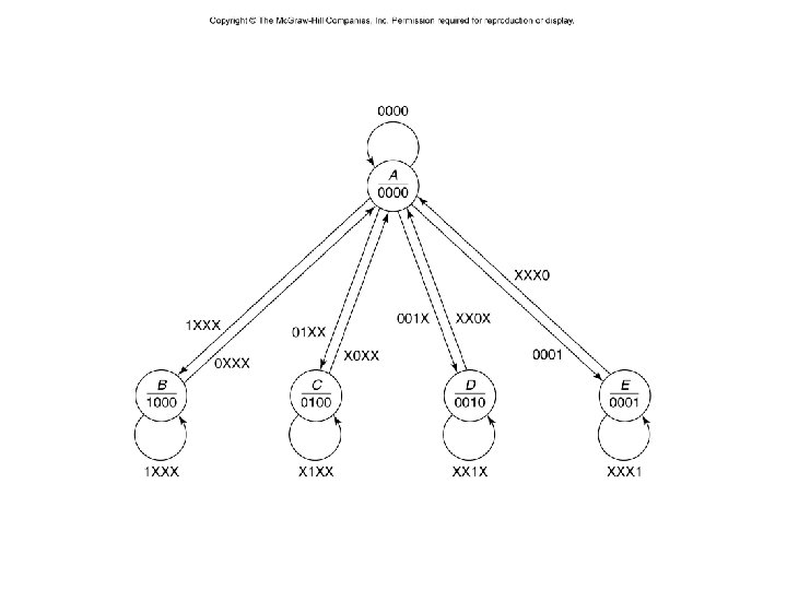
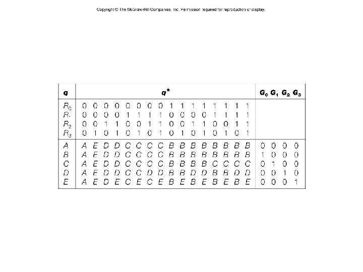
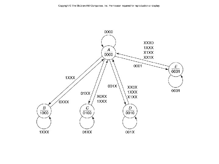
CE 11. Design a Moore model bus controller that receives requests on separate lines, R 0 to R 3, from four devices desiring to use the bus. It has four outputs, G 0 to G 3, only one of which is 1, indicating which device is granted control of the bus for that clock period. The low number device has the highest priority, if more than one device requests the bus at the same time. We look at both interrupting controllers (where a high priority device can preempt the bus) and one where a device keeps control of the bus once it gets it until it no longer needs it. The bus controller has five states: A: idle, no device is using the bus B: device 0 is using the bus C: device 1 is using the bus D: device 2 is using the bus E: device 3 is using the bus – 39 – CSCE 211 H Fall 2014

– 40 – CSCE 211 H Fall 2014

– 41 – CSCE 211 H Fall 2014

– 42 – CSCE 211 H Fall 2014

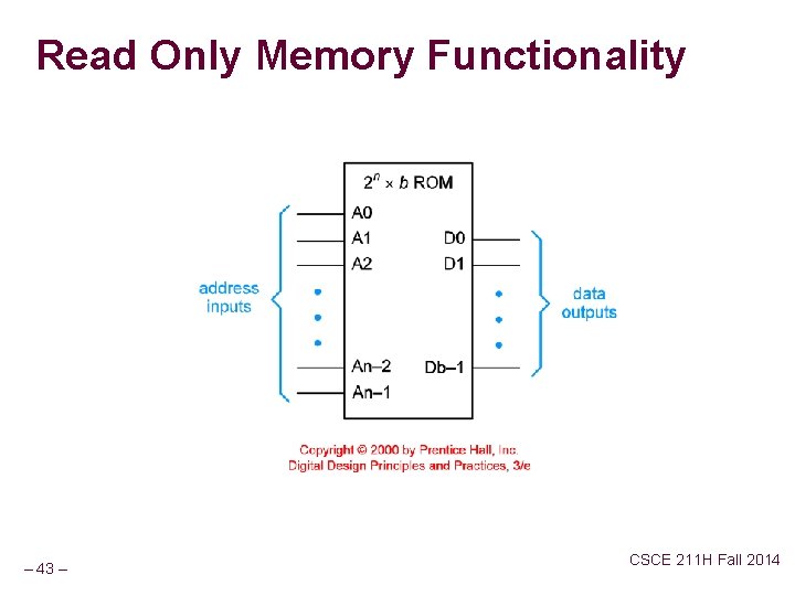
Read Only Memory Functionality – 43 – CSCE 211 H Fall 2014

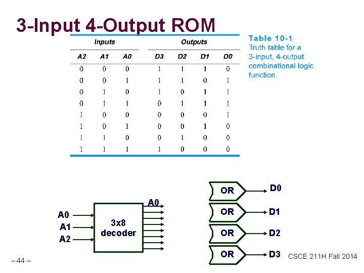
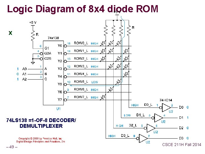
3 -Input 4 -Output ROM A 0 A 1 A 2 – 44 – 3 x 8 decoder OR D 0 OR D 1 OR D 2 OR D 3 CSCE 211 H Fall 2014

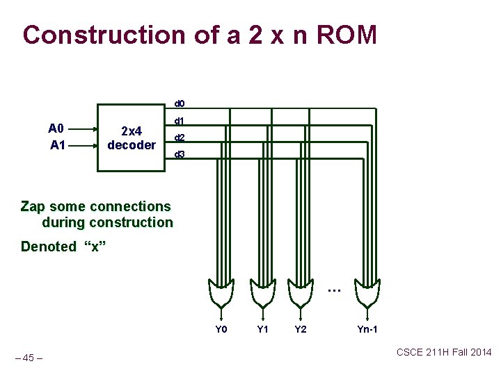
Construction of a 2 x n ROM d 0 A 1 2 x 4 decoder d 1 d 2 d 3 Zap some connections during construction Denoted “x” … Y 0 – 45 – Y 1 Y 2 Yn-1 CSCE 211 H Fall 2014

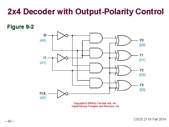
2 x 4 Decoder with Output-Polarity Control Figure 9 -2 – 46 – CSCE 211 H Fall 2014

Implementing Arbitrary Boolean functions with ROMs – 47 – CSCE 211 H Fall 2014

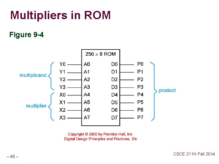
Multipliers in ROM Figure 9 -4 – 48 – CSCE 211 H Fall 2014

Logic Diagram of 8 x 4 diode ROM x 74 LS 138 =1 -OF-8 DECODER/ DEMULTIPLEXER – 49 – CSCE 211 H Fall 2014

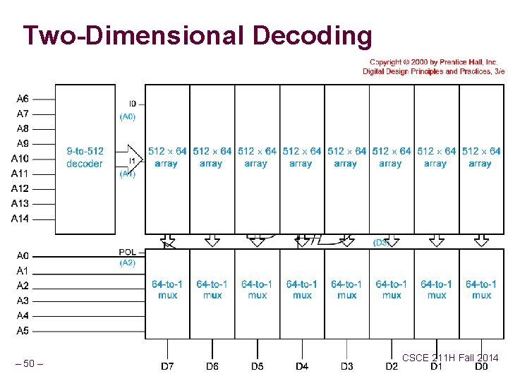
Two-Dimensional Decoding – 50 – CSCE 211 H Fall 2014

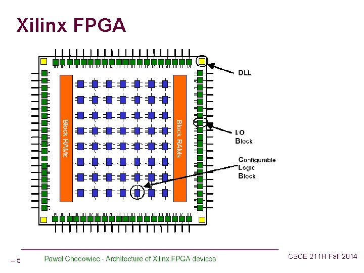
Field Programmable Gate Arrays Xilinx Spartan-3 FPGA family. n Download circuits onto the chip n FPGA l Field l Programmable l Gate array Spartan-3 FPGAs with 1 million system gates for under $12. 00 – 51 – CSCE 211 H Fall 2014

Xilinx FPGA – 52 – CSCE 211 H Fall 2014

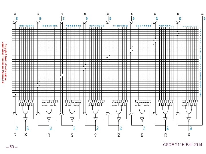
– 53 – CSCE 211 H Fall 2014