CSCE 211 Digital Design Lecture 10 Sequential Circuits



- Slides: 25

CSCE 211 Digital Design Lecture 10 Sequential Circuits The Basic Latch Topics n Sequential Circuits l SR Latch l Clocked SR l Master Slave n Master Slave VHDL Readings: 5. 4, 5. 9, 5. 10, 4. 4 October 19, 2015

Overview Last Time n Carry Look ahead n VHDL intro l n Test 1 New n n Sequential Circuits: Basic Nor Latch (really time before) Clocked SR flip flops Master Slave SR Test 1 HDL – 2– n Structural specifications CSCE 211 H Fall 2015

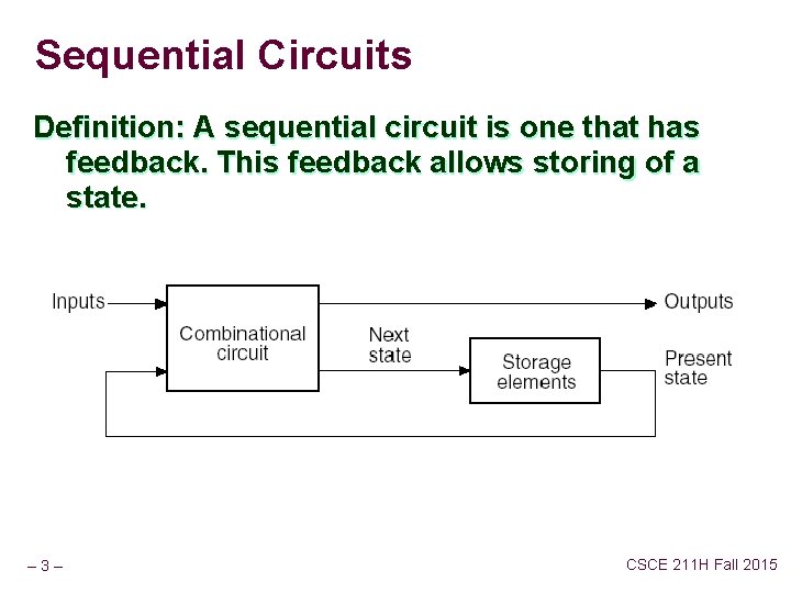
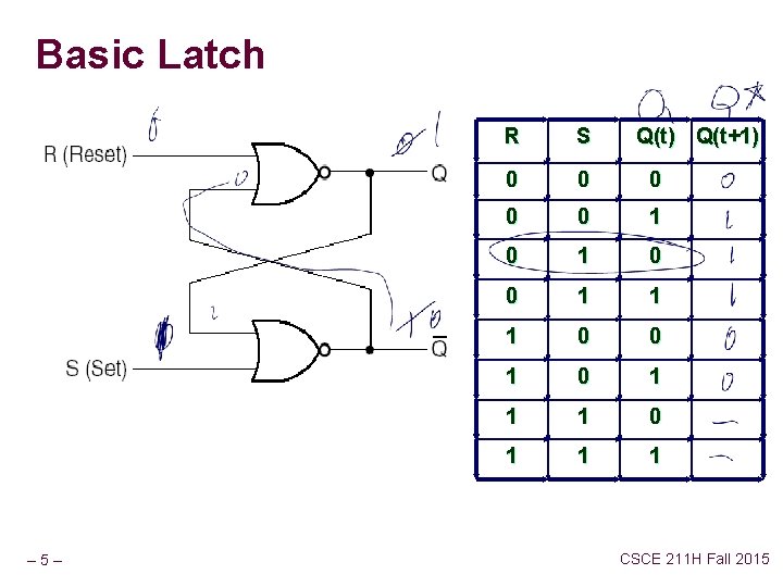
Sequential Circuits Definition: A sequential circuit is one that has feedback. This feedback allows storing of a state. – 3– CSCE 211 H Fall 2015

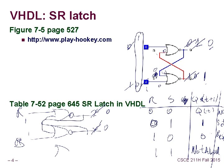
VHDL: SR latch Figure 7 -5 page 527 n http: //www. play-hookey. com Table 7 -52 page 645 SR Latch in VHDL – 4– CSCE 211 H Fall 2015

Basic Latch – 5– R S Q(t) Q(t+1) 0 0 0 1 1 1 0 0 1 1 1 CSCE 211 H Fall 2015

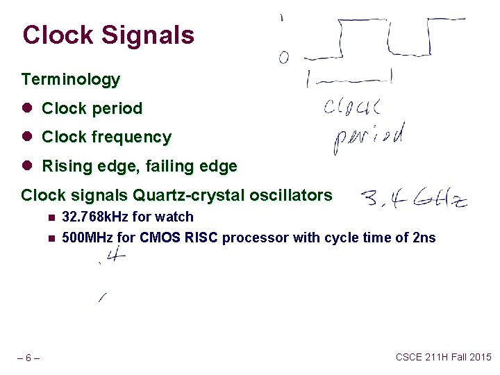
Clock Signals Terminology l Clock period l Clock frequency l Rising edge, failing edge Clock signals Quartz-crystal oscillators n n – 6– 32. 768 k. Hz for watch 500 MHz for CMOS RISC processor with cycle time of 2 ns CSCE 211 H Fall 2015

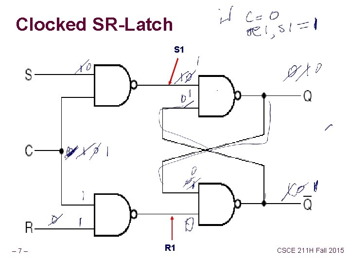
Clocked SR-Latch S 1 – 7– R 1 CSCE 211 H Fall 2015

Transition Table for Clocked SR flip-flop S – 8– R Q(t) Q* or Q(t+1) CSCE 211 H Fall 2015

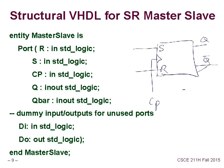
Structural VHDL for SR Master Slave entity Master. Slave is Port ( R : in std_logic; S : in std_logic; CP : in std_logic; Q : inout std_logic; Qbar : inout std_logic; -- dummy input/outputs for unused ports Di: in std_logic; Do: out std_logic); end Master. Slave; – 9– CSCE 211 H Fall 2015

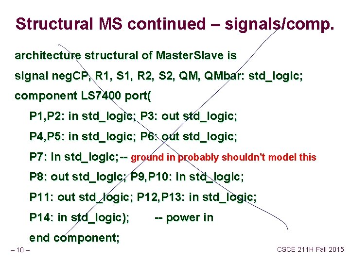
Structural MS continued – signals/comp. architecture structural of Master. Slave is signal neg. CP, R 1, S 1, R 2, S 2, QMbar: std_logic; component LS 7400 port( P 1, P 2: in std_logic; P 3: out std_logic; P 4, P 5: in std_logic; P 6: out std_logic; P 7: in std_logic; -- ground in probably shouldn’t model this P 8: out std_logic; P 9, P 10: in std_logic; P 11: out std_logic; P 12, P 13: in std_logic; P 14: in std_logic); -- power in end component; – 10 – CSCE 211 H Fall 2015

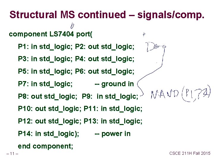
Structural MS continued – signals/component LS 7404 port( P 1: in std_logic; P 2: out std_logic; P 3: in std_logic; P 4: out std_logic; P 5: in std_logic; P 6: out std_logic; P 7: in std_logic; -- ground in P 8: out std_logic; P 9: in std_logic; P 10: out std_logic; P 11: in std_logic; P 12: out std_logic; P 13: in std_logic; P 14: in std_logic); -- power in end component; – 11 – CSCE 211 H Fall 2015

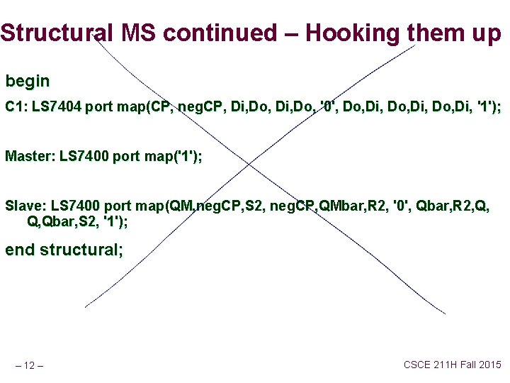
Structural MS continued – Hooking them up begin C 1: LS 7404 port map(CP, neg. CP, Di, Do, '0', Do, Di, '1'); Master: LS 7400 port map('1'); Slave: LS 7400 port map(QM, neg. CP, S 2, neg. CP, QMbar, R 2, '0', Qbar, R 2, Q, Q, Qbar, S 2, '1'); end structural; – 12 – CSCE 211 H Fall 2015

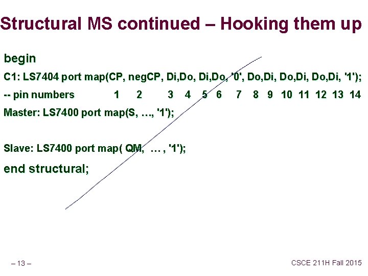
Structural MS continued – Hooking them up begin C 1: LS 7404 port map(CP, neg. CP, Di, Do, '0', Do, Di, '1'); -- pin numbers 1 2 3 4 5 6 7 8 9 10 11 12 13 14 Master: LS 7400 port map(S, …, '1'); Slave: LS 7400 port map( QM, … , '1'); end structural; – 13 – CSCE 211 H Fall 2015

Synthesize Notes Fill out the behavioral VHDL for the LS 7400 and LS 7404 Fill in the structural VHDL for the Master. Slave n n i. e. , connect the wires with signals Note we name the wires(signals) so that we can connect Change the inout to out on Q and Qbar and resynthsize. What is the result? – 14 – CSCE 211 H Fall 2015

Simulate the circuit What’s you plan? For stepping through all combinations you would like to see? Which input collection should you avoid? What happens if you simulate this input? – 15 – CSCE 211 H Fall 2015

S-R Flip Flop – 16 – CSCE 211 H Fall 2015

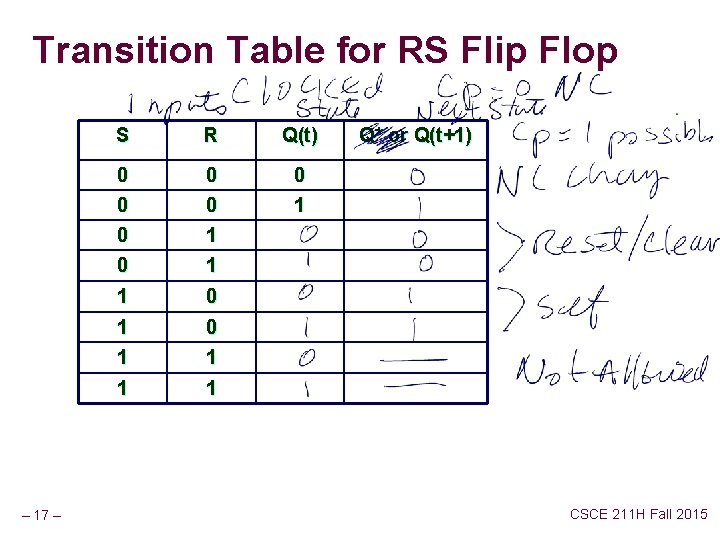
Transition Table for RS Flip Flop – 17 – S R Q(t) 0 0 0 1 0 1 1 1 Q* or Q(t+1) CSCE 211 H Fall 2015

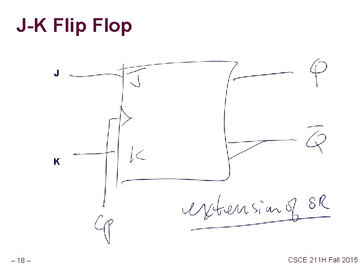
J-K Flip Flop J K – 18 – CSCE 211 H Fall 2015

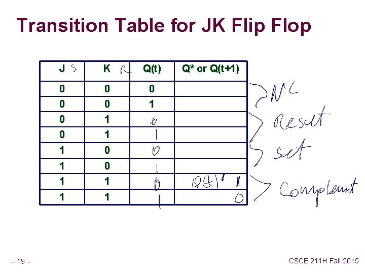
Transition Table for JK Flip Flop – 19 – J K Q(t) 0 0 0 1 0 1 1 1 Q* or Q(t+1) CSCE 211 H Fall 2015

– 20 – CSCE 211 H Fall 2015

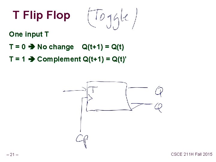
T Flip Flop One input T T = 0 No change Q(t+1) = Q(t) T = 1 Complement Q(t+1) = Q(t)’ – 21 – CSCE 211 H Fall 2015

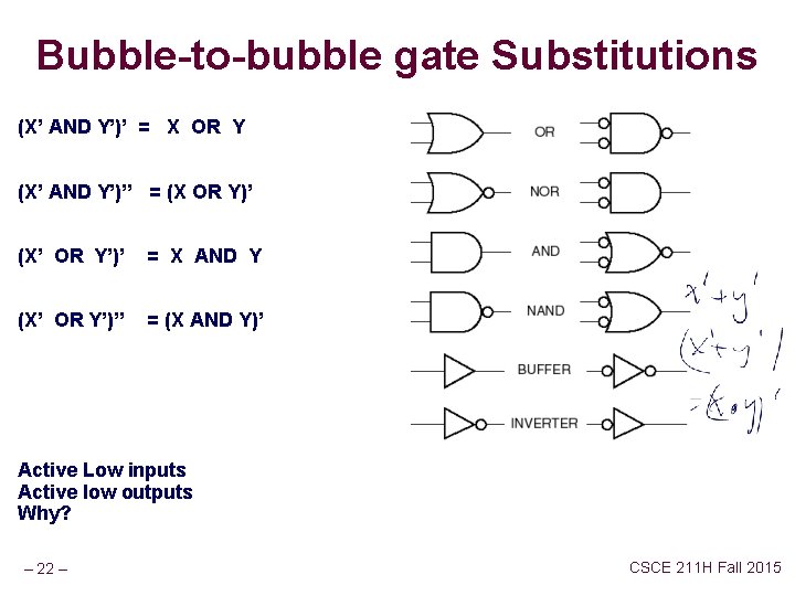
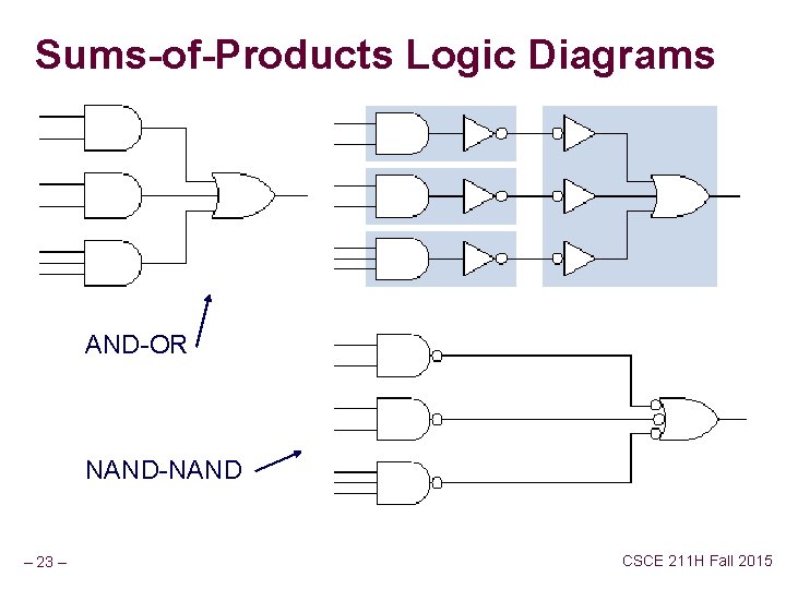
Bubble-to-bubble gate Substitutions (X’ AND Y’)’ = X OR Y (X’ AND Y’)’’ = (X OR Y)’ (X’ OR Y’)’ = X AND Y (X’ OR Y’)’’ = (X AND Y)’ Active Low inputs Active low outputs Why? – 22 – CSCE 211 H Fall 2015

Sums-of-Products Logic Diagrams AND-OR NAND-NAND – 23 – CSCE 211 H Fall 2015

– 24 – CSCE 211 H Fall 2015

– 25 – CSCE 211 H Fall 2015